

Page 1
Multiple RS-232 Drivers and Receivers
Features
·
Single-chip with easy interface between UART and
serial port connector
·
Three drivers and five receivers meet or exceed the
requirements of EIA/TIA-232-D
·
Designed to support data rates up to 120 Kbit/s
General Description
The HT6571 is a CMOS device containing three RS-232
line drivers, and five RS-232 line receivers that are used
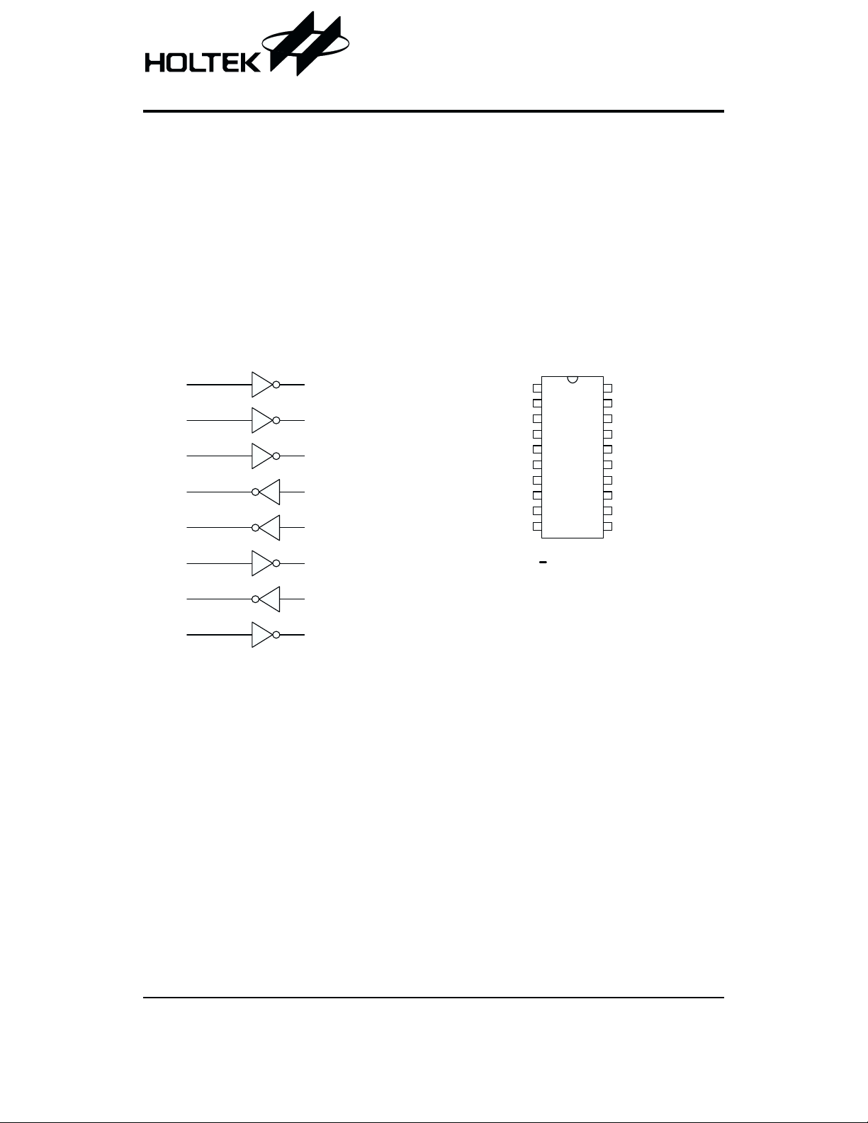
Block Diagram Pin Assignment
·
Driver current-limited output: 25mA typ.
·
Flexible supply voltage range
·
ESD protection exceeds 5kV
·
20-pin SOP package
to interface data terminal equipment (DTE) with data cir
cuit-terminating equipment (DCE).
HT6571
-
R A 1
R A 2
R A 3
D Y 1
D Y 2
R Y 1
R Y 2
R Y 3
D A 1
D A 2
V D D
R A 1
R A 2
R A 3
D Y 1
D Y 2
R A 4
D Y 3
R A 5
V S S
1
2
3
4
5
6
7
8
9
1 0
2 0
V C C
1 9
R Y 1
1 8
R Y 2
1 7
R Y 3
1 6
D A 1
1 5
D A 2
1 4
R Y 4
1 3
D A 3
1 2
R Y 5
1 1
G N D
H T 6 5 7 1
R A 4
D Y 3
R A 5
R Y 4
D A 3
R Y 5
2 0 S O P - A
Absolute Maximum Ratings
Supply Voltage (VSS VDD).......................... -15V~15V
Input Voltage Driver .......................................... 0V~7V
Output Voltage Driver .................................. -15V~15V Receiver ............................................................ 0V~7V
Supply Voltage (GND VCC)....................... -0.3V~5.5V
Receiver ...................................................... -15V~15V
Note: These are stress ratings only. Stresses exceeding the range specified under ²Absolute Maximum Ratings² may
cause substantial damage to the device. Functional operation of this device at other conditions beyond those
listed in the specification is not implied and prolonged exposure to extreme conditions may affect device reliabil
ity.
Rev. 1.20 1 August 20, 2002
-
Page 2
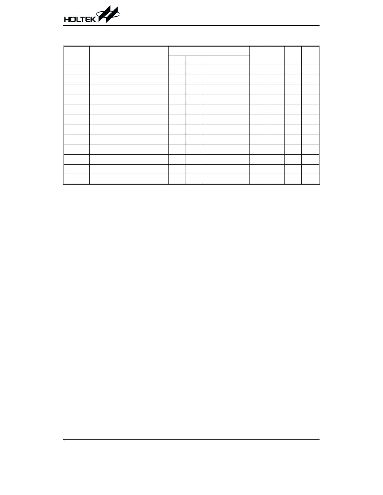
Electrical Characteristics
Symbol Paremeter
V
DD
V
SS
V
CC
V
IH1
V
IL1
V
IH2
V
IL2
I
OH1
I
OL1
I
OS(H)
I
OS(L)
S
R1
Operation Voltage
Operation Voltage
Operation Voltage
Driver Input High 12V 5V 2
Driver Input Low 12V 5V
Receiver Input High 12V 5V 3
Receiver Input Low 12V 5V
Receiver Output Source Current 12V 5V
Receiver Output Sink Current 12V 5V VO=0.4V +1 +2 +3 mA
High-level Driver Short Current 12V 5V
Low-level Driver Short Current 12V 5V VO=0V 15 25 35 mA
Slew Rate 12V 5V
Test Conditions
V
DDVCC
Conditions
¾¾ ¾
Min. Typ. Max. Unit
7.5 9 15 V
¾¾ ¾ -7.5 -9 -15
¾¾ ¾
4.5 5 5.5 V
¾¾
¾¾
¾¾
¾¾
=2.4V
V
O
=0V
V
O
=7kW,C1=330pF ¾¾
R
L
-1 -2 -3
-15 -25 -35
HT6571
V
V
0.8 V
V
0V
mA
mA
30
V/ms
Rev. 1.20 2 August 20, 2002
Page 3
Application Circuits
HT6571
Rev. 1.20 3 August 20, 2002
Page 4

HT6571
,
,
Rev. 1.20 4 August 20, 2002
Page 5

Package Information
20-pin SOP (300mil) outline dimensions
HT6571
2 0
A
1
C
C '
D
E F
Symbol
A 394
B 290
C14
C¢
D92
E
F4
G32
H4
1 1
B
1 0
G
H
=
Dimensions in mil
Min. Nom. Max.
¾
¾
¾
490
¾
¾
¾
50
¾¾
¾
¾
a 0°¾10°
419
300
20
510
104
¾
38
12
Rev. 1.20 5 August 20, 2002
Page 6

Product Tape and Reel Specifications
Reel dimensions
HT6571
6
)
*
6
,
SOP 20W
Symbol Description Dimensions in mm
A Reel Outer Diameter
B Reel Inner Diameter
C Spindle Hole Diameter
D Key Slit Width
T1 Space Between Flange
T2 Reel Thickness
330±1.0
62±1.5
13.0+0.5
2.0±0.5
24.8+0.3
30.2±0.2
+
-0.2
-0.2
Rev. 1.20 6 August 20, 2002
Page 7

Carrier tape dimensions
HT6571
D
E
F
PD 1
P 1P 0
W
A 0
B 0
C
SOP 20W
Symbol Description Dimensions in mm
W Carrier Tape Width
P Cavity Pitch
E Perforation Position
F Cavity to Perforation (Width Direction)
24.0+0.3
-0.1
12.0±0.1
1.75±0.1
11.5±0.1
D Perforation Diameter 1.5+0.1
D1 Cavity Hole Diameter 1.5+0.25
P0 Perforation Pitch
P1 Cavity to Perforation (Length Direction)
A0 Cavity Length
B0 Cavity Width
K0 Cavity Depth
t Carrier Tape Thickness
4.0±0.1
2.0±0.1
10.8±0.1
13.3±0.1
3.2±0.1
0.3±0.05
C Cover Tape Width 21.3
t
K 0
Rev. 1.20 7 August 20, 2002
Page 8

HT6571
Holtek Semiconductor Inc. (Headquarters)
No.3, Creation Rd. II, Science-based Industrial Park, Hsinchu, Taiwan
Tel: 886-3-563-1999
Fax: 886-3-563-1189
http://www.holtek.com.tw
Holtek Semiconductor Inc. (Sales Office)
11F, No.576, Sec.7 Chung Hsiao E. Rd., Taipei, Taiwan
Tel: 886-2-2782-9635
Fax: 886-2-2782-9636
Fax: 886-2-2782-7128 (International sales hotline)
Holtek Semiconductor (Shanghai) Inc.
7th Floor, Building 2, No.889, Yi Shan Rd., Shanghai, China
Tel: 021-6485-5560
Fax: 021-6485-0313
http://www.holtek.com.cn
Holtek Semiconductor (Hong Kong) Ltd.
RM.711, Tower 2, Cheung Sha Wan Plaza, 833 Cheung Sha Wan Rd., Kowloon, Hong Kong
Tel: 852-2-745-8288
Fax: 852-2-742-8657
Holmate Semiconductor, Inc.
48531 Warm Springs Boulevard, Suite 413, Fremont, CA 94539
Tel: 510-252-9880
Fax: 510-252-9885
http://www.holmate.com
Copyright Ó 2002 by HOLTEK SEMICONDUCTOR INC.
The information appearing in this Data Sheet is believed to be accurate at the time of publication. However, Holtek as
sumes no responsibility arising from the use of the specifications described. The applications mentioned herein are used
solely for the purpose of illustration and Holtek makes no warranty or representation that such applications will be suitable
without further modification, nor recommends the use of its products for application that may present a risk to human life
due to malfunction or otherwise. Holtek reserves the right to alter its products without prior notification. For the most
up-to-date information, please visit our web site at http://www.holtek.com.tw.
-
Rev. 1.20 8 August 20, 2002
 Loading...