

Page 1
Features
•
Operating voltage: 2.2V ~3.6V
•
Ten bidirectional I/O lines
•
Six schmitt trigger input lines
•
One carrier output (1/2 or 1/3 duty)
•
On-chip crystal and RC oscillator
•
Watchdog timer
•
1K×14 program ROM
•
32×8 data RAM
•
Low voltage reset function
General Description
The HT48CA0 is an 8-bit high performance
RISC-like micro controller specifically d es igned
for multiple I/O prod uct applications. The device is particularly suita ble for use in prod ucts
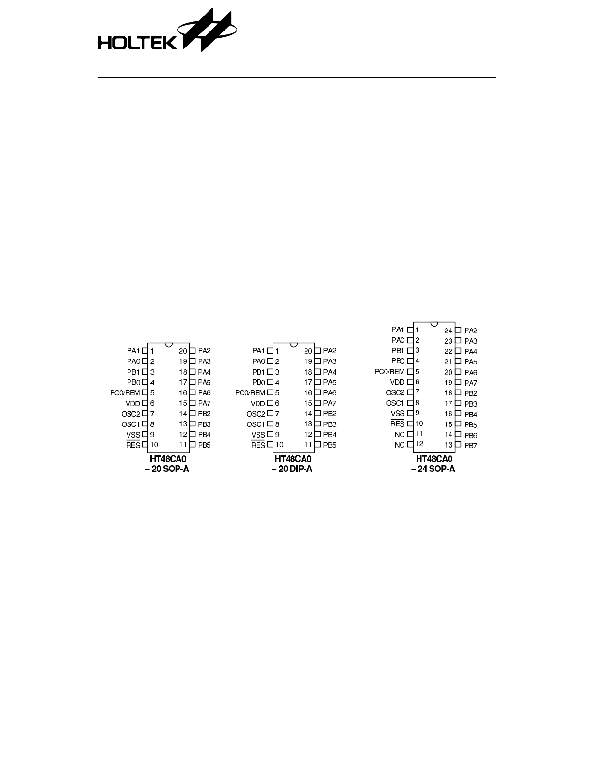
Pin Assignment
HT48CA0
8-bit Microcontroller
•
Halt function and wake-up feature reduce
power consumption
•
62 powerful instructions
•
Up to 1µs instruction cycle with 4MHz
system clock
•
All instructions in 1 or 2 machine cycles
•
14-bit table read instructions
•
One-level subroutine nesting
•
Bit manipulation instructions
such as remote controllers, fan/light controllers, washing machi ne controllers, sca les, toys
and various subsystem controllers. A halt feature is included to reduce power consumption.
1 23rd July ’98
Page 2
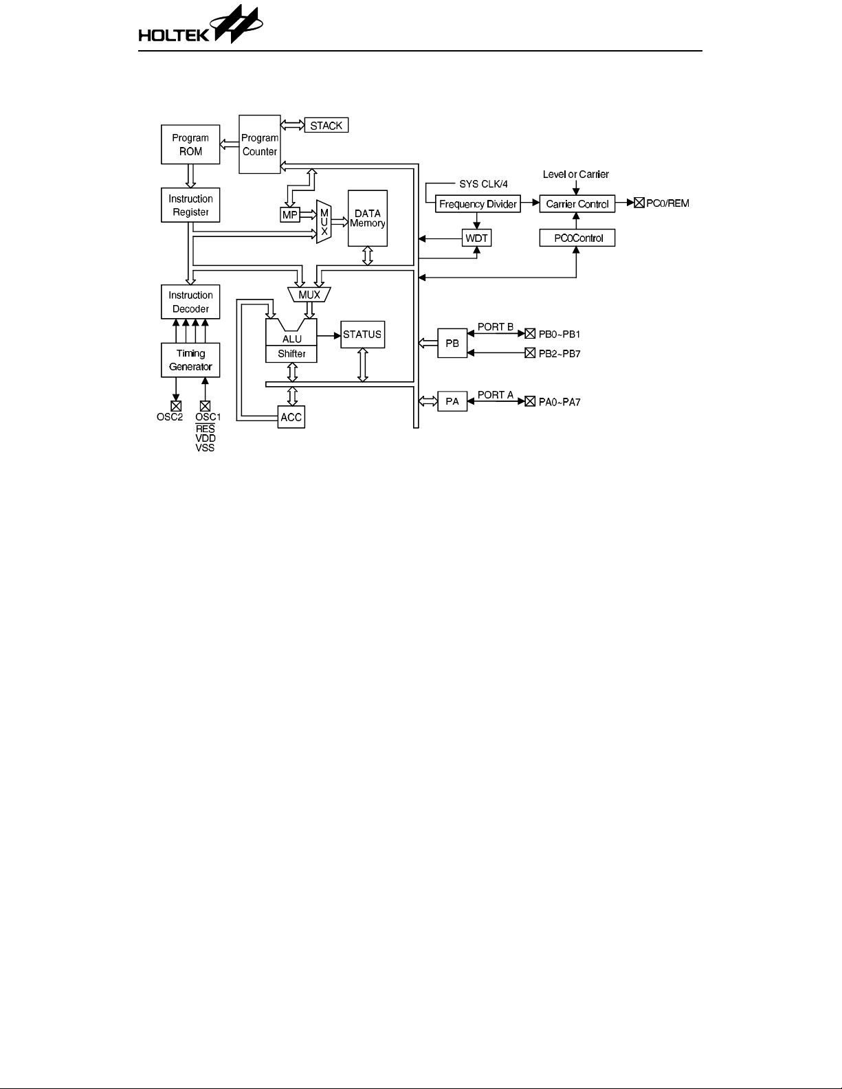
Block Diagram
HT48CA0
2 23rd July ’98
Page 3

Pad Description
HT48CA0
Pad No. Pad Name I/O
1, 22 PB0, PB1 I/O
2 PC0/REM O
3 VDD — — Positive power supply
6 VSS — — Negative power supply, GND
7
13~8 PB2~PB7 I
21~14 PA0~PA7 I/O —
RES I — Schmitt trigger reset input. Active low.
OSC1
OSC2
Mask
Option
Wake-up
or None
Level or
Carrier
Wake-up
or None
IOCrystal or
RC
Function
2-bit bidirectional input/output lines with pull-high
resistors. Each bit can be determined as NMOS output
or schmitt trigger input by software instructions. Each
bit can also be configu red as wake-up i nput by mask
option.
Level or carrier output pin
PC0 can be set as C MO S outp ut pin o r carri er outp ut
pin by mask option.
6-bit schmitt trigger input lines with pull-high
resistors. Each bit can be configured as a wake-up
input by mask option .
Bidirectional 8-bit input/output port with pull-high
resistors. Each bit can be determined as NMOS output
or schmitt trigger input by software instructions.
OSC1, OSC2 are connected to an RC network or a
crystal (determined by mask option) for the internal
system clock. In the case of RC operation, OSC2 is the
output terminal for 1/4 system clock (NMOS open
drain output).
3 23rd July ’98
Page 4
Pad Assignment
* The IC substrate should be connected to VSS in the PCB layout artwork.
* The TMR pad must be bonded to VDD or VSS if the TMR pad is not used.
HT48CA0
Absolu te Maxim um Ratings *
Supply Voltage.................................–0.3V to 4V Storage Temperature.................–50°C to 125°C
Input Voltage................. V
*Note: These are stress ra tings on ly. Stresses exceeding the range specified under “Ab solute Maxi -
mum Ratings” ma y cause substantial damage to the device. Functional operation of this
device at other conditions beyond those listed in the specification is not implied and prolonged
exposure to extreme condition s may affect device reliability.
–0.3V to VDD+0.3V Operating Temperature............... –25°C to 70°C
SS
4 23rd July ’98
Page 5
HT48CA0
D.C. Characteristics Ta=25°C
Symbol Parameter
V
I
DD
I
STB
V
V
V
V
I
OL
I
OH
R
R
V
Operating Voltage — — 2.2 — 3.6 V
DD
Operating Current 3V
Standby Current 3V
Input Low Voltage for I/O Ports 3V — 0 — 1.05 V
IL1
Input High Voltage for I/O Ports 3V — 1.95 — 3 V
IH1
Input Low Voltage (RES) 3V — — 1.5 — V
IL2
Input High Voltage (RES) 3V — — 2.4 — V
IH2
I/O Ports Sink Current 3V VOL=0.3V 1.5 2.5 — mA
I/O Ports Source Current 3V VOH=2.7V –1 –1.5 — mA
Pull-high Resistance of PA
PH1
Port, PB0~PB1 and
Pull-high Resistance of PB2~PB7 3V — — 60 — kΩ
PH2
Low Voltage Reset 3V — 1.8 2.0 2.2 V
LVR
RES
Test Conditions
V
DD
Conditions
No load,
f
=4MHz
SYS
No load,
system HALT
Min. Typ. Max. Unit
— 0.7 1.5 mA
——1µA
3V — — 60 — k
Ω
A.C. Characteristics Ta=25°C
Symbol Parameter
f
SYS
t
RES
t
SST
Note: t
System Clock 3V — 400 — 4000 kHz
External Reset Low Pulse Width — — 1 — — µs
System Start-up timer
Period
=1/f
SYS
SYS
Test Conditions
V
DD
—
Conditions
Power-up or
wake-up from halt
5 23rd July ’98
Min. Typ. Max. Unit
—1024—t
SYS
Page 6
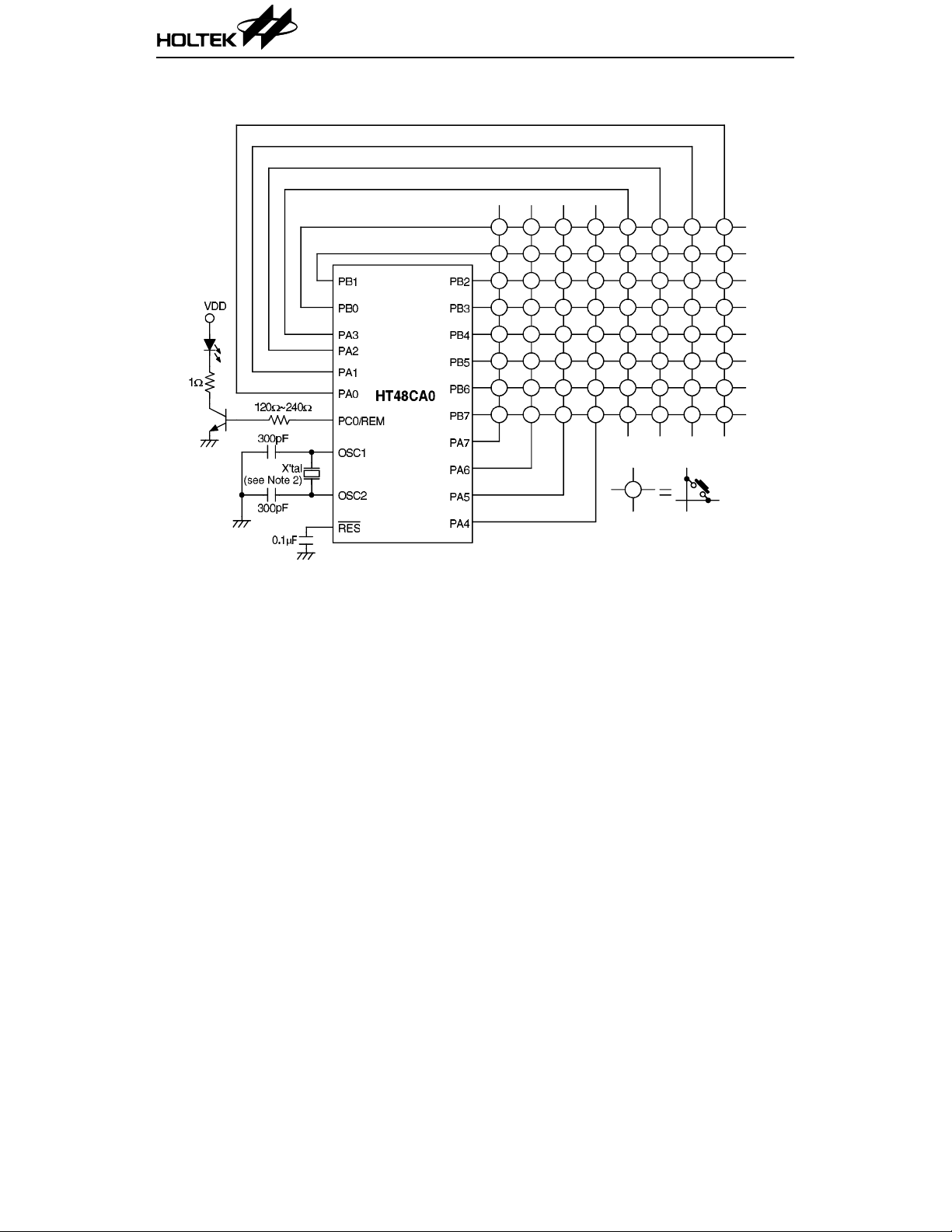
Application Circuit
HT48CA0
Notes: It is recommended tha t a 0.1µF decoupling capacitor is placed between VSS and VDD.
If the crystal has a value above 1MHz the capacitors are not required.
6 23rd July ’98
Page 7
System Architect ure
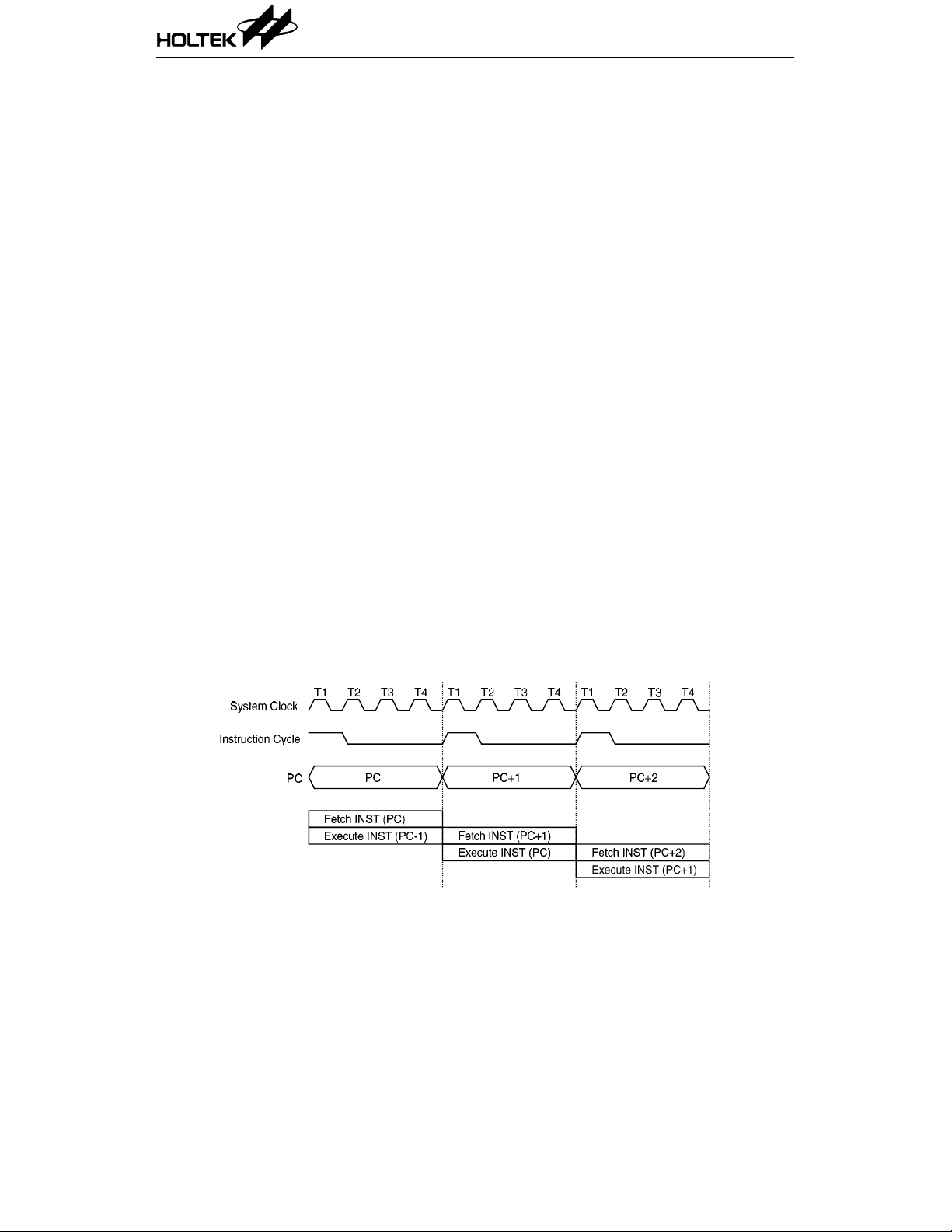
Execution flow
The HT48CA0 system clock can be derived from
a crystal/ceramic res onator oscillator. It is internally divided into four non-overlapping
clocks. One instruction cycle consists of four
system clock cycles.
Instruction fetching and execution are pipelined in such a wa y that a fetch takes one instruction cycle while decoding and execution
takes the next instructi on cycle. However, the
pipelining scheme causes each instruction to
effectively execute within one cycle. If an instruction changes the program cou nte r, two cycles are required to comp lete the instruction.
Program counter – PC
The 10-bit program co unter (PC) controls the
sequence in which the instructions stored in
program ROM are executed and its contents
specify a maximum of 10 24 addresses.
After accessing a program memory word to
fetch an instruction code, the contents of the
program counter are incremented by one. The
program counter then points to the memory
word containing the next instruction code.
When executing a jump instruction, conditional
skip execution, loading PCL register, subroutine call, initial reset or return from subroutine,
the PC manipulates the program transfer by
loading the addr ess corresponding to each instruction.
HT48CA0
The conditional skip is activated by instruction.
Once the condition is met, the next instruction,
fetched during the current instruction execution, is discarded and a dummy cycle replaces it
to get the proper instruction. Otherwise proceed with the next instruction.
The lower byte of the program counter (PCL) is
a readable and writeable re gister (06H). Moving data into the PCL performs a short jump.
The destination will be within 256 locations.
When a control tran sfer takes place, an additional dummy cycle is required.
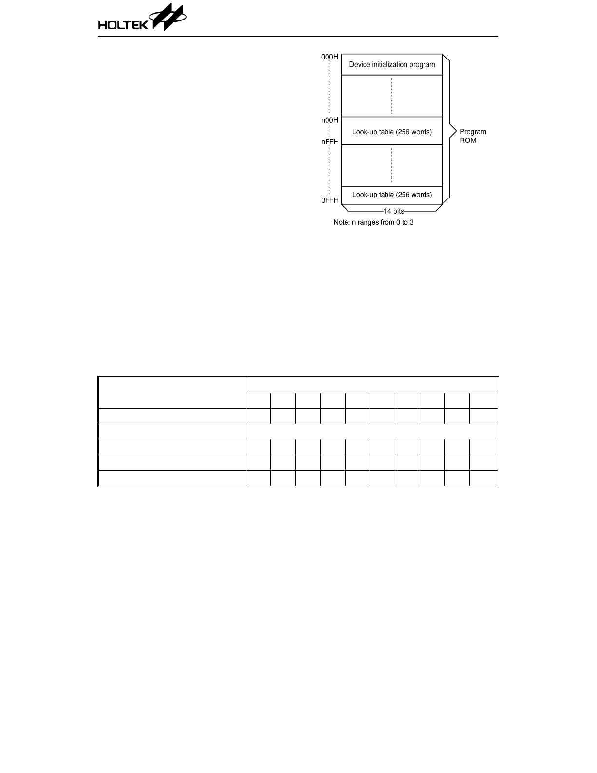
Program memory – ROM
The program memory is used to store the program instructions which are to be executed. It
also contains data and ta ble and is organized
into 1024
counter and table pointer.
Certain locations in the progra m memory are
reserved for special usage:
•
Location 000H
This area is reserved for the initialization
program. After chip reset, the program always
begins execution at location 000H.
•
Table location
Any location in the ROM space can be used as
look-up tables. The instructions TABRDC [m]
(the current page, 1 page=256 words) and
TABRDL [m] (the last page) transfer the contents of the lower-order byte to the specified
×14 bits, addressed by the program
Execution flow
7 23rd July ’98
Page 8
data memory, and the higher-order byte to
TBLH (08H). Only the destination of the
lower-order byte in the table is well-defin ed,
the other bits of the table word are transferred
to the lower portion of TBLH, the remaining 2
bits are read as “0”. The Table Higher-order
byte register (TBLH) is read only. The tab le
pointer (TBLP) is a read/write regi ster (07H),
where P indicates the table location. Before
accessing the table, the location must be
placed in TBLP. The TBLH is read only and
cannot be restore d. All table related instructions need 2 cycles to com ple te the o pera tio n.
These areas may function as normal program
memory depending upon the requirements.
Stack register – STACK
This is a special part of the memory used to save
the contents of the progra m counter (PC) only.
The stack is organized into one level and is
neither part of the data nor part of the program
space, and is neither readable nor writeable.
The activated level is indexed by the stack
pointer (SP) and is neith er readable nor writeable. At a subroutine call the contents of the
program counter are pushed onto th e stack. At
the end of a subroutine signaled by a return
instruction (RET), the program counter is restored to its previous value from the stack. After
a chip reset, the SP will point to the top of the stack.
HT48CA0
Program memory
If the stack is full and a “CALL” is subsequently
executed, stack overflow occurs and the first
entry will be lost (o nly the most recent retu rn
address is stored).
Data memory – RAM
The data memory is designed wi th 42×8 bits.
The data memory is divided into two functional
groups: special function re gisters and general
purpose data memory (32
read/write, but some are read only.
×8). Most of them are
Mode
Program Counter
*9 *8 *7 *6 *5 *4 *3 *2 *1 *0
Initial reset 0000000000
Skip
Loading PCL *9 *8@7@6@5@4@3@2@1 @0
Jump, call branch #9 #8 #7 #6 #5 #4 #3 #2 #1 #0
Return from subroutine S9 S8 S7 S6 S5 S4 S3 S2 S1 S0
Program counter
Notes: *9~*0: Program counter bits
#9~#0: Instruction code bits
8 23rd July ’98
PC+2
S9~S0: Stack register bits
@7~@0: PCL bits
Page 9
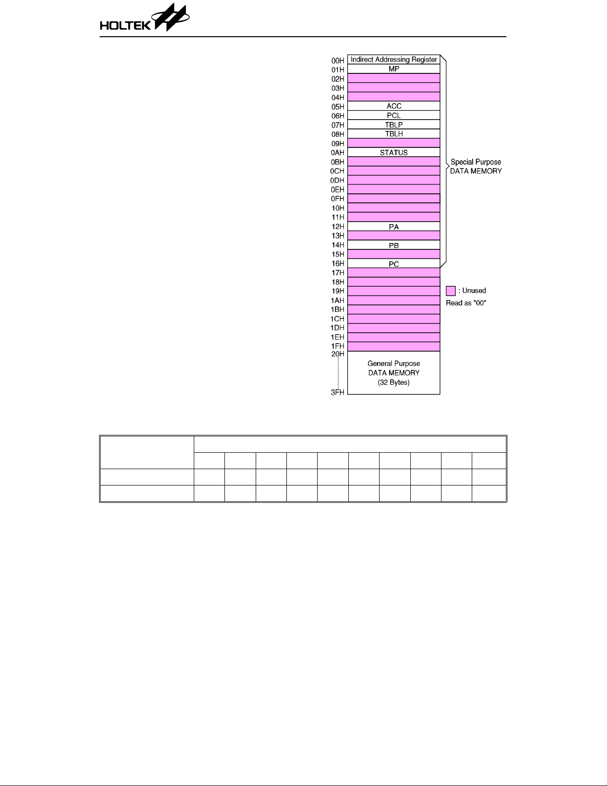
The special function registers include the indirect
addressing register (00H), the memory pointer
register (MP;01H), the accumulator (ACC;05H)
the program counter lower-order byte register
(PCL;06H), the table pointer (TBLP;07H), the table higher-order byte register (TBLH;08H), the
status register (STATUS;0AH) and the I/O registers (PA;12H, PB;14H, PC;16H). The remaining
space before the 20H is reserved for future expanded usage and reading these locations will
return the result 00H. The general purpose data
memory, addressed from 20H to 3FH, is used for
data and control information under instruction
command.
All data memory areas can hand le arithmetic,
logic, increment, decrement and ro tate operations directly. Except for some ded icated bits,
each bit in the data memory can be set and reset
by the SET [m].i and CLR [m].i instructions,
respectively. They are also indirectly accessible
through memory pointer register (MP;01H).
Indirect addressing register
Location 00H is an indirect addressing register
that is not physically implemented. Any
read/write operation of [00H] accesses data
memory pointed to by MP (01H). Reading location 00H itself indire ctly will return th e result
00H. Writing indirectly results in no operation.
The memory pointer register MP (01H) is a 6-bit
register. The bit 7~6 of MP is undefined and
reading will return the result “1” . Any writing
operation to MP will only transfer the lower 6-bit
data to MP.
HT48CA0
RAM mapping
Instruction(s)
Ta ble Loc ation
*9 *8 *7 *6 *5 *4 *3 *2 *1 *0
TABRDC [m] P9 P8 @7 @6 @5 @4 @3 @2 @1 @0
TABRDL [m] 1 1 @7 @6 @5 @4 @3 @2 @1 @0
Table location
Notes: *9~*0: Table location bits
@7~@0: Table pointer bits
9 23rd July ’98
P9~P8: Current program counter bits
Page 10

Accumulator
The accumulator clo sely relates to ALU opera tions. It is also mappe d to location 05H of the
data memory and is capable of carrying out
immediate data operations. Data movement between two data memory loca tions has to pass
through the accumulator.
Arithmetic and logic unit – ALU
This circuit performs 8-bit arithmetic and logic
operation. The ALU provides the following functions.
•
Arithmetic operations (ADD, ADC, SUB,
SBC, DAA)
•
Logic operations (AND, OR, XOR, CPL)
•
Rotation (RL, RR, RLC, RRC)
•
Increment and Decrement (INC, DEC)
•
Branch decision (SZ, SNZ, SIZ, SDZ ....)
The ALU not only saves the results of a data
operation but also changes the contents of the
status register.
Status register – STATUS
This 8-bit status register (0AH) contains the zero
flag (Z), carry flag (C), auxiliary carry flag (AC),
HT48CA0
overflow flag (OV), power down flag (PD) and
watchdog time -out flag (TO). It also recor ds the
status information and controls the operation
sequence.
With the exception of the TO and PD flags, bits
in the status register can be altered by instructions like most other register. Any data written
into the status register will not change the TO
or PD flags. I n a d diti on it sh ou ld be note d that
operations related to the status register may
give different results from th ose intende d. The
TO and PD flags can only be changed by the
W atchdog Timer overflow, chip power-up, clearing the Watchdog Timer and executing the
HALT instruction.
The Z, OV, AC and C flags generally reflect the
status of the latest operations.
In addition, on executing the subrouti ne call,
the status register will not be automatically
pushed onto the stack. If the contents of the
status are impo rtant and if the sub routine can
corrupt the status register, precautions must be
taken to save it properly.
Labels Bits Function
C is set if the operati on results in a carry during an addition op eration or if a
C0
borrow does not take place during a subtraction operation; otherwise C is
cleared. C is also affected by a rotate through carry instruction.
AC is set if the operation results in a carry ou t of the low nibbles in additio n or
AC 1
no borrow from the high nibble into the low nibble in subtraction; otherwise AC
is cleared.
Z2
OV 3
PD 4
TO 5
Z is set if the resul t of an arithmetic or logi c operation is zero; otherwise Z is
cleared.
OV is set if the operati on re sults in a carry in to the high est-order bi t but not a
carry out of the highest-order bit, or vice versa; otherwise OV is cleared.
PD is cleared when either a system power-up or executing the CLR WDT
instruction. PD is set by executing the HALT instruction.
TO is cleared by a system power-up or executing the CLR WDT or HALT
instruction. TO is set by a WDT time-out.
— 6 Undefined, read as “0”
— 7 Undefined, read as “0”
Status register
10 23rd July ’98
Page 11
Oscillator configuration
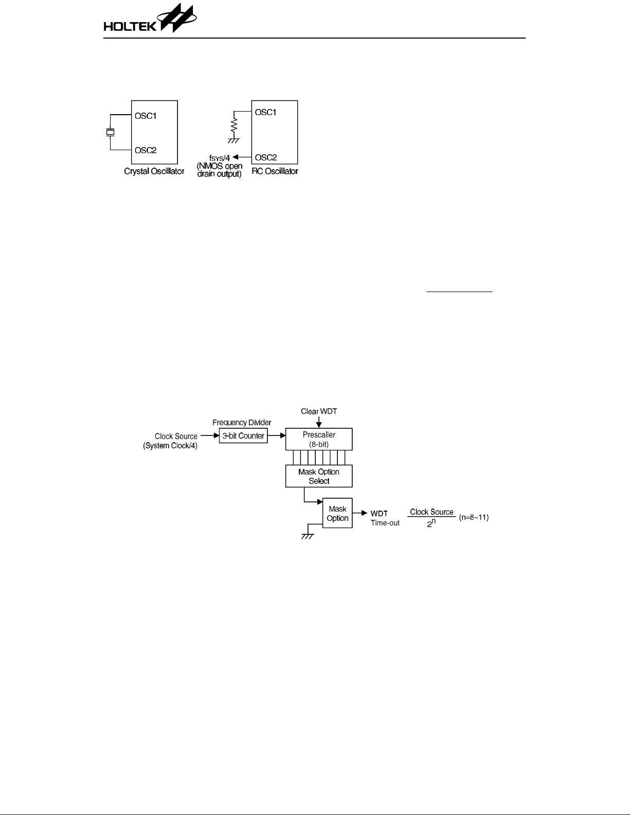
There are two oscillator circuits in the HT48CA0.
System oscillator
Both are designed for system clocks; the RC
oscillator and the Crystal oscillator, which are
determined by mask options. No matter what
oscillator typ e is selected, the si gnal provides
the system clock. The HALT mode stops the
system oscillator and igno res the external signal to conserve power.
If an RC oscillator is u sed, an e xtern al res istor
between OSC1 and VSS in needed and the resistance must range from 51k
Ω to 1MΩ. The
system clock, divided by 4, is available on
OSC2, which can be u se d to synch ron ize exte rnal logic. The RC oscillator provides the most
cost effective solution. However, the frequency
of the oscillation may vary with VDD, temperature and the chip itself due to process vari-
HT48CA0
ations. It is, therefore, not suitable for timing
sensitive operations where accurate os cillator
frequency is desired.
If the Crystal oscillator is used, a crystal across
OSC1 and OSC2 is need ed to provi de the feedback and phase shift for the oscillator. No other
external compone nts are needed. Instead of a
crystal, the resonator can also be connected
between OSC1 and OSC2 to get a frequency
reference, but two external capacitors in OSC1
and OSC2 are required.
Watchdog timer – WDT
The clock source of the WDT is implemented by
instruction clock (system clock divided by 4).
The clock source is processed by a frequency
divider and a prescaller to yield various time
out periods.
WDT time out period =
Where n= 8~11 selected by mask option.
This timer is designed to prevent a software
malfunction or sequence jumping to an unknown location with unpredictable results. The
Watchdog Timer can be disabled by mask option. If t he Watchdog Timer i s di sabl ed , al l th e
executions related to the WDT result in no op-
Clock Source
n
2
Watchdog timer
11 23rd July ’98
Page 12

HT48CA0
eration and the WDT will lose its protection
purpose. I n this situa tion the logic can only be
restarted by an external logic.
A WDT overflow under normal operation will initialize “chip reset” and set the status bit "TO". To
clear the contents of the WDT prescaler, three
methods are adopted; external reset (a low level to
RES), software instructions, or a HALT instruction. There are two types of software instructions.
One type is the single instruction "CLR WDT", the
other type comprises two instructions, "CLR
WDT1" and "CLR WDT2". Of these two types of
instructions, only one can be active depending on
the mask option — “CLR WDT times selection
option”. If the “CLR WDT” is selected (i.e..
CLRWDT times equal one), any execution of the
CLR WDT instruction will clear the WDT. In case
“CLR WDT1” and “CLR WDT2” are chosen (i.e..
CLRWDT times equal two), these two instructions must be executed to clear the WDT; otherwise, the WDT may reset the chip due to a
time-out.
Power down operation – HA L T
The HALT mode is initialized by the HALT
instruction and results in the following...
•
The system o scillator turns off and the WDT
stops.
•
The contents of the on-chip RAM and registers remain unchanged.
•
WDT prescaler are cleared.
•
All I/O ports maintain their original status.
•
The PD flag is set and the TO flag is cleared.
The system can quit the HALT mode by means
of an external reset or an external falling edge
signal on port B. An external reset causes a
device initialization. Examining the TO and PD
flags, the reason for chip reset can be determined. The PD flag is cleared when the system
powers up or execute the CLR WDT instruction
and is set when the HALT instruction is executed. The TO flag is set if the WDT time-out
occurs, and causes a wake-up that only resets
the PC (Program Counter) and SP, the others
keep their original status.
The port B wake-up can be considered as a
continuation o f normal execution. Each bit in
port B can be independently selected to wake up
the device by the mask option. Awakening from
an I/O port stimulus, the progra m will resum e
execution of the next instruction.
Once a wake-up event(s) occurs, it takes 1024
t
(system clock period) to resume normal
SYS
operation. In oth er words, a dummy cycle period will be inserted after the wake-up.
To minimize power consumption, all I/O pins
should be carefully managed before entering
the HALT status.
Reset
There are three ways in which a reset can occur:
•
RES reset during normal operation
•
RES reset during HALT
•
WDT time-out reset during normal
operation
Some registers remain unchanged during reset
conditions. Most regi sters are reset to the “initial condition” when the reset conditions are
met. By examining the PD and TO flags, the
program can distinguish between different
“chip resets”.
TO PD RESET Conditions
00RES reset during power-up
uu
01
1u
RES reset during normal
operation
RES wake-up HALT
WDT time-out during normal
operation
Note: “u” means “unchanged”.
12 23rd July ’98
Page 13

Reset circuit
Reset configuration
To guarantee that the system oscillator has
started and stabilized, the SST (System Startup Timer) provides an extra-delay of 1024 system clock pulses when the system powers up or
when the system awakes from a HALT state.
HT48CA0
When a system p ower up occurs, an SST d elay
is added during the reset period. But when the
reset comes from the
disabled. Any wake-up from HALT will enable
the SST delay.
Reset timing chart
The functional unit chip reset status is shown
below.
PC 000H
WDT Prescaler Clear
Input/out put Port s Input mode
SP
Carrier Output Low level
RES pin, the SST delay is
Points to the top of the
stack
The chip reset status of the registers is summarized in the following table:
Register
PC
(Program Counter)
MP -xxx xxxx -uuu uuuu -uuu uuuu -uuu uuuu
ACC xxxx xxxx uuuu uuuu uuuu uuuu u uu u uuuu
TBLP xxxx xxxx uuuu uuuu uuuu uuuu uuuu uuuu
TBLH --xx xxxx --uu uuuu --uu uuuu --uu uuuu
STATUS --00 xxxx --1u uuuu --uu uuuu --01 uuuu
PA 1111 1111 1111 1111 1111 1111 1111 1111
PB 1111 1111 1111 1111 1111 1111 1111 1111
PC ---- ---1 ---- ---1 ---- ---1 ---- ---1
Notes: “u” means “unchanged”
“x” means “unknown”
Reset
(power on)
000H 000H 000H 000H
WDT time-out
(normal
operation)
13 23rd July ’98
RES reset
(normal
operation)
RES reset
(HAL T)
Page 14

Low voltage reset — LVR
The HT48CA0 provides low voltage reset circuit
in order to monitor the supply voltage of the
device. If the supply voltage of the device is
within the range 0.9V~2.2V, such as changing a
battery, the LVR will automatically reset the
device internally.
The LVR includes the following specifications:
•
The low voltage (0.9V~2.2V) has to remain in
their original state to excee d 1 m s. If the lo w
voltage state does not excee d 1 ms, the LVR
will ignore it and do not perform a reset function.
•
The LV R use s the “OR ” fun cti on w ith t he external
RES signal to perform chip reset.
•
During HALT mode, if the LVR occurs, the
device will wake-up and the PD flag will be set
as “1”, the same as the external
Because the operating voltage (V
RES.
DD
) is
2.2V~3.6V and the LVR operating voltage
(V
) is 0.9V~2.2V, therefore one margin vol t-
LV R
age about 0.1V is needed for proper chip operation. The relationship between V
DD
and V
LVR
is
shown below.
HT48CA0
Note: V
operation at 4MHz system clock.
Carrier
The HT48CA0 p rovides a carri er output which
shares the pin with PC0. It can be selected to be
a carrier output (REM) or level output pin (PC0)
by mask optio n. If the carrie r output optio n is
selected, setting PC0=“0” to enable carrier ou tput and setting PC0=“1” to disable it at low
level output.
is the voltage range for proper chip
OPR
Low voltage reset
*1: To make sure that the system oscillator has stabilized, the SST provides an extra delay of 1024
system clock pulses before entering the normal operation.
*2: Since the low voltage has to maintain in its original state and exceed 1 ms, therefore 1 ms delay
is needed to enter the reset mode.
14 23rd July ’98
Page 15

HT48CA0
The clock source of the carrier is i mplemented
by instruction clock (system clock divide d by 4)
and processed by a frequency divider to yield
various carry frequency.
Carry Frequency=
Clock Source
n
m
× 2
where m=2 or 3 and n=0~3, both are selected by
mask option. If m=2, the duty cycle of the ca rrier output is 1/2 duty. If m=3, the duty cycle of
the carrier output can be 1/2 duty or 1/3 duty
also determined by ma sk option (with the exception of n=0).
Detailed selection of the carri er duty is shown
below:
n
m×2
Duty Cycle
2, 4, 8, 16 1/2
3 1/3
6, 12, 24 1/2 or 1/3
Input/output ports
There are an 8-bit bidirectional input/output
port, a 6-bit input with 2-bit I/O port and one-bit
output port in the HT48CA0, labeled PA, PB
and PC which are mapped to [12H], [14H], [16H]
of the RAM, respectivel y. Each bit of PA can be
selected as NMOS output or schmitt trigger
with pull-high resistor by software i nstructi on.
PB0~PB1 have the same structure with PA,
while PB2~PB7 can only be used for input operation (schmitt trigger with pull-high resistors). PC is only one-bi t ou tput po rt shares the
pin with carrier output. If the level option is
selected, the PC is CMOS output.
Both PA and PB for the input operation, these
ports are non-latched, that is, the inputs should
be ready at the T2 rising edge of the instruction
“MOV A, [m]” (m=12H or 14H). For PA,
PB0~PB1 and PC output operation, all data are
latched and remain unchanged until the output
latch is rewritten.
When the PA and PB0~PB1 is used for input
operation, it should be noted that before reading data from pads, a “1” should be written to
the related bits to disable the NMOS device.
That is, the instruction “SET [m].i” (i=0~7 for
PA, i=0~1 for PB) is executed first to disable
related NMOS device, and then “MOV A, [m]” to
get stable data.
Carrier/Level output
PB input lines
15 23rd July ’98
Page 16

HT48CA0
After chip reset, PA and PB remain at a high
level input line while PC remain at high level
output, if the level option is selected.
Each bit of PA, PB0~PB1 and PC output latches
can be set or cleared by the “SET [m].i” and
“CLR [m].i” (m=12H, 14H or 16H) instruction s
respectively.
Some instructions first input data and then
follow the output operations. For example,
“SET [m].i”, ”CLR [m]”, “CPL [m]”, “CPLA [m]”
PA, PB Input/output lines
read the entire port sta tes into the CPU, execute the defined operations (bit-operation), and
then write the results back to the latche s or to
the accumulator.
Each line of PB has a wake-up capability to the
device by mask option. The highest seven bits of
PC are not physically implemented, on reading
them a “0” is returne d and writi ng results in a
no-operation.
16 23rd July ’98
Page 17

HT48CA0
Mask opt ion
The following table shows eight kinds of mask option in the HT48CA0. All the mask options must be
defined to ensure proper system functioning.
No. Mask Option
WDT time-out period sel ection
1
Time-out period=
WDT enable/disable selection. This option is to decide whether the WDT timer is enabled
2
or disabled.
Clock Source
n
2
CLRWDT times selection. This option defines how to clear the WDT by instruction. “One
time” means that the CLR WDT instruction can clear the WDT. “Two times” means only
3
if both of the CLR WDT1 and CLR WDT2 instructions have been executed, the WDT can
be cleared.
Wake-up selection. This option defines the wake-up activity function. External input pins
4
(PB only) all have the capability to wake-up the chip from a HALT.
Carrier/level output selection. This option defines the activity of PC0 to be carrier output
5
or level output.
Carry frequency selection.
6
Carry frequency=
Clock Source
(2 or 3) × 2
Carrier duty selection. There are two types of selection: 1/2 duty or 1/3 duty.
If carrier frequency= Clock Source / (2, 4, 8 or 16), the duty cycle will be 1/2 duty.
7
If carrier frequency= Clock Source / 3, the duty cycle will be 1/3 duty.
If carrier frequency= Clock Source / (6, 12 or 24), the duty cycle can be 1/2 duty or 1/3 duty.
OSC type selection . This option is to decide if an RC or Crystal oscillator is cho sen as
8
system clock. If the Crystal oscillator is selected, the XST (Crystal Start-up Timer) default
is activated, otherwise the XST is disabled.
where n=8~11.
where n=0~3.
n
17 23rd July ’98
Page 18

Instruction Set Summary
HT48CA0
Mnemonic Description
Arithmetic
ADD A,[m]
ADDM A,[m]
ADD A,x
ADC A,[m]
ADCM A,[m]
SUB A,x
SUB A,[m]
SUBM A,[m]
Add data memory to ACC
Add ACC to data memory
Add immediate data to ACC
Add data memory to ACC with carry
Add ACC to register with carry
Subtract immediate data from ACC
Subtract data memory from ACC
Subtract data memory from ACC with result in
data memory
SBC A,[m]
SBCM A,[m]
Subtract data memory from ACC with carry
Subtract data memory from ACC with carry with
result in data memory
DAA [m]
Decimal adjust ACC for addition with result in
data memory
Logic Operation
AND A,[m]
OR A,[m]
XOR A,[m]
ANDM A,[m]
ORM A,[m]
XORM A,[m]
AND A,x
OR A,x
XOR A,x
CPL [m]
CPLA [m]
AND data memory to ACC
OR data memory to ACC
Exclusive-OR data memory to ACC
AND ACC to data memory
OR ACC to data memory
Exclusive-OR ACC to data memory
AND immediate data to ACC
OR immediate data to ACC
Exclusive-OR immediate data to ACC
Complement data memory
Complement data memory with result in ACC
Increment &
Decrement
INCA [m]
INC [m]
DECA [m]
DEC [m]
Increment data memory with result in ACC
Increment data memory
Decrement data memory with result in ACC
Decrement data memory
Instruction
Cycle
1
(1)
1
1
1
(1)
1
1
1
(1)
1
1
(1)
1
(1)
1
1
1
1
(1)
1
(1)
1
(1)
1
1
1
1
(1)
1
1
1
(1)
1
1
(1)
1
Flag Affected
Z,C,AC,OV
Z,C,AC,OV
Z,C,AC,OV
Z,C,AC,OV
Z,C,AC,OV
Z,C,AC,OV
Z,C,AC,OV
Z,C,AC,OV
Z,C,AC,OV
Z,C,AC,OV
C
Z
Z
Z
Z
Z
Z
Z
Z
Z
Z
Z
Z
Z
Z
Z
18 23rd July ’98
Page 19

HT48CA0
Mnemonic Description
Rotate
RRA [m]
RR [m]
RRCA [m]
Rotate data memory right with result in ACC
Rotate data memory right
Rotate data memory right through carry with
result in ACC
RRC [m]
RLA [m]
RL [m]
RLCA [m]
Rotate data memory right through carry
Rotate data memory left with result in ACC
Rotate data memory left
Rotate data memory left through carry with result
in ACC
RLC [m]
Rotate data memory left through carry
Data Move
MOV A,[m]
MOV [m],A
MOV A,x
Move data memory to ACC
Move ACC to data memory
Move immediate data to ACC
Bit Operation
CLR [m].i
SET [m].i
Clear bit of data memory
Set bit of data memory
Branch
JMP addr
SZ [m]
SZA [m]
Jump unconditionally
Skip if data memory is zero
Skip if data mem ory is zero with data movem ent
to ACC
SZ [m].i
SNZ [m].i
SIZ [m]
SDZ [m]
SIZA [m]
Skip if bit i of data memory is zero
Skip if bit i of data memory is not zero
Skip if increment data memory is zero
Skip if decrement data memory is zero
Skip if increment data memory is zero with result
in ACC
SDZA [m]
Skip if decrement data memory is zero with result
in ACC
CALL addr
RET
RET A,x
Subroutine call
Return from subroutine
Return from subro uti ne and lo ad i mm edi ate data
to ACC
Instruction
Cycle
1
(1)
1
1
(1)
1
1
(1)
1
1
(1)
1
1
(1)
1
1
(1)
1
(1)
1
2
(2)
1
(2)
1
(2)
1
(2)
1
(3)
1
(3)
1
(2)
1
(2)
1
2
2
2
Flag Affected
None
None
C
C
None
None
C
C
None
None
None
None
None
None
None
None
None
None
None
None
None
None
None
None
None
19 23rd July ’98
Page 20

HT48CA0
Mnemonic Description
Table Read
TABRDC [m]
Read ROM code (current page) to data memory
and TBLH
TABRDL [m]
Read ROM code (last page) to data memory and
TBLH
Miscellane ous
NOP
CLR [m]
SET [m]
CLR WDT
CLR WDT1
CLR WDT2
SWAP [m]
SWAPA [m]
HALT
No operation
Clear data memory
Set data memory
Clear Watchdog timer
Pre-clear Watchdog timer
Pre-clear Watchdog timer
Swap nibbles of data memory
Swap nibbles of data memory with result in ACC
Enter power down mode
Notes: x: 8 bits immediate data
m: 7 bits data memory address
A: accumulator
i: 0~7 number of bits
addr: 11 bits program memory address
√: Flag(s) is affected
−: Flag(s) is not affected
(1)
: If a loading to the PCL register occurs, the execution cycle of instructions will be delayed
for one more cycle (4 system clocks).
(2)
: If a skip to the next instruction occurs, the execution cycle of instructions will be delayed
for one more cycle (4 system clocks). Otherwise the original instruction cycle(s) is
unchanged.
(3): (1)
(4)
: The flags may be affected by the execution status. If the watchdog timer is cleared by
and
(2)
executing the CLR WDT1 or CLR WDT2 instruction, the TO is set and the PD is cleared.
Otherwise the TO and PD flags remain unchanged.
Instruction
Cycle
(1)
2
(1)
2
1
(1)
1
(1)
1
1
1
1
(1)
1
1
1
Flag Affected
None
None
None
None
None
TO,PD
(4)
(4)
,PD
,PD
(4)
(4)
TO
TO
None
None
TO,PD
20 23rd July ’98
Page 21

HT48CA0
Instruction Definition
ADC A,[m] Add data memory and carry to accumulator
Description The contents of the spe cified data memory, accumulator and the carry flag
are added simultaneously , leaving the result in the accumulator .
Operation ACC
Affected flag(s)
ADCM A,[m] Add accumulator and carry to data memory
Description The contents of the spe cified data memory, accumulator and the carry flag
Operation [m]
Affected flag(s)
ADD A,[m] Add data memory to accumulator
Description The contents of the spe cified data memory and the accumula tor are added.
Operation ACC
Affected flag(s)
← ACC+[m]+C
TC2 TC1 TO PD OV Z AC C
––––
are added simultaneously , leaving the result in the specified data memory.
← ACC+[m]+C
TC2 TC1 TO PD OV Z AC C
––––
The result is stored in the accumulator.
← ACC+[m]
TC2 TC1 TO PD OV Z AC C
––––
√√√√
√√√√
√√√√
ADD A,x Add immediate data to accumulator
Description The contents of the accumulator and the specified data are added, leaving the
result in the accumulator.
Operation ACC
Affected flag(s)
← ACC+x
TC2 TC1 TO PD OV Z AC C
––––
√√√√
21 23rd July ’98
Page 22

HT48CA0
ADDM A,[m] Add accumulator to data memory
Description The contents of the spe cified data memory and the accumula tor are added.
The result is stored in the data memory.
Operation [m]
Affected flag(s)
AND A,[m] Logical AND accumulator with data memory
Description Data in the accumulato r and the specifie d data memo ry p erforms a bitwise
Operation ACC
Affected flag(s)
AND A,x Logical AND immediate data to accumulator
Description Data in the accumulator and the specified data performs a bitwise logi-
Operation ACC
Affected flag(s)
← ACC+[m]
TC2 TC1 TO PD OV Z AC C
––––
√√√√
logical_AND operation. The result is stored in the accumulator.
← ACC “AND” [m]
TC2 TC1 TO PD OV Z AC C
–––––
√––
cal_AND operation. The result is stored in the accumulator.
← ACC “AND” x
TC2 TC1 TO PD OV Z AC C
–––––
√––
ANDM A,[m] Logical AND data memory with accumulator
Description Data in the specified data m emory a nd the a ccumulato r perform s a bitwis e
logical_AND operation. The result is stored in the data memory.
Operation [m]
← ACC “AND” [m]
Affected flag(s)
TC2 TC1 TO PD OV Z AC C
–––––
22 23rd July ’98
√––
Page 23

HT48CA0
CALL addr Subroutine call
Description The instructi on uncondition ally calls a subro utine located at th e indicated
address. The progra m cou nter increments once to o btain th e addres s of the
next instruction, and pushes thi s onto the stack. The indicated address is
then loaded. Pro gram execution continues with the instruction at this ad-
dress.
Operation Stack
Affected flag(s)
CLR [m] Clear data memory
Description The contents of the specified data memory are cleared to zero.
Operation [m]
Affected flag(s)
CLR [m].i Clear bit of data memory
Description The bit i of the specified data memory is cleared to zero.
Operation [m].i
Affected flag(s)
← PC+1
PC
← addr
TC2 TC1 TO PD OV Z AC C
––––––––
← 00H
TC2 TC1 TO PD OV Z AC C
––––––––
← 0
TC2 TC1 TO PD OV Z AC C
––––––––
CLR WDT Clear watchdog timer
Description The WDT an d the WDT Presca ler are cleared (re-counting from zero ). The
power down bit (PD) and time-out bit (TO) are cleared.
Operation WDT and WDT Prescaler
PD and TO
← 0
← 00H
Affected flag(s)
TC2 TC1 TO PD OV Z AC C
––00––––
23 23rd July ’98
Page 24

HT48CA0
CLR WDT1 Preclear watchdog timer
Description The PD, TO flags, WDT and the WDT Prescaler are cleared (re-counting from
zero), if the other preclear WDT instruction had been executed. Only execu-
tion of this instructio n without the oth er preclear ins truction sets the indi-
cating flag which implies this instruction was executed. The PD and TO flags
remain unchanged.
Operation WDT and WDT Prescaler
PD and TO
← 0*
Affected flag(s)
TC2 TC1 TO PD OV Z AC C
––0*0*––––
CLR WDT2 Preclear watchdog timer
Description The PD, TO flags, WDT and the WDT Prescaler are cleared (re-counting from
zero), if the other preclear WDT instruction had been executed. Only execu-
tion of this instruction without the other preclear instruction, sets the
indicating flag which implies this instruction was executed. The PD and TO
flags remain unchanged.
Operation WDT and WDT Prescaler
PD and TO
← 0*
Affected flag(s)
TC2 TC1 TO PD OV Z AC C
––0*0*––––
← 00H*
← 00H*
CPL [m] Complemen t data memory
Description Each bit of the specified data memory is logically complemented (1’s comple-
ment). Bits which pre viously contain a one are changed to zero and vice-
versa.
Operation [m]
← [m]
Affected flag(s)
TC2 TC1 TO PD OV Z AC C
–––––
24 23rd July ’98
√––
Page 25

HT48CA0
CPLA [m] Complement data memory and place result in accumulator
Description Each bit of the specified data memory is logically complemented (1’s comple-
ment). Bits which previously contained a one are changed to zero and
vice-versa. The compleme nted result is stored in the accu mulator and the
contents of the data memory remain unchanged.
Operation ACC
Affected flag(s)
DAA [m] Decimal-Adjust accumulator for addition
Description The accumulator value is adjuste d to the B CD (Binary C ode De cimal) cod e.
Operation If (ACC.3~ACC.0) >9 or AC=1
Affected flag(s)
← [m]
TC2 TC1 TO PD OV Z AC C
–––––
√––
The accumulator is divided into two nibbles. Each nibble is adjusted to BCD
code and an internal carry (AC1) will be crea ted if the low nibble of the
accumulator is greater than 9. The BCD adjustm ent is done by adding 6 to
the original value if the original value is greater than 9 or a carry (AC or C )
is set; otherwise the ori gin al value rem ai ns unch anged . Th e res ult is sto red
in the data memory and only the carry flag (C) may be affected.
then ([m].3~[m].0)
else ([m].3~[m].0)
← (ACC.3~ACC.0)+6, AC1=AC
← (ACC.3~ACC.0) , AC1=0
If (ACC.7~ACC.4)+AC1 >9 or C=1
then ([m].7~[m].4)
else ([m].7~[m].4)
← (ACC.7~ACC.4)+6+AC1, C=1
← (ACC.7~ACC.4)+AC1, C=C
TC2 TC1 TO PD OV Z AC C
––––– –
√
DEC [m] Decrement data memory
Description Data in the specified data memory is decremented by one
Operation [m]
← [m]–1
Affected flag(s)
TC2 TC1 TO PD OV Z AC C
–––––
25 23rd July ’98
√––
Page 26

HT48CA0
DECA [m] Decrement data memory and place result in accumulator
Description Data in the specified data memory is decremented by one, leaving the result
in the accumulator. The contents of the data memory remain un changed.
Operation ACC
Affected flag(s)
HALT Enter power down mode
Description This instruction stops program execution and turns off the system clock. The
Operation PC
Affected flag(s)
← [m]–1
TC2 TC1 TO PD OV Z AC C
–––––
√––
contents of the RAM and registers are retained. The WDT and prescaler are
cleared. The power down bi t (PD) is set and the WDT time-out bit (TO) is
cleared.
← PC+1
PD
← 1
TO
← 0
TC2 TC1 TO PD OV Z AC C
––01––––
INC [m] Increment data memory
Description Data in the specified data memory is incremented by one.
Operation [m]
← [m]+1
Affected flag(s)
TC2 TC1 TO PD OV Z AC C
–––––
INCA [m] Increment data memory and place result in accumulator
√––
Description Data in the specified data memory is incremented by one, leaving the result
in the accumulator. The contents of the data memory remain un changed.
Operation ACC
← [m]+1
Affected flag(s)
TC2 TC1 TO PD OV Z AC C
–––––
26 23rd July ’98
√––
Page 27

HT48CA0
JMP addr Direct Jump
Description Bits 0~9 of the program counter are replaced with the directly–specified
address unconditionally, and control passed to this destination.
Operation PC
Affected flag(s)
MOV A,[m] Move data memory to accumulator
Description The contents of the specified data memory is copied to the a ccumulator.
Operation ACC
Affected flag(s)
MOV A,x Move immediate data to accumulator
Description The 8–bit data specified by the code is loaded into the accumulator.
Operation ACC
Affected flag(s)
← addr
TC2 TC1 TO PD OV Z AC C
––––––––
← [m]
TC2 TC1 TO PD OV Z AC C
––––––––
← x
TC2 TC1 TO PD OV Z AC C
––––––––
MOV [m],A Move accumulator to data memory
Description The contents of the accumulator is copied to the specified data memory (one
of the data memory locations).
Operation [m]
← ACC
Affected flag(s)
TC2 TC1 TO PD OV Z AC C
––––––––
NOP No operation
Description No operation is performed. Execution continues with the next instruction.
Operation PC
← PC+1
Affected flag(s)
TC2 TC1 TO PD OV Z AC C
––––––––
OR A,[m] Logical OR accumulator with data memory
27 23rd July ’98
Page 28

HT48CA0
Description Data in the accumulator and the specifie d data memory (one of the data
memory locations) performs a b itwise logical_OR operation. The result is
stored in the accumulator .
Operation ACC
Affected flag(s)
OR A,x Logical OR immediate data to accumulator
Description Data in the accumulator and the specified data performs a bitwise logical_OR
Operation ACC
Affected flag(s)
ORM A,[m] Logical OR data memory with accumulator
Description Data in the data memory (one of the data memory locations) and the
Operation [m]
Affected flag(s)
← ACC “OR” [m]
TC2 TC1 TO PD OV Z AC C
–––––
√––
operation. The result is stored in the accumulator .
← ACC “OR” x
TC2 TC1 TO PD OV Z AC C
–––––
√––
accumulator performs a bitwise logical_OR operation. The result is stored in
the data memory.
← ACC “OR” [m]
TC2 TC1 TO PD OV Z AC C
–––––
√––
RET Return from subroutine
Description The program cou nte r is res tore d fro m th e stack. T his i s a two-cycle in stru c-
tion.
Operation PC
← Stack
Affected flag(s)
TC2 TC1 TO PD OV Z AC C
––––––––
28 23rd July ’98
Page 29

HT48CA0
RET A,x Return and place immediate data in accumulator
Description The program counter is restored from the stack and the accumulator loaded
with the specified 8-bit immediate data.
Operation PC
Affected flag(s)
RETI Return from interrupt
Description The program counter i s restored from the stack, and interrup ts enab led by
Operation PC
Affected flag(s)
RL [m] Rotate data memory left
Description The contents of the spe cified data memo ry is rotated left one bit with bit 7
Operation [m].(i+1)
Affected flag(s)
← Stack
ACC
← x
TC2 TC1 TO PD OV Z AC C
––––––––
setting the EMI bit . EMI is the enable ma ster (global) interrupt bit (bit 0;
register INTC).
← Stack
EMI
← 1
TC2 TC1 TO PD OV Z AC C
––––––––
rotated into bit 0.
← [m].i; [m].i:bit i of the data memory (i=0~6)
[m].0
← [m].7
TC2 TC1 TO PD OV Z AC C
––––––––
RLA [m] Rotate data memory left and place result in accumulator
Description Data in the specified data memory is rotated left o ne bit with b it 7 rotated
into bit 0, leaving the rotated res ul t in the accum ulato r. The contents of the
data memory remain unchanged.
Operation ACC.(i+1)
ACC.0
← [m].i; [m].i:bit i of the data memory (i=0~6)
← [m].7
Affected flag(s)
TC2 TC1 TO PD OV Z AC C
––––––––
29 23rd July ’98
Page 30

HT48CA0
RLC [m] Rotate data memory left through carry
Description The contents of the specified data memory and the carry flag are together
rotated left one bit. Bit 7 replaces the carry bit; the original carry flag is
rotated into the bit 0 position.
Operation [m].(i+1)
[m].0
C
Affected flag(s)
TC2 TC1 TO PD OV Z AC C
RLCA [m] Rotate left through carry and place result in accumulator
Description Data in the specified data memory and the carry flag are together rotated left
one bit. Bit 7 replaces the carry bit and the original carry flag is rotated into
bit 0 position. The rotated result is stored in the accumulator but the contents
of the data memory remain unchanged .
Operation ACC.(i+1)
ACC.0
C
Affected flag(s)
TC2 TC1 TO PD OV Z AC C
← [m].i; [m].i:bit i of the data memory (i=0~6)
← C
← [m].7
–––––––
← [m].i; [m].i:bit i of the data memory (i=0~6)
← C
← [m].7
–––––––
√
√
RR [m] Rotate data memory right
Description The contents of the specifie d da ta me mo ry are rota ted right one bit with bit
0 rotated to bit 7.
Operation [m].i
← [m].(i+1); [m].i:bit i of the data memory (i=0~6)
[m].7
← [m].0
Affected flag(s)
TC2 TC1 TO PD OV Z AC C
––––––––
RRA [m] Rotate right and place result in accumulator
Description Data in the specified data memory is rotated one bit right with bit 0 rotated
into bit 7, leaving the rotated res ul t in the accum ulato r. The contents of the
data memory remain unchanged.
Operation ACC.(i)
ACC.7
← [m].(i+1); [m].i:bit i of the data memory (i=0~6)
← [m].0
Affected flag(s)
TC2 TC1 TO PD OV Z AC C
––––––––
30 23rd July ’98
Page 31

HT48CA0
RRC [m] Rotate data memory right through carry
Description The contents of the specified data memory and the carry flag are together
rotated one bit righ t. Bit 0 replace s the carry bit; the original ca rry flag is
rotated into the bit 7 position.
Operation [m].i
Affected flag(s)
RRCA [m] Rotate right through carry and place result in accumulator
Description Data of the specified data memory and the carry flag are together rotated one
Operation ACC.i
Affected flag(s)
← [m].(i+1); [m].i:bit i of the data memory (i=0~6)
[m].7
← C
C
← [m].0
TC2 TC1 TO PD OV Z AC C
–––––––
√
bit right. Bit 0 replaces the carry bit and the original carry flag is rotated into
the bit 7 position. The rotated result is stored in the accumulator. The
contents of the data memory remain unchanged.
← [m].(i+1); [m].i:bit i of the data memory (i=0~6)
ACC.7
← C
C
← [m].0
TC2 TC1 TO PD OV Z AC C
–––––––
√
SBC A,[m] Subtract data memory and carry from accumulator
Description The contents of the specified d ata m em ory and the com pleme nt of the carry
flag are together subtracted from the accumu lator, leaving the result in the
accumulator.
Operation ACC
← ACC+[m]+C
Affected flag(s)
TC2 TC1 TO PD OV Z AC C
––––
SBCM A,[m] Subtract data memory and carry from accumulator
√√√√
Description The contents of the specified d ata m em ory and the com pleme nt of the carry
flag are together subtracted from the accumu lator, leaving the result in the
data memory.
Operation [m]
← ACC+[m]+C
Affected flag(s)
TC2 TC1 TO PD OV Z AC C
––––
√√√√
31 23rd July ’98
Page 32

HT48CA0
SDZ [m] Skip if decrement data memory is zero
Description The contents of the spe cified data memory are decremente d by one. If the
result is zero, the next instruction is skipped. If the result is zero, the
following instru ction, fetched during the current i nstruction executio n, is
discarded and a dummy cycle i s re placed to get th e prop er instructi on. This
makes a 2-cycle instruction. Othe rwise proceed with the next instruction.
Operation Skip if ([m]–1)=0, [m]
Affected flag(s)
TC2 TC1 TO PD OV Z AC C
––––––––
SDZA [m] Decrement data memory and place result in ACC, skip if zero
Description The contents of the spe cified data memory are decremente d by one. If the
result is zero, the next instruction is skipped . The result is stored in the
accumulator but the data me mo ry rema ins u nch anged . If the res ult is zero,
the following instruction, fetched during the current instruction execution, is
discarded and a dumm y cycle is repla ced to get the proper instru ction, that
makes a 2-cycle instruction. Othe rwise proceed with the next instruction.
Operation Skip if ([m]–1)=0, ACC
Affected flag(s)
TC2 TC1 TO PD OV Z AC C
––––––––
← ([m]–1)
← ([m]–1)
SET [m] Set data memory
Description Each bit of the specified data memory is set to one.
Operation [m]
Affected flag(s)
SET [m].i Set bit of data memory
Description Bit i of the specified data memory is set to one.
Operation [m].i
Affected flag(s)
← FFH
TC2 TC1 TO PD OV Z AC C
––––––––
← 1
TC2 TC1 TO PD OV Z AC C
––––––––
32 23rd July ’98
Page 33

HT48CA0
SIZ [m] Skip if increment data memory is zero
Description The contents of the specified data memory is incremented by one. If the result
is zero, the following instruction, fetched during the current instruction
execution, is discarded and a dummy cycle is replaced to get the proper
instruction. This is a 2-cycle instruction. Otherwise proceed with the next
instruction.
Operation Skip if ([m]+1)=0, [m]
Affected flag(s)
TC2 TC1 TO PD OV Z AC C
––––––––
SIZA [m] Increment data memory and place result in ACC, skip if zero
Description The contents of the specified data memory is incremented by one. If the result
is zero, the next instruction is skipped and the result is stored in the
accumulator. The data memory remains unchanged. If the result is zero, the
following instru ction, fetched during the current i nstruction executio n, is
discarded and a dummy cycle i s re placed to get th e prop er instructi on. This
is a 2-cycle instruction. Otherwise proceed with the next instruction.
Operation Skip if ([m]+1)=0, ACC
Affected flag(s)
TC2 TC1 TO PD OV Z AC C
––––––––
← ([m]+1)
← ([m]+1)
SNZ [m].i Skip if bit i of the data memory is not zero
Description If bit i of the spec ified d a ta memory is not z e r o, the next instruction is skipped .
If bit i of the data memory is not zero, the following instruction, fetched during
the current instruction execution, is discarded and a dummy cycle is replaced to
get the proper instruction. This is a 2-cycle instruction. Otherwise proceed with
the next instruction.
Operation Skip if [m].i
≠0
Affected flag(s)
TC2 TC1 TO PD OV Z AC C
––––––––
SUB A,[m] Subtract data memory from accumulator
Description The specified data memory is subtracted from the contents of the accumula-
tor , leaving the result in the accumulator.
Operation ACC
← ACC+[m]+1
Affected flag(s)
TC2 TC1 TO PD OV Z AC C
––––
√√√√
33 23rd July ’98
Page 34

HT48CA0
SUBM A,[m] Subtract data memory from accumulator
Description The specified data memory is subtracted from the contents of the accumula-
tor, leaving the result in the data memory.
Operation [m]
Affected flag(s)
SUB A,x Subtract immediate data from accumulator
Description The immediate data specified by the code is subtracted from the con tents of
Operation ACC
Affected flag(s)
SWAP [m] Swap nibbles within the data memory
Description The low-order and high-order nibbles of the specified data memory (one of the
Operation [m].3~[m].0
Affected flag(s)
← ACC [m]+1
TC2 TC1 TO PD OV Z AC C
––––
√√√√
the accumulator, leaving the result in the accumulator.
← ACC+x+1
TC2 TC1 TO PD OV Z AC C
––––
√√√√
data memory locations ) are interchanged.
↔ [m].7~[m].4
TC2 TC1 TO PD OV Z AC C
––––––––
SWAPA [m] Swap data memory and place result in accumulator
Description The low-order and high-order nibbles of the specified data memory are
interchanged, writing the result to the accumulator. The contents of the data
memory remain unchanged.
Operation ACC.3~ACC.0
ACC.7~ACC.4
← [m].7~[m].4
← [m].3~[m].0
Affected flag(s)
TC2 TC1 TO PD OV Z AC C
––––––––
34 23rd July ’98
Page 35

HT48CA0
SZ [m] Skip if data memory is zero
Description If the contents of the specified data memory is zero, the following instruction,
fetched during the current instruction execution, is discarded and a dummy
cycle is replaced to get th e prope r instruction . This is a 2- cycle instructi on.
Otherwise proceed with the next instruction.
Operation Skip if [m]=0
Affected flag(s)
TC2 TC1 TO PD OV Z AC C
––––––––
SZA [m] Move data memory to ACC, skip if zero
Description The contents of the specified data memory is copied to the accumulator . If the
contents is zero, the following instruction, fetched during the current instruc-
tion execution, is discarded and a dummy cycle is replaced to get the proper
instruction. This is a 2-cycle instruction. Otherwise proceed with the next
instruction.
Operation Skip if [m]=0
Affected flag(s)
TC2 TC1 TO PD OV Z AC C
––––––––
SZ [m].i Skip if bit i of the data memory is zero
Description If bit i of the specified data memory is zero, the following instruction, fetched
during the current instruction exe cuti on , is disca rd ed and a dummy cycle is
replaced to get the proper instruction. This is a 2-cycle instruction. Otherwise
proceed with the next instruction.
Operation Skip if [m].i=0
Affected flag(s)
TC2 TC1 TO PD OV Z AC C
––––––––
TABRDC [m] Move ROM code (current page) to TBLH and data memory
Description The low byte of ROM code (current page) addressed by th e table pointer
(TBLP) is moved to the specified data memory and the high byte transferred
to TBLH directly.
Operation [m]
Affected flag(s)
← ROM code (low byte)
TBLH
← ROM code (high byte)
TC2 TC1 TO PD OV Z AC C
––––––––
35 23rd July ’98
Page 36

HT48CA0
TABRDL [m] Move ROM code (last page) to TBLH and data memory
Description The low byte of ROM code (last page) addressed by the table pointer (TBLP)
is moved to the data memory and the high byte transferred to TBLH directly.
Operation [m]
Affected flag(s)
XOR A,[m] Logical XOR accumulator with data memory
Description Data in the accumulator and the indicated data memo ry perform s a bitwise
Operation ACC
Affected flag(s)
XORM A,[m] Logical XOR data memory with accumulator
Description Data in the indicated data memory and the accu mulator perform a bitwise
Operation [m]
Affected flag(s)
← ROM code (low byte)
TBLH
← ROM code (high byte)
TC2 TC1 TO PD OV Z AC C
––––––––
logical Exclusive_OR operation and the result is stored in the accumulator.
← ACC “XOR” [m]
TC2 TC1 TO PD OV Z AC C
–––––
√––
logical Exclusive_OR operation. The result is stored in the data memory . The
zero flag is affected.
← ACC “XOR” [m]
TC2 TC1 TO PD OV Z AC C
–––––
√––
XOR A,x Logical XOR immediate data to accumulator
Description Data in the the accumulator and the specified data perform a bitwise logical
Exclusive_OR ope ration. The result is stored in the accumulator. The zero
flag is affected.
Operation ACC
← ACC “XOR” x
Affected flag(s)
TC2 TC1 TO PD OV Z AC C
–––––
36 23rd July ’98
√––
 Loading...