

Page 1
1-441
60 V/0.7 Ohm,
General Purpose, 1 Form A,
Solid State Relay
Technical Data
HSSR-8060
• Telecommunication
Switching Equipment
• Reed Relay Replacement
• 28 Vdc, 24 Vac, 48 Vdc Load
Driver
• Industrial Relay Coil Driver
Description
The HSSR-8060 consists of a
high-voltage circuit, optically
coupled with a light emitting
diode (LED). This device is a
solid-state replacement for singlepole, normally-open (1 Form A)
electromechanical relays used for
general purpose switching of
signals and low-power loads. The
relay turns on (contact closes)
with a minimum input current, IF,
of 5 mA through the input LED.
The relay turns off (contact
opens) with an input voltage, VF,
of 0.8 V or less. The detector
contains a high speed photosensitive FET driver circuit and two
high voltage MOSFETs.
This relay’s logic level input control and very low typical output
on-resistance of 0.4 Ω makes it
suitable for both ac and dc loads.
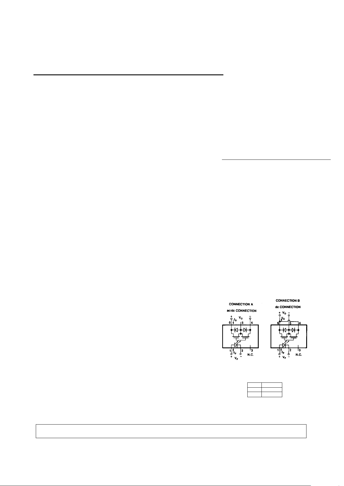
Connection A, as shown in the
schematic, allows the relay to
switch either ac or dc loads.
Connection B, with the polarity
and pin configuration as indicated
in the schematic, allows the relay
to switch dc loads only. The
advantage of Connection B is that
the on-resistance is significantly
reduced, and the output current
capability increases by a factor of
two.
The electrical and switching characteristics of the HSSR-8060 are
specified from -40°C to +85°C.
Features
• Compact Solid-State
Bidirectional Switch
• Normally-Off Single-Pole
Relay Function (1 Form A)
• 60 V Output Withstand
Voltage in Both Polarities at
25°C
• 0.75/1.5 Amp Current
Ratings (See Schematic for
Connections A & B)
• Low Input Current; CMOS
Compatibility
• Very Low On-resistance:
0.4 Ω Typical at 25°C
• ac/dc Signal and Power
Switching
• Input-to-Output Momentary
Withstand Insulation
Voltage: 2500 Vac, 1 Minute
• 16-kV ESD Immunity: MILSTD-883, Method 3015
• IEEE Surge Withstand
Capability (IEEE STD
472-1974)
• CSA Approved
• UL 508 Approved
Applications
• Programmable Logic
Controllers
CAUTION: It is advised that normal static precautions be taken in handling and assembly of this component to
prevent damage and/or degradation which may be induced by ESD.
Functional Diagram
TRUTH TABLE
(POSITIVE LOGIC)
LED
ON
OFF
OUTPUT
L
H
H
5965-3575E
Page 2
1-442
Selection Guide
Maximum Maximum Maximum
6-Pin DIP 4-Pin DIP Maximum ON Output Output Hermetic
(300 Mil) (300 Mil) Speed Resistance Voltage Current Minimum 8-Pin
Single Dual t(ON) R(ON) VO(off) Io(ON) Input Single
Channel Channel msec
Ω V mA Current Channel
Package Package 25
°C25°C25°C25°C mA Packages
HSSR-8400
[1]
0.95 10 400 150 5
HSSR-8060 1.4 0.7 60 750 5
HSSR-8200
[1]
1.5 200 200 40 1
6 1 90 800 5 HSSR-7110
[1]
Note:
1. Technical data are on separate HP publication.
Ordering Information
Specify part number followed by Option Number (if desired).
HSSR-8060#XXX
300 = Gull Wing Surface Mount Lead Option
500 = Tape/Reel Package Option (1 k min.)
Option data sheets available. Contact your Hewlett-Packard sales representative or authorized distributor for
information.
Schematic
I
F
V
F
1
2
+
–
6
SWITCH
DRIVER
5
4
Page 3
1-443
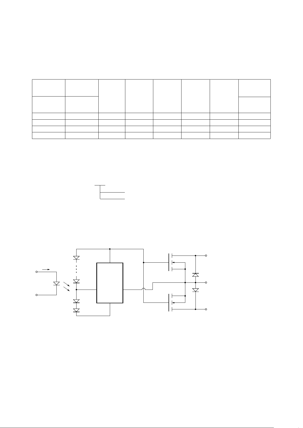
Outline Drawing
6-pin DIP Package (HSSR-8060)
9.40 (0.370)
9.90 (0.390)
PIN
ONE
DOT
HP RXXXX
YYWW
TYPE
NUMBER
DATE CODE
2.16 (0.085)
2.54 (0.100)
2.28 (0.090)
2.80 (0.110)
0.51 (0.020) MIN.
0.45 (0.018)
0.65 (0.025)
4.70 (0.185) MAX.
2.92 (0.115) MIN.
6.10 (0.240)
6.60 (0.260)
0.20 (0.008)
0.33 (0.013)
5° TYP.
7.36 (0.290)
7.88 (0.310)
DIMENSIONS IN MILLIMETERS AND (INCHES).
56
321
1.78 (0.070) MAX.
4
Page 4
1-444
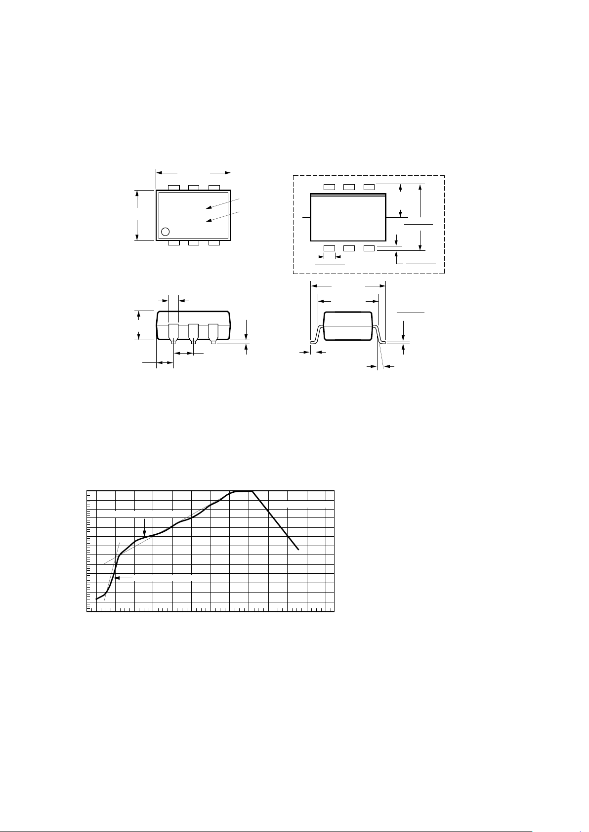
240
∆T = 115°C, 0.3°C/SEC
0
∆T = 100°C, 1.5°C/SEC
∆T = 145°C, 1°C/SEC
TIME – MINUTES
TEMPERATURE – °C
220
200
180
160
140
120
100
80
60
40
20
0
260
123 456789101112
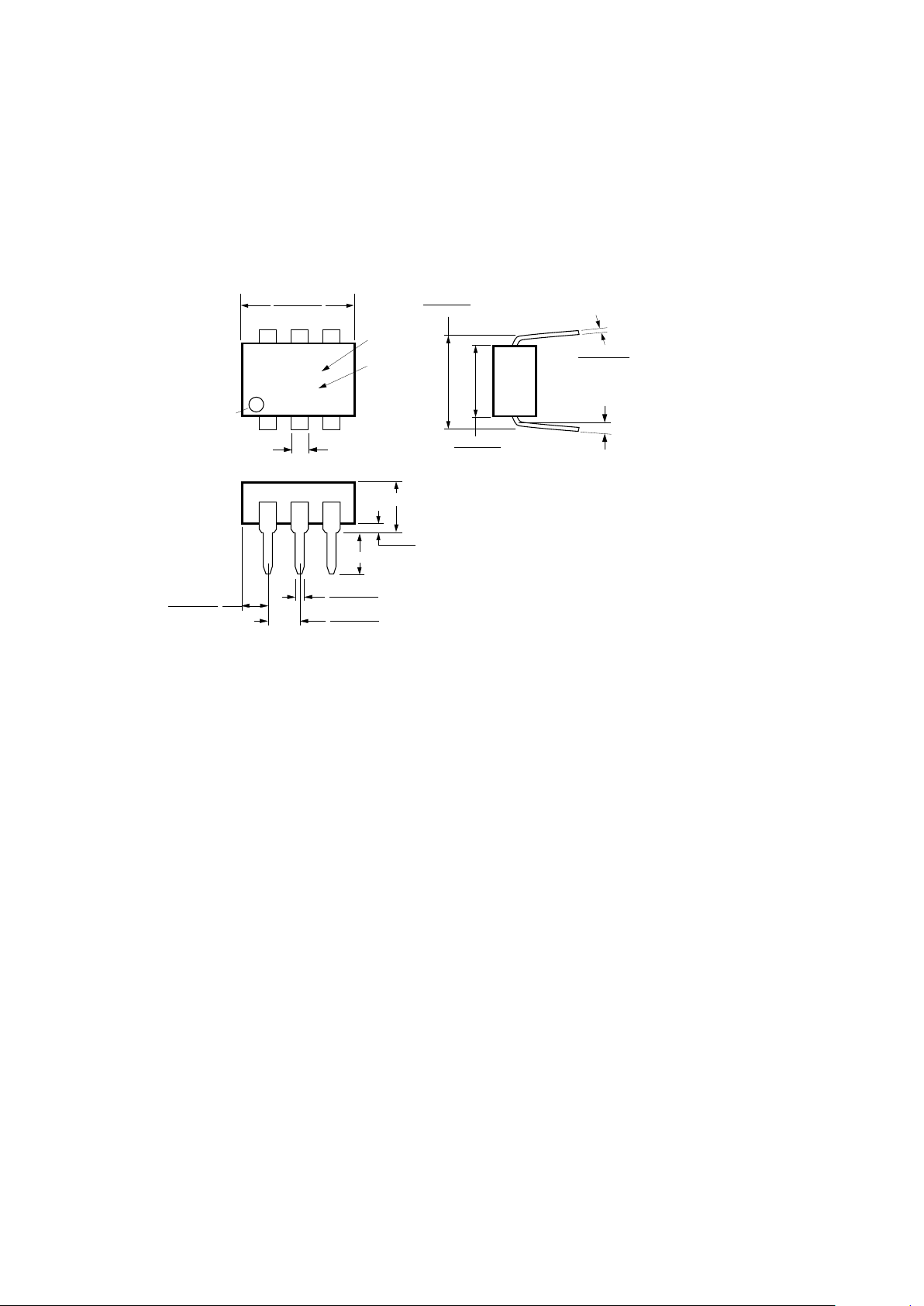
6-Pin Device Outline Drawing Option #300 (Gull Wing Surface Mount)
Thermal Profile (Option #300)
Regulatory Information
The HSSR-8060 has been
approved by the following
organizations:
UL
Recognized under UL 508,
Component Recognition Program,
Industrial Control Switches, File
E142465.
CSA
Approved under CAN/CSA-C22.2
No. 14-95, Industrial Control
Equipment, File LR 87683.
Figure 1. Maximum Solder Reflow Thermal Profile.
(Note: Use of non-chlorine activated fluxes is recommended.)
4.19
(0.165)
2.29
(0.090)
2.54
(0.100)
TYP.
0.635 ± 0.130
(0.025 ± 0.005)
9.65 ± 0.25
(0.380 ± 0.010)
7.62 ± 0.25
(0.300 ± 0.010)
0.635 ± 0.25
(0.025 ± 0.010)
12° NOM.
0.20 (0.008)
0.30 (0.013)
1.78
(0.070)
MAX.
9.65 ± 0.25
(0.380 ± 0.010)
6.35 ± 0.25
(0.250 ± 0.010)
DIMENSIONS IN mm (INCHES)
TOLERANCES: xx.xx = 0.01
xx.xxx = 0.001
(unless otherwise specified)
LEAD COPLANARITY
MAXIMUM: 0.102 (0.004)
[3] [5]
1.194 (0.047)
1.778 (0.070)
4.826
(0.190)
TYP.
9.398 (0.370)
9.906 (0.390)
MAX.
PAD LOCATION (FOR REFERENCE ONLY)
0.381 (0.015)
0.635 (0.025)
HP RXXXX
YYWW
TYPE NUMBER
DATE CODE
Page 5

1-445
Insulation and Safety Related Specifications
Parameter Symbol Value Units Conditions
Min. External Air Gap L(IO1) 7.0 mm Measured from input terminals to output
(External Clearance) terminals, shortest distance through air
Min. External Tracking Path L(IO2) 8.5 mm Measured from input terminals to output
(External Creepage) terminals, shortest distance path along body
Min. Internal Plastic Gap 0.5 mm Through insulation distance, conductor to
(Internal Clearance) conductor, usually the direct distance
between the photoemitter and photodetector
inside the optocoupler cavity
Tracking Resistance CTI 200 V DIN IEC 112/VDE 0303 PART 1
(Comparative Tracking Index)
Isolation Group IIIa Material Group (DIN VDE 0110, 1/89, Table 1)
Option 300 – surface mount classification is Class A in accordance with CECC 00802.
Absolute Maximum Ratings
Storage Temperature ................................................... -55°C to+125°C
Operating Temperature - TA.......................................... -40°C to +85°C
Case Temperature - TC.......................................................... +105°C
[1]
Average Input Current - IF............................................................ 20 mA
Repetitive Peak Input Current - IF............................................... 40 mA
(Pulse Width ≤ 1 ms; duty cycle ≤ 50%)
Transient Peak Input Current - IF............................................... 100 mA
(Pulse Width ≤ 200 µs; duty cycle ≤ 1%)
Reverse Input Voltage - VR................................................................3 V
Input Power Dissipation .............................................................. 40 mW
Output Voltage (TA = 25°C)
Connection A - VO......................................................... -60 to +60 V
Connection B - VO............................................................. 0 to +60 V
Average Output Current - Figure 3 (TA = 25°C, TC ≤ 70°C)
Connection A - IO.....................................................................0.75 A
Connection B - IO.....................................................................1.50 A
Single Shot Peak Output Current
(100 ms pulse width, TA = 25°C, IF = 10 mA)
Connection A - IO.................................................................... 3.75 A
Connection B - IO...................................................................... 7.0 A
Output Power Dissipation ..................................................... 750 mW
[2]
Lead Solder Temperature .... 260°C for 10 S (1.6 mm below seating plane)
Infrared and Vapor Phase Reflow Temperature
(Option #300) ......................................... See Fig. 1, Thermal Profile
Thermal Resistance
Typical Output MOSFET Junction
to Case – θJC = 55°C/W
Demonstrated ESD
Performance
Human Body Model: MIL-STD-
883 Method 3015.7 - 16 kV
Machine Model: EIAJ 1988.3.28
Version 2), Test Method 20,
Condition C – 1200 V
Surge Withstand
Capability
IEEE STD 472-1974
Page 6

1-446
DC Electrical Specifications
For -40oC ≤ TA ≤ +85°C unless otherwise specified. All Typicals at TA = 25°C.
Connec-
Parameter tion Sym. Min. Typ. Max. Units Test Conditions Fig. Notes
Output A |V
O(OFF)
|60 V VF = 0.8 V, IO = 250 µA, 5
Withstand TA = 25°C
Voltage 55 VF = 0.8 V, IO = 250 µA
AR
(ON)
0.4 0.7 Ω 6,7 3
B 0.1 0.2
A 1.6 IF = 10 mA, IO = 750 mA
B 0.4
Output A I
O(OFF)
10
-4
1.0 µAVF = 0.8 V, VO = 60 V, 13
Leakage TA = 25°C
Current
Output Off- A C
(OFF)
135 pF VF = 0.8 V, VO = 25 V, 14
Capacitance f = 1 MHz
Output Off- A |VOS|1 µVIF = 5 mA, IO = 0 mA 18 4
set Voltage
Input Reverse V
R
3VI
R
= 100 µA
Breakdown
Voltage
Input V
F
1.3 1.6 1.85 V IF = 10 mA, TA = 25°C15
Forward
Voltage
Input Diode ∆VF/∆T
A
-1.3 mV/oCIF = 10 mA
Temperature
Coefficient
Input C
IN
72 pF VF = 0 V, f = 1 MHz
Capacitance
Recommended Operating Conditions
Parameter Symbol Min. Max. Units
Input Current (ON) I
F(ON)
520mA
Input Voltage (OFF) V
F(OFF)
0 0.8 Volt
Operating Temperature T
A
-40 +85 °C
Output Voltage
Connection A V
O(OFF)
-55 55 Volt
Connection B 0 55
Output Current
Connection A I
O(ON)
-0.75 0.75 A
Connection B -1.5 1.5
Output OnResistance
(pulse duration ≤ 30 ms)
IF = 10 mA, IO = 750 mA
(pulse duration ≤ 30 ms),
TA = 25oC
Page 7

1-447
Switching Specifications
For -40°C ≤ TA ≤ +85°C with Connection A, unless otherwise specified. All Typicals at TA = 25°C.
Parameter Symbol Min. Typ. Max. Units Test Conditions Fig. Notes
Turn On Time t
ON
0.93 1.4 ms IF = 10 mA, VDD = 60 V, 2,8, 7
IO = 750 mA, TA = 25°C 9,10,
1.8 ms IF = 10 mA, VDD = 55 V,
IO = 750 mA
Turn Off Time t
OFF
0.013 0.1 ms IF = 10 mA, VDD = 60 V, 2,8,
IO = 750 mA, TA = 25°C 11,12,
0.1 ms IF = 10 mA, VDD = 55 V,
IO = 750 mA
Output |dVO/dt| 1000 V/µsV
(peak)
= 60 V, RM ≥ 1 MΩ,16
Transient CM = 1000 pF, TA = 25°C
Rejection
Input-Output |dV
I-O
/dt| 2500 V/µsVDD = 5 V, V
I-O(peak)
= 1000 V, 17
Transient RL = 1 kΩ, CL = 25 pF,
Rejection TA = 25°C
Package Characteristics
For 0°C ≤ TA ≤ 70°C, unless otherwise specified. All typicals at TA = 25°C.
Parameter Symbol Min. Typ. Max. Units Test Conditions Fig. Notes
Input-Output V
ISO
2500 V rms RH ≤ 50%, t = 1 min, TA = 25°C 5,6
Momentary Withstand Voltage*
Resistance R
I-O
100 GΩ V
I-O
= 500 Vdc, t = 1 min, 5
Input-Output RH = 45%
Capacitance C
I-O
1.0 pF V
I-O
= 0 V, f = 1 MHz 5
Input-Output
*The Input-Output Momentary Withstand Voltage is a dielectric voltage rating that should not be interpreted as an input-output
continuous voltage rating. For the continuous voltage rating refer to the VDE 0884 Insulation Characteristics Table (if applicable),
your equipment level safety specification, or HP Application Note 1074, “Optocoupler Input-Output Endurance Voltage.”
20,21
Notes:
1. The case temperature, TC, is measured
at the center of the bottom of the
package.
2. For derating, see Figure 4. The output
power PO derating curve is obtained
when the part is handling the maximum
average output current IO as shown in
Figure 3.
3. During the pulsed RON measurement (I
O
duration ≤ 30 ms), ambient (TA) and
case temperature (TC) are equal.
4. VOS is a function of IF, and is defined
between pins 4 and 6, with pin 4 as the
reference. VOS must be measured in a
stable ambient (free of temperature
gradients).
5. Device considered a two terminal
device: pins 1, 2, and 3 shorted
together and pins 4, 5, and 6 shorted
together.
6. This is a momentary withstand proof
test. These parts are 100% tested in
production at 3000 V rms, one second.
7. For a faster turn-on time, the optional
peaking circuit shown in Figure 2 may
be implemented.
20,21
Page 8

1-448
Figure 5. Normalized Typical Output
Withstand Voltage vs. Temperature.
Figure 7. Typical On State Output I-V
Characteristics.
Figure 2. Recommended Input Circuit.
Figure 6. Normalized Typical Output
Resistance vs. Temperature.
Figure 3A. Maximum Average Output
Current Rating vs. Ambient
Temperature.
Figure 3B. Maximum Average Output
Current Rating vs. Case Temperature.
Figure 4. Output Power Derating vs.
Case Temperature.
Page 9

1-449
Figure 8. Switching Test Circuit for tON, t
OFF
.
Figure 9. Typical Turn On Time vs.
Temperature.
Figure 10. Typical Turn On Time vs.
Input Current.
Figure 11. Typical Turn Off Time vs.
Temperature.
Figure 12. Typical Turn Off Time vs.
Input Current.
Page 10

1-450
CONNECTION A
V
F(OFF)
= 0.8 V
V
O(OFF)
= 55 V
Figure 13. Typical Output Leakage vs.
Temperature.
Figure 14. Typical Output
Capacitance vs. Output Voltage.
Figure 16. Output Transient Rejection Test Circuit.
Figure 15. Typical Input Forward
Current vs. Input Forward Voltage.
Page 11

1-451
Figure 17. Input-Output Transient Rejection Test Circuit.
Figure 18. Voltage Offset Test Setup. Figure 19. Thermal Model.
Tjo= LED JUNCTION TEMPERATURE
T
11
= FET 1 JUNCTION TEMPERATURE
T
12
= FET 2 JUNCTION TEMPERATURE
T
jd
= FET DRIVER JUNCTION TEMPERATURE
T
C
= CASE TEMPERATURE ( MEASURED AT
CENTER OF PACKAGE BOTTOM)
T
A
= AMBIENT TEMPERATURE (MEASURED
15 cm AWAY FROM THE PACKAGE)
θ
CA
= CASE-TO-AMBIENT THERMAL RESISTANCE
ALL THERMAL RESISTANCE VALUES ARE IN
°C/W.
Page 12

1-452
Figure 20. Turn On Time Variation with High Temperature
Operating Life.
Figure 21. Turn On Time Variation with Temperature Cycling.
Page 13

1-453
related by the expression
RSS=PO(max)/(IO(max))2 from
which RSS can be calculated.
Staying within the safe area
assures that the steady state
junction temperatures remain less
than 125°C. As an example, for a
case temperature of 100°C,
Figure 4 shows that the output
power dissipation should be
limited to less than 0.5 watts. A
check with Figure 3B shows that
the output current should be
limited to less than 150 mA. This
yields an RSS of 22 Ω.
Applications Information
Thermal Model
The steady state thermal model
for the HSSR-8400 is shown in
Figure 19. The thermal resistance
values given in this model can be
used to calculate the temperatures at each node for a given
operating condition. The thermal
resistances between the LED and
other internal nodes are very
large in comparison with the
other terms and are omitted for
simplicity. The components do,
however, interact indirectly
through θCA, the case-to-ambient
thermal resistance. All heat
generated flows through θCA,
which raises the case temperature
TC accordingly. The value of θ
CA
depends on the conditions of the
board design and is, therefore,
determined by the designer.
The typical value for each output
MOSFET junction-to-case thermal
resistance is specified as 55°C/W.
This is the thermal resistance
from one MOSFET junction to the
case when power is dissipated
equally in the MOSFETs. The
power dissipation in the FET
Driver is negligible in comparison
to the MOSFETs.
On-Resistance and Derating
Curves
The output on-resistance, RON,
specified in this data sheet, is the
resistance measured across the
output contact when a pulsed
current signal (IO = 150 mA) is
applied to the output pins. The
use of a pulsed signal (≤ 30 ms)
implies that each junction temperature is equal to the ambient and
case temperatures. The steadystate resistance, RSS, on the other
hand, is the value of the
resistance measured across the
output contact when a DC current
signal is applied to the output
pins for a duration sufficient to
reach thermal equilibrium. R
SS
includes the effects of the temperature rise of each element in
the thermal model.
Derating curves are shown in
Figures 3 and 4. Figure 3 specifies the maximum average output
current allowable for a given
ambient or case temperature.
Figure 4 specifies the output
power dissipation allowable for a
given case temperature. Above a
case temperature of 93°C, the
maximum allowable output
current and power dissipation are
Turn On Time Variation
For applications which are
sensitive to turn on time, the
designer should refer to Figures
20 and 21. These figures show
that although there is very little
variation in tON within most of the
population, a portion of the
distribution will vary with use.
The optional peaking circuit
shown in Figure 2 can be used to
reduce the total turn on time and,
consequently, any associated
variation.
 Loading...