

Page 1
Infrared IrDA® Compliant
Transceiver
Technical Data
H
HSDL-1000
Features
• Low Cost Infrared Data Link
• Guaranteed to Meet IrDA
Physical Layer Specifications
1 cm to 1 Meter Operating
Distance
30° Viewing Angle
2.4 KBd to 115.2 KBd Data
Rate
• Daylight Cancellation
• Easily Implemented Direct
Connection to Various I/O
Chips
• Small Form Factor
• Several Lead and Shipping
Configurations Available
• Excellent EMI Immunity
(> 10 V/m)
Applications
• Data Comm: Serial Data
Transfer Between:
Notebook Computers
Subnotebooks
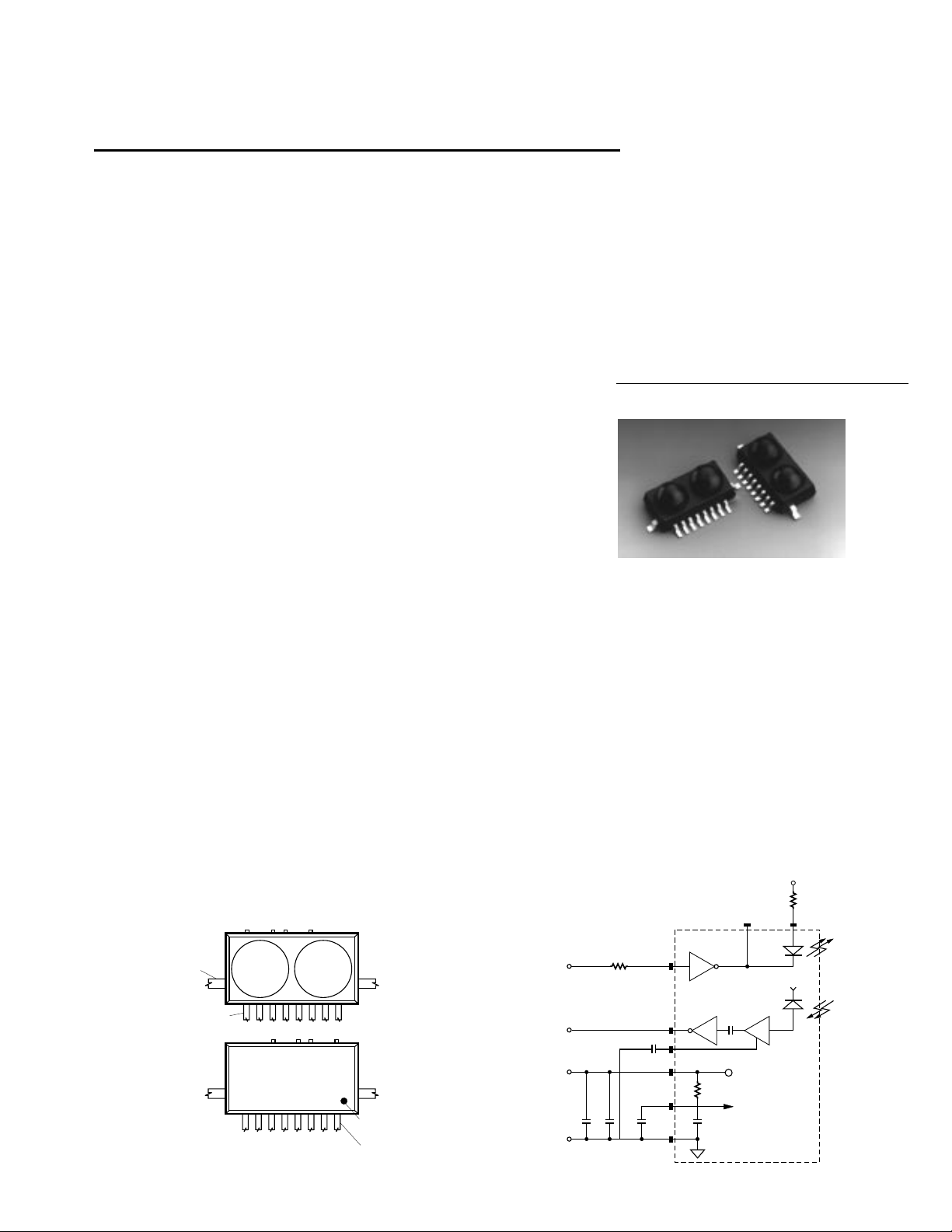
Schematic
BUTTRESS
LEAD*
PIN ONE
HP 1000
YYWW
* SIDE BUTTRESS LEADS ARE FOR MECHANICAL STABILITY AND
SHOULD NOT BE CONNECTED TO ANY ELECTRICAL POTENTIAL.
5964-9641E
Desktop PCs
PDAs
Printers
Other Peripheral Devices
• Telecom:
Modem, Fax, Pager, Phone
• Industrial:
Data Collection Devices
• Medical:
Patient and Pharmaceutical
Data Collection
Description:
The HSDL-1000 serial infrared
module performs low cost, low
power, point-to-point, through the
air data transfer in a serial, halfduplex mode.
The module has been designed to
the IrDA (Infrared Data Association) Physical Layer Specifications. The module is designed to
TXD
RXD
V+
PIN ONE
INDICATOR
PIN ONE
GND
operate from 0 to 1 meter at a
data rate of 115.2 Kbd per second
at a 30° viewing angle.
The HSDL-1000 contains a high
speed, high efficiency TS AlGaAs
875 nm LED, a PIN Silicon photodiode and an integrated circuit.
The IC contains an LED driver,
amplifiers and a quantizer.
The module is designed to interface directly with selected I/O
chips that incorporate logic which
performs pulse width modulation/
demodulation.
V+
R
LED
LED C LED A
R
I
TXD
COMPARATOR
RXD
CX1
V
CC
CX2
CX2CX3CX4
GND
LED
PHOTODIODE
+
V
PIN
V
PIN
4-33
Page 2
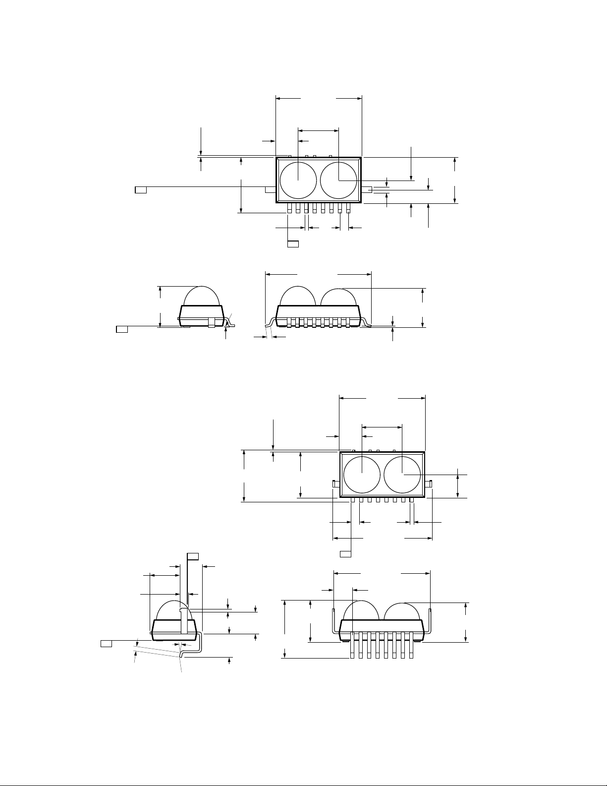
Package Dimensions
Option X01*
0.43
(0.017)
MAX.
3.4 ± 0.25
(0.14 ± 0.01)
12.95 (0.51)
13.45 (0.53)
6.4 ± 0.25
(0.25 ± 0.01)
3.4 ± 0.25
(0.14 ± 0.01)
Option X02*
-A-
-B-
6.2 ± 0.25
(0.24 ± 0.01)
8.54 ± 0.15
(0.336 ± 0.01)
(0.020 ± 0.003)
5.0° (10x)
DIMENSIONS IN MILLIMETERS (INCHES).
0.51 ± 0.08
MAX.
1 2345678
(8x)
-C-
0.6 ± 0.25
(0.02 ± 0.01)
0.43
MAX.
(0.017)
3.4 ± 0.25
(0.14 ± 0.01)
16.61 ± 0.15
(0.654 ± 0.01)
(10x)
0.9 ± 0.25
(0.04 ± 0.01)
1.27 ± 0.15
(0.050 ± 0.01)
0.13 ± 0.08
(0.005 ± 0.003)
13.2 ± 0.25
(0.52 ± 0.01)
6.4 ± 0.25
(0.25 ± 0.01)
(7x)
(0.08 ± 0.01)
5.93 ± 0.25
(0.23 ± 0.01)
6.9 ± 0.25
(0.27 ± 0.01)
1.9 ± 0.25
3.4 ± 0.25
(0.14 ± 0.01)
0.51 ± 0.08
(0.020 ± 0.003)
5.93 ± 0.25
(0.23 ± 0.01)
(8x)
4.56 ± 0.15
(0.180 ± 0.01)
1.28 ± 0.15
(0.050 ± 0.01)
-A-
0.60 ± 0.25
(0.02 ± 0.01)
5.0° (8x)
8.05 ± 0.15
(0.317 ± 0.01)
-B-
(0.132 ± 0.01)
3.80 ± 0.15
(0.150 ± 0.01)
COPLANARITY ± 0.05 mm (0.002 INCHES).
MAX.
3.36 ± 0.15
0.50 ± 0.13
(0.020 ± 0.005)
3.28 ± 0.15
(0.129 ± 0.01)
DIMENSIONS IN MILLIMETERS (INCHES).
6.9 ± 0.25
(0.27 ± 0.01)
1.27 ± 0.15
(0.050 ± 0.01)
6.2 ± 0.25
(0.24 ± 0.01)
8.88 ± 0.15
(0.349 ± 0.01)
(7x)
1 2345678
15.39 ± 0.15
(0.606 ± 0.01)
-C-
15.13 ± 0.15
(0.596 ± 0.01)
3.12 ± 0.15
(0.123 ± 0.01)
Note:
The -B- datum is formed by the two highest points of the combined surface formed by this surface and the corresponding surface of the
same lead on the opposite side of the package.
*X position indicates packaging. 0 = tape and reel, 1 = JEDEC standard tray.
4-34
Page 3
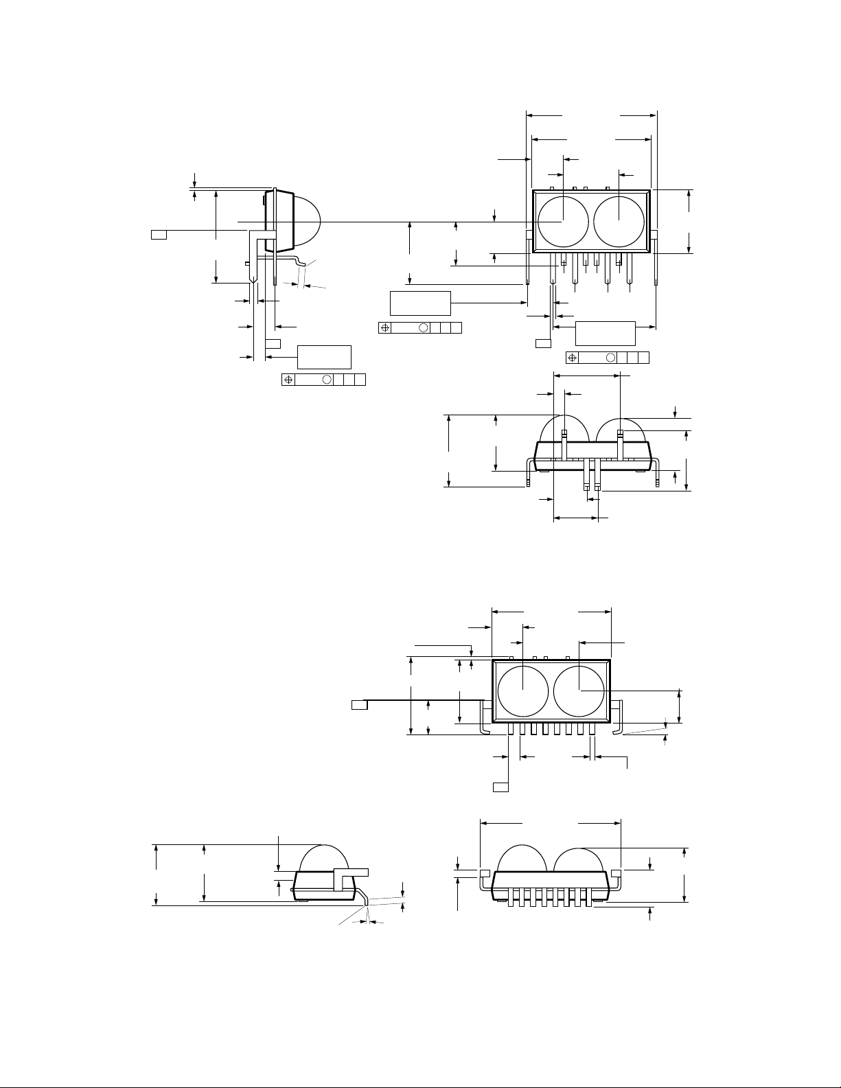
Package Dimensions (continued)
Option X03*
0.43 (0.02) MAX.
-B-
11.0 ± 0.13
(0.43 ± 0.01)
-A-
COPLANARITY
OF SURFACE MOUNT
LEADS TO BE
WITHIN 0.3 mm.
0.76 ± 0.15
(0.03 ± 0.01)
2.54 ± 0.15
(0.100 ± 0.01)
1.39 ± 0.15
(0.05 ± 0.01)
0.6 ± 0.25
(0.02 ± 0.01)
A BCS.30∅
7.11 ± 0.15
(0.280 ± 0.01)
2.79 ± 0.15
(0.110 ± 0.01)
3.4 ± 0.25
(0.14 ± 0.01)
(0.135 ± 0.01)
4.95 ± 0.15
(0.195 ± 0.01)
(0.020 ± 0.01)
A BCS.30∅
3.43 ± 0.15
0.51 ± 0.15
1.27 ± 0.15
(0.050 ± 0.01)
-C-
14.73 ± 0.15
(0.580 ± 0.01)
13.2 ± 0.25
(0.52 ± 0.01)
6.4 ± 0.25
(0.25 ± 0.01)
11.68 ± 0.15
(0.460 ± 0.01)
A BCS.30∅
7.62 ± 0.15
(0.300 ± 0.01)
5.9 ± 0.25
(0.23 ± 0.01)
6.9 ± 0.25
(0.27 ± 0.01)
Option X04*
DIMENSIONS IN MILLIMETERS (INCHES).
0.43 (0.02) MAX.
8.75 ± 0.15
(0.345 ± 0.01)
-B-
0.90 ± 0.25
(0.04 ± 0.01)
7.87 ± 0.15
(0.310 ± 0.01)
3.43 ± 0.25
(0.14 ± 0.010)
MAX.
3.84
(0.151)
1.27 ± 0.15
(0.050 ± 0.01)
(0.24 ± 0.01)
6.86 ± 0.25
(0.27 ± 0.01)
6.2 ± 0.25
3.81 ± 0.15
(0.150 ± 0.01)
1 2345678
(7x)
-C-
(0.626 ± 0.01)
13.21 ± 0.25
(0.52 ± 0.01)
15.89 ± 0.15
5.08 ± 0.15
(0.200 ± 0.01)
6.35 ± 0.25
(0.25 ± 0.010)
0.51 ± 0.08
(0.020 ± 0.003)
6.75 ± 0.15
(0.266 ± 0.01)
3.43 ± 0.25
(0.14 ± 0.010)
5.0° ± 3.5°
(8x)
6.79 ± 0.25
(0.27 ± 0.01)
6.22 ± 0.25
(0.24 ± 0.01)
APPROX.
COPLANARITY
± 0.076 mm (0.003 INCHES).
CG
0.61 ± 0.25
(0.02 ± 0.01)
0.76 ± 0.08
5.00°
DIMENSIONS IN MILLIMETERS (INCHES).
(0.030 ± 0.003)
(2x)
(0.162 ± 0.006)
5.93 ± 0.25
(0.23 ± 0.01)
4.12 ± 0.15
Note:
The -B- datum is formed by the two highest points of the combined surface formed by this surface and the corresponding surface of the
same lead on the opposite side of the package.
*X position indicates packaging. 0 = tape and reel, 1 = JEDEC standard tray.
4-35
Page 4
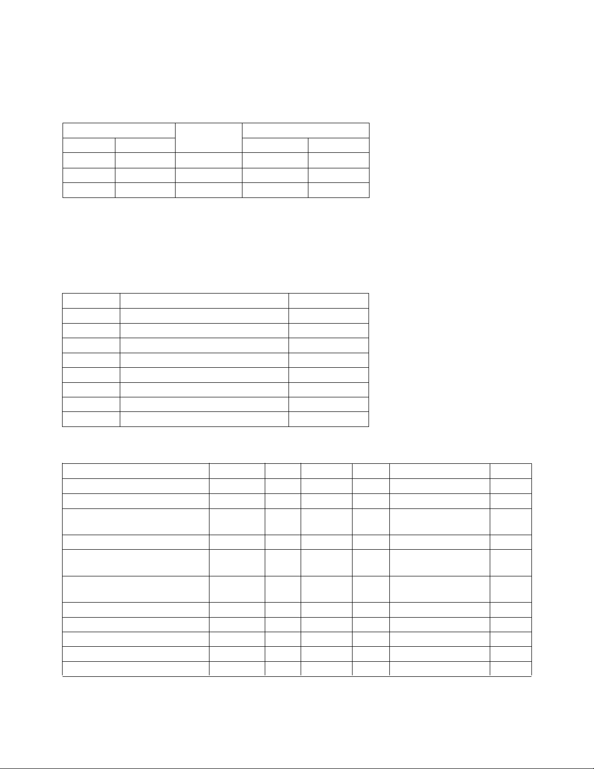
Truth Table
Inputs Outputs
TXD EI
V
IH
V
IL
V
IL
X = Don’t care.
Notes:
1. EI – received in band light intensity present at detector surface.
2. Logic Low is a pulsed response. A receiver output low state VOL (RXD) is not indefinitely
maintained, but is instead a pulsed response. The output low state is maintained for a
duration dependent on the incident bit pattern and the incident intensity (EI).
[1]
LED LEDA RXD
X ON Low Low
EI
EI
H
L
OFF High Low
OFF High High
[2]
[2]
Pinout
Pin Description Symbol
1 Daylight Cancellation Capacitor CX1
2 PIN Bypass Capacitor CX2
3 Supply Voltage V
4 Receiver Data Output RXD
5 Ground Gnd
6 Transmitter Data Input TXD
7 LED Cathode LEDC
8 LED Anode LEDA
CC
Absolute Maximum Ratings
Parameter Symbol Min. Max. Units Conditions Fig.
Storage Temperature T
Operating Temperature T
S
A
Lead Solder Temperature 260 C For 10 s (1.6 mm Reflow
Average LED Current I
Repetitive Pulsed LED Current I
Peak LED Current I
LED Anode Voltage V
LED Cathode Voltage V
Supply Voltage V
Transmitter Data Input Voltage V
Receiver Data Output Voltage V
(DC) 100 mA
LED
(PK) 500 mA ≤ 90 µs Pulse Width,
LED
(RP) 1.0 A ≤ 2 µs Pulse Width,
LED
LEDA
LEDC
CC
TXD
RXD
-20 85 C
070C
-0.5 7.0 V
-0.5 V
LEDA
V
0 7.0 V
-0.5 5.5 V
-0.5 VCC + 0.5 V
below seating plane) Profile
≤ 20% Duty Cycle
≤ 10% Duty Cycle
4-36
Page 5
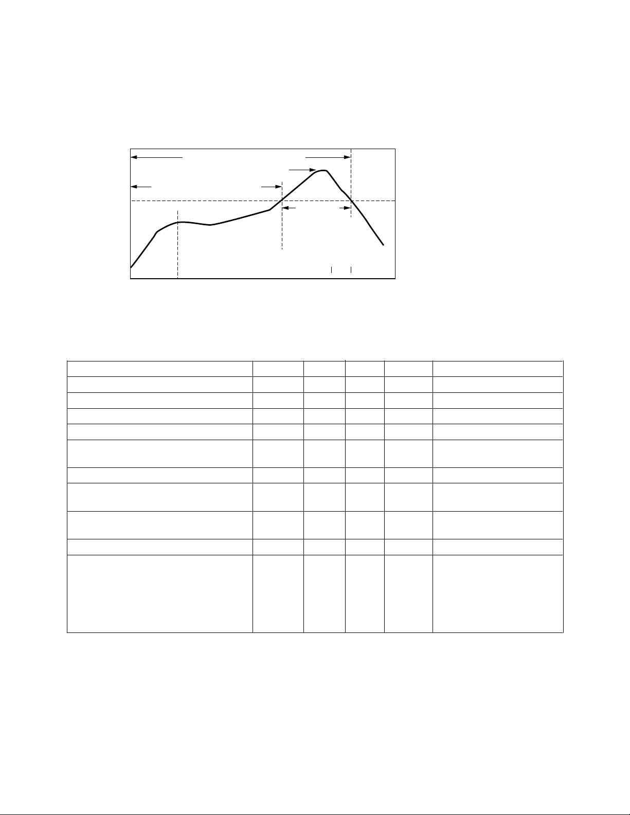
Infrared Reflow Profile
300
250
200
150
100
TEMPERATURE – °C (T)
50
0
t1 = 8 ± 1 MINS. (SOLDER JOINT)
185 °C
0
t2 = 11.5 ± .5 MINS. (SOLDER JOINT)
T (MAX.) = 250 °C OR 235 °C (+5-0) °C
ANY PART OF COMPONENT BODY
3.5 ± .5 MINS.
(SOLDER JOINT)
T > 120 °C FOR t
GREATER THAN 2.5 MINS.
(SOLDER JOINT)
dT/dt < 3 °C/SEC.
2 4 6 8 10 12 14
TIME (t)
Recommended Operating Conditions
Parameter Symbol Min. Max. Units Conditions
Operating Temperature T
Supply Voltage V
Logic High Transmitter Input Voltage V
A
CC
(TXD) 2.5 5.5 V
IH
Logic Low Transmitter Input Voltage VIL (TXD) 0.0 0.3 V
Logic High Receiver Input Irradiance EI
H
(870 nm)
Logic Low Receiver Input Irradiance EI
LED (Logic High) Current Pulse I
L
LEDA
Amplitude daylight filters
Receiver Set-up Time 10 ms For full sensitivity after
Signal Rate 2.4 116 Kp/s
Ambient Light See IrDA Serial Infrared
0° 70° C
4.5 5.5 V
0.0036 500 mW/cm2For in-band signals*
0.3 µW/cm2For in-band signals*
250 mA For one metre links with
transmitting
Physical Layer Link Specification, Appendix A for
ambient levels. See Rx
TH+ section at the end
of this data sheet also.
*Note: An in-band optical signal is a pulse/sequence where the peak wavelength, λp, is defined as 850 nm ≤ λp ≤ 900 nm, the pulse
repetition rate, PRR, is defined as 2.4 Kp/s ≤ PRR ≤ 115.2 Kp/s and the pulse width, PW, is defined as 1.6 s ≤ PW ≤ (3/16)/PRR.
4-37
Page 6
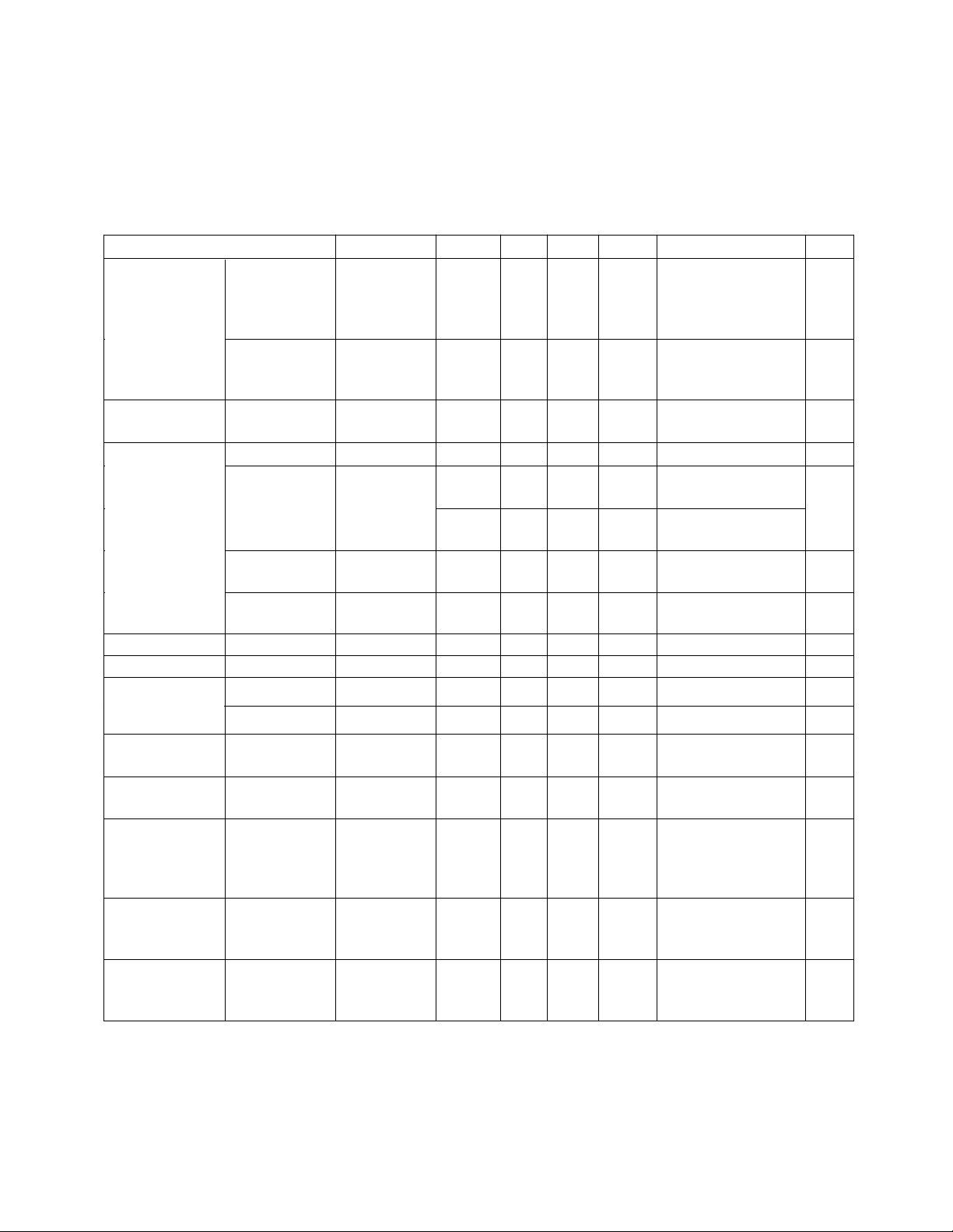
Electrical & Optical Specifications
Specifications hold over the Recommended Operating Conditions unless otherwise noted. Test Conditions represent worse case
values for the parameters under test. Unspecified test condition can be anywhere in their recommended operating range. All typicals
are at 25°C and 5V unless otherwise noted.
Parameter Symbol Min. Typ. Max. Unit Conditions Fig.
Receiver Data Logic Low
[2]
VOL (RXD)
Output Voltage For In-Band
Logic High VOH (RXD) VCC -0.5 V IO = -20 µA,
Effective 0.2 cm
Detector Area
Transmitter Logic Low IE
Radient
Intensity
Logic High IE
Intensity VI = 2.5 V, θ ≤ 30°
Peak λp 875 nm 6
Wavelength
Spectral Line ∆λ1/2 35 nm 6
Half Width
Transmitter Viewing Angle θ 30 60 ° 7
Receiver φ 30 °
Transmitter Logic Low IIL(TXD) -1.0 1.0 µA Gnd ≤ VI ≤ 0.3 V
Data Input
Current
Logic High IIH(TXD) 4.5 mA VI = 2.5 V 1
LED Anode On VON (LEDA) 2.50 V I
State Voltage Tj = 25°C
LED Anode Off ILK (LEDA) 100 µAV
State Leakage VI = 0.3V
Supply Current ICC1 1.1 mA VCC = 5.5, 11
TXD High VI (TXD) = VIH,
Supply Current ICC2 13 mA VCC = 5.5, 1
RXD Low
[2]
Receiver Peak λp 880 nm 9
Sensitivity
Wavelength
[2,3]
0.4 V IO = 0.3 mA
EI ≥ 3.6 µW/cm2;
θ ≤ 15°
For In-Band
EI ≤ 0.3 µW/cm
2
L
H
44 250 mW/SR I
0.3 µW/SR VI ≤ 0.3 V
= 250 mA, 4, 6
LEDA
40 mW/SR I
= 250 mA,
LEDA
2
VI = 2.5 V; θ > 60°
= 250 mA, 1, 3
LEDA
= VCC = 5.5 V,
LEDA
I
= 250 mA,
LED
EI = 0
VI (TXD) = VIL,
EI = 500 mW/cm
2
Notes:
1. EI – received in band light intensity present at detector surface.
2. Pulsed Response – Logic Low is a pulsed response. A receiver output low state VOL (RXD) is not indefinitely maintained but is instead a
pulsed response. The output low state is maintained for a duration dependent on the incident bit pattern and
3. The EI ≥ 3.6 µW/cm2 condition guarantees the IrDA minimum receiver sensitivity of 4.0 µW/cm2 while allowing for 10% light loss
through a cosmetic window placed in front of the HSDL-1000. (See the Rx TH+ section at the end of this data sheet for information
on receiver sensitivity over temperature, and in the presence of ambient light.)
4-38
incident intensity (EI).
Page 7
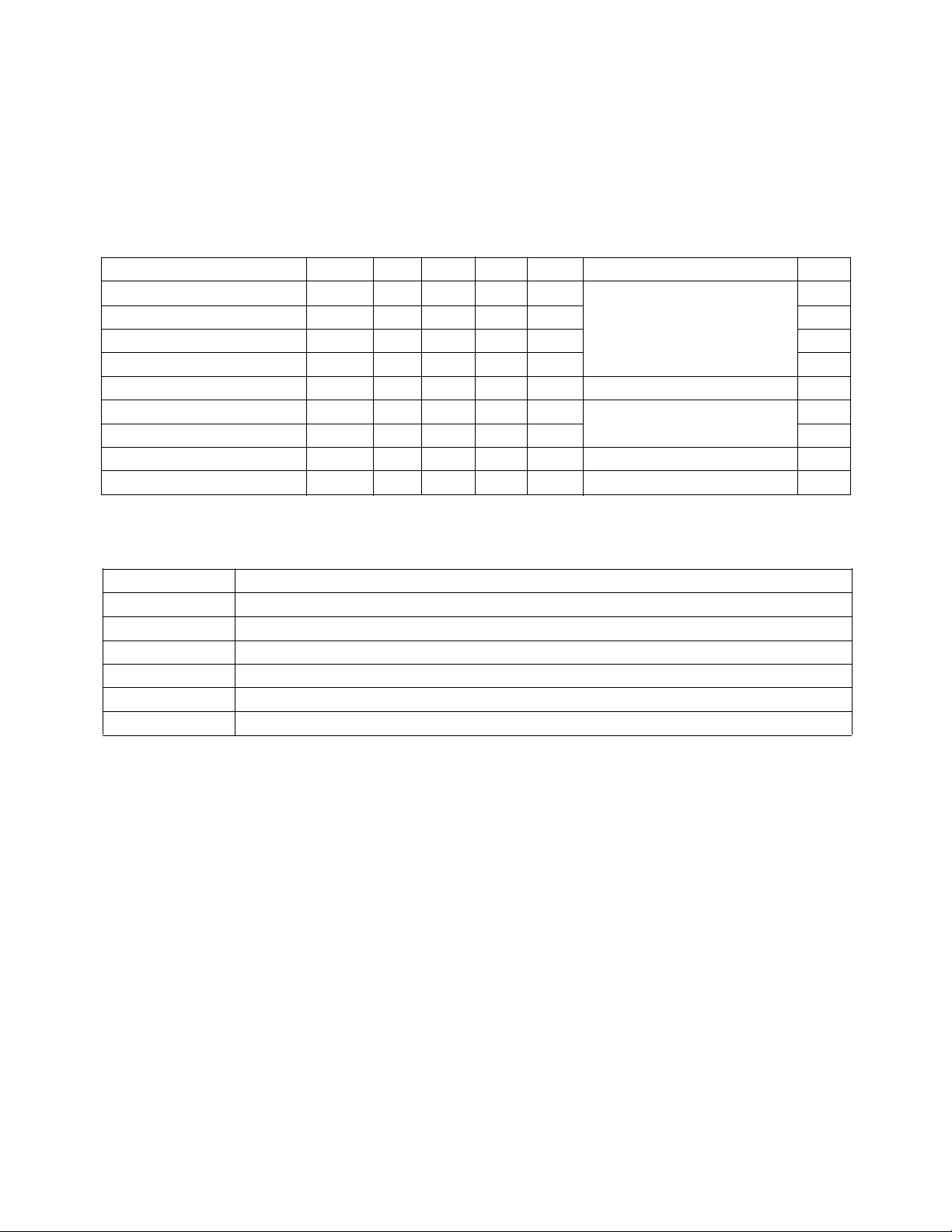
Switching Specifications
Specifications hold over the Recommended Operating Conditions unless otherwise noted. Test Conditions represent worst case
values for the parameters under test. Unspecified test conditions can be anywhere in their recommended operating range. All
typicals are at 25°C and 5V unless otherwise noted.
Parameter Symbol Min. Typ. Max. Units Conditions Fig.
Transmitter Turn On Time 0.1 µsI
= 250 mA, 1.6 µs PW 13, 14
LED
Transmitter Turn Off Time 0.4 1.0 µs
Transmitter Rise Time 0.6 µs
Transmitter Fall Time 0.6 µs
Receiver Turn On Time 0.4 µs EI = 3.6 µW/cm2, 1.6 µs PW 15, 16
Receiver Turn Off Time 5.4 µs EI = 500 mW/cm2, 1.6 µs PW
Receiver Rise Time 1.0 µs
Receiver Fall Time 0.02 µs EI = 3.6 µW/cm2, 1.6 µs PW
Receiver Recovery Time 10 ms
Application Circuit
Component Recommended Value
R
I
R
LED
CX1 0.22 µF ± 10%
CX2 0.4 µF minimum
CX3 0.10 µF ± 22%. Low inductance is critical
CX4 4.7 µF minimum. Larger value is recommended for noisy supplies or environments.
300 Ohms ± 5%
8.0 Ohms maximum
4-39
Page 8
1000
500
250
100
50
10
– LED PULSE CURRENT AMPLITUDE – mA
LEDA
I
234
1
V
– LEDA VOLTAGE – V
LEDA
TA = 25 °C
– LEDA VOLTAGE – V
LEDA
V
5
2.5
I
LEDA
2.4
1.6 µs PW,
3/16 DUTY CYCLE
2.3
2.2
2.1
2.0
0
= 250 mA PULSED
20 40 80
TA – TEMPERATURE – °C
60
100
2.2
I
= 250 mA PULSED
LEDA
1.6 µs PW,
2.1
3/16 DUTY CYCLE
2.0
1.9
– LED FORWARD VOLTAGE – V
F
V
1.8
0
20 40 80
TA – TEMPERATURE – °C
60
100
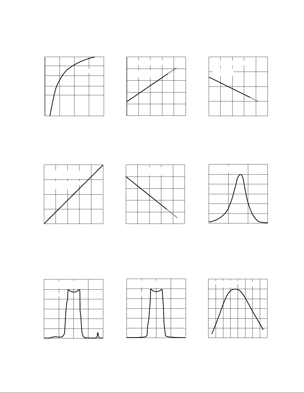
Figure 1. LED Pulse Current
Amplitude vs. LEDA Voltage.
2.0
NORMALIZED TO IE
@ I
= 250 mA
LEDA
1.5
PULSE WIDTH = 1.6 µs
1.0
0.5
0
0
NORMALIZED TRANSMITTED INTENSITY IE
I
LEDA
TO 90 µs.
100 200 400
– LED PULSE AMPLITUDE – mA
300
Figure 4. Transmitted Intensity vs.
LED Pulse Amplitude.
1.2
NORMALIZED TO IE
1.0
TA = 25 °C
0.8
@ I
LEDA
= 250 mA
Figure 2. LEDA Voltage vs.
Temperature.
500
1.2
1.1
1.0
0.9
0.8
0.7
NORMALIZED TRANSMITTED INTENSITY IE
NORMALIZED TO IE
@ I
LEDA
0
20 40 80
TA – TEMPERATURE – °C
Figure 5. Transmitted Intensity vs.
Temperature.
1.2
NORMALIZED TO IE
1.0
0.8
@ I
LEDA
TA = 25 °C
= 250 mA
= 250 mA
60
Figure 3. LED Forward Voltage vs.
Temperature.
100
1.2
NORMALIZED TO IE
1.0
TA = 25 °C
0.8
0.6
0.4
0.2
0
800
NORMALIZED TRANSMITTED INTENSITY IE
@ I
= 250 mA
LEDA
850 900
λ – WAVELENGTH – nm
Figure 6. Transmitted Intensity vs.
Wavelength.
1.2
1.0
0.8
NORMALIZED
TO 880 nm
TA = 25 °C
950
0.6
0.4
0.2
0
-100 100
NORMALIZED TRANSMITTED INTENSITY IE
-50 50
θ – HORIZONTAL TRANSMITTER
VIEWING ANGLE – °
0
Figure 7. Transmitted Intensity vs.
Horizontal Viewing Angle.
4-40
0.6
0.4
0.2
0
-100 100
NORMALIZED TRANSMITTED INTENSITY IE
-50 50
θ – VERTICAL TRANSMITTER
0
VIEWING ANGLE – °
Figure 8. Transmitted Intensity vs.
Vertical Viewing Angle.
0.6
0.4
0.2
0
700 800 900 1100
NORMALIZED RECEIVER RESPONSIVITY
λ – WAVELENGTH – nm
1000
Figure 9. Receiver Responsivity vs.
Wavelength.
Page 9
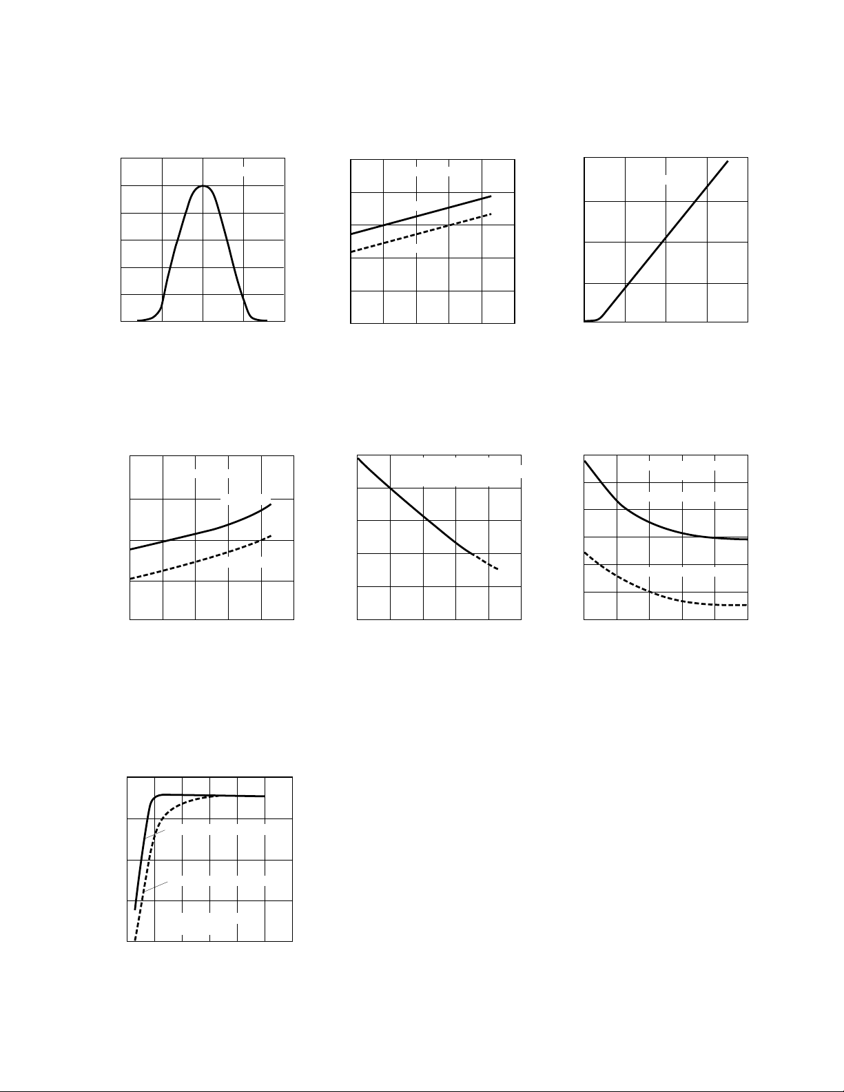
1.2
TA = 25 °C
1.0
0.8
0.6
0.4
0.2
0
-100 100
NORMALIZED RECEIVER RESPONSIVITY
-50 50
ϕ – RECEIVER VIEWING ANGLE – °
0
1.0
0.9
0.8
0.7
0.6
– SUPPLY CURRENT – mA
CC
I
0.5
ILEDA = 250 mA
VCC = 5.5 V
VCC = 4.5 V
40
20 80
TA – TEMPERATURE – °C
600 100
20
TA = 25 °C
15
10
– TRANSMITTER DATA
5
INPUT CURRENT – mA
TXD
I
0
26
V
– TRANSMITTER DATA
TXD
INPUT VOLTAGE – V
408
Figure 10. Receiver Responsivity vs.
Viewing Angle.
2.0
INPUT PW = 1.6 µs
R
1.9
1.8
1.7
– TRANSMITTED PULSE WIDTH – µs
IE
PW
1.6
20 60
40080
TA – TEMPERATURE – °C
= 8 Ω
LED
R
= 2 Ω
LED
Figure 13. Transmitted Pulse Width
vs. Temperature.
6
Figure 11. Supply Current vs.
Temperature.
3.0
2.9
2.8
2.7
2.6
100
2.5
PW(RXD) – RECEIVER OUTPUT PULSE WIDTH – µs
INPUT PW = 1.6 µs
EI INTENSITY = 100 µW/cm2
EI DUTY CYCLE = 20%
20 60
40080
TA – TEMPERATURE – °C
Figure 14. Transmitted Pulse Width
vs. Temperature.
Figure 12. Data Input Current vs.
Data Input Voltage.
100
4.5
4.0
3.5
3.0
2.5
2.0
1.5
PW(RXD) – RECEIVER OUTPUT PULSE WIDTH – µs
EI PULSE WIDTH = 1.6 µs
EI INTENSITY = 100 µW/cm
EI INTENSITY = 3.6 µW/cm
10 20
DUTY CYCLE OF LIGHT PULSE EI – %
Figure 15. Receiver Output Pulse
Width vs. Duty Cycle of Received
Signal.
TA = 25 °C
2
2
1505 25
5
4
3
2
PWEI – RECEIVED LIGHT PULSE WIDTH – µs
PW(RXD) – RECEIVER OUTPUT PULSE WIDTH – µs
EI INTENSITY = 100 µW/cm
EI INTENSITY = 3.6 µW/cm
20% DUTY CYCLE
T
= 25 °C
A
510 25
0
15
20
2
2
30
Figure 16. Receiver Output Pulse
Width vs. Received Light Pulse Width.
4-41
Page 10
Rx TH+ (Receiver OnThreshold)
The maximum receiver onthreshold is equivalent to the
minimum receiver sensitivity.
Both are terms for the amount of
light signal which must be present
at the HSDL-1000 detector in
order to trigger a low pulse on the
receiver output (RXD). The IrDA
Physical Layer Specification
requires a minimum receiver
sensitivity of 4.0 µW/cm2, at a Bit
Error Rate of 10-9, and in the
presence of the 10 klux of
sunlight, 0-1000 lux of fluorescent
light, or 0-1000 lux of incandescent light. The fluorescent and
incandescent specifications
require minimum receiver
sensitivity with 1000 lux incident
onto the horizontal surface of the
IR link. The resulting amount of
fluorescent or incandescent light
actually reaching the detector
surface may vary between 0 and
500 lux depending upon the
design of the housing around the
HSDL-1000 module.
The HSDL-1000 VOL(RXD)
specification guarantees a
maximum receiver on-threshold
of EI = 3.6 µW/cm2, at a
BER ≤ 10-9, and TA = 0-70°C. The
EI = 3.6 µW/cm2 threshold
guarantees the IrDA minimum
receiver sensitivity of 4.0 µW/cm2,
while allowing for 10% light loss
through a cosmetic window
placed in front of the HSDL-1000.
The EI = 3.6 µW/cm2 threshold
also guarantees receiver sensitivity
with 10 klux of sunlight,
0-500 lux fluorescent light, or
0-500 lux of incandescent light
incident on the HSDL-1000
detector surface.
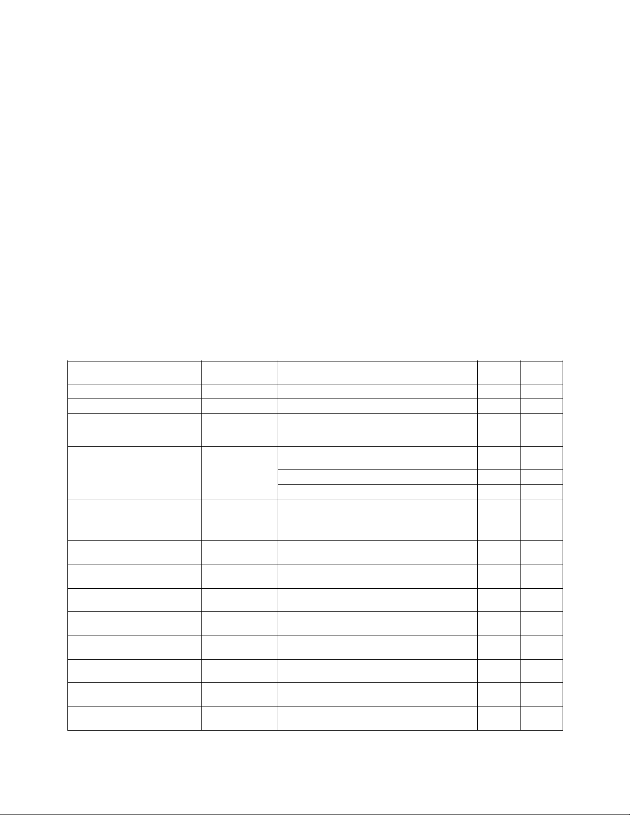
HSDL-1000 Reliability Test Results
Test Name Reference Test Conditions Tested Failed
Solder Heat (IR Profile) See absolute profile 60 0
Solder Heat Resistance 3 times thru IR Profile + 20 Temp. Cycles 60 0
Solder Rework Cycle Solder iron tip temp. 370°C/700°F170
Temperature Cycle 1010 -40°C to +100°C, Dwell = 15 Minutes
Power Temp. Cycle -40°C/+100°C, Dwell = 15 minutes, 60 0
Mechanical Shock 2002 2 Blows each X1, X2, Y1, Y2, Z1, Z2 10 0
Vibration Variable 2007 (4) 4 Minute Cycles, X, Y, Z 10 0
Frequency Condition A at 50 G’s Min., 20 to 2,000 Hz
Resistance to Solvents 2015 3 one minute immersion 20 0
High Temp. Operating TA= 70°C, If = 100 mAdc, VCC = 5 Vdc, 60 0
Life Time = 500 hours
Low Temp. Opearting Life TA = 0°C, If = 100 mAdc, VCC = 5 Vdc 60 0
Wet Operating Life TA = 35°C, R.H., = 85% If = 100 mAdc 60 0
ESD - Human Body Model 3015 RI = 1500 Ohms, C = 100 µF100
ESD - Machine Model EIAJ Rload = 0 Ohms, C = 200 µF100
MIL-STD-883 Units Total
Time per lead 1 second
# of rework cycles = 4
Transfer = 5 Minutes
20 Cycles 120 0
100 Cycles 120 0
Transfer = 5 Minutes, VCC = 5 Vdc,
If = 100 mAdc, LED On/Off = 1 Second
Total Cycles = 35
Condition B 1500 G’s, 0.5 msec Pulse
Brush after solvent
Time = 500 hours
VCC = 5 VCC, Time = 500 hours
Level = 4000 V
Level = 300 V
Note: At the time of this publication, Light Emitting Diodes (LEDs) that are contained in this product are regulated for eye safety in
Europe by the Commission for European Electrotechnical Standardization (CENELEC) EN60825-1. Please refer to Application Briefs
I-008, I-009, I-015 for more information.
4-42
 Loading...