

Page 1

September 1995
HS-82C55ARH
Radiation Hardened
CMOS Programmable Peripheral Interface
Features
• Radiation Hardened
- Total Dose >10
- Transient Upset <10
- Latch Up Free EPI-CMOS
• Low Power Consumption
- IDDSB = 20µA
• Pin Compatible with NMOS 8255A and the Intersil 82C55A
• High Speed, No “Wait State” Operation with 5MHz HS-80C86RH
• 24 Programmable I/O Pins
• Bus-Hold Circuitry on All I/O Ports Eliminates Pull-Up Resistors
• Direct Bit Set/Reset Capability
• Enhanced Control Word Read Capability
• Hardened Field, Self-Aligned, Junction Isolated CMOS Process
• Single 5V Supply
• 2.0mA Drive Capability on All I/O Port Outputs
• Military Temperature Range: -55
5
RAD (Si)
8
RAD (Si)/s
o
C to +125oC
Description
The Intersil HS-82C55ARH is a high performance, radiation hardened
CMOS version of the industry standard 8255A and is manufactured using a
hardened field, self-aligned silicongate CMOS process. It is a general
purpose programmable I/O device which may be used with many different
microprocessors. There are 24 I/O pins which are organized into two 8-bit
and two 4-bit ports. Each port may be programmed to function as either an
input or an output. Additionally, one of the 8-bit ports may be programmed
for bi-directional operation,and the two 4-bit ports can be programmed to
provide handshaking capabilities. The high performance, radiation
hardness, and industry standard configuration of the HS-82C55ARH make
it compatible with the HS-80C86RH radiation hardened microprocessor.
Static CMOS circuit design insures low operating power. Bus hold circuitry
eliminates the need for pull-up resistors. The Intersil hardened field CMOS
process results in performance equal to or greater than existing radiation
resistant products at a fraction of the power.
Pinout
40 LEAD CERAMIC DUAL-IN-LINE
METAL SEAL PACKAGE (SBDIP)
MIL-STD-1835 CDIP2-T40
TOP VIEW
1
PA3
PA2
PA1
PA0
RD
CS
GND
A1
A0
PC7
PC6
PC5
PC4
PC0
PC1
PC2
PC3
PB0
PB1
PB2
2
3
4
5
6
7
8
9
10
11
12
13
14
15
16
17
18
19
20
40
39
38
37
36
35
34
33
32
31
30
29
28
27
26
25
24
23
22
21
PA4
PA5
PA6
PA7
WR
RESET
D0
D1
D2
D3
D4
D5
D6
D7
VDD
PB7
PB6
PB5
PB4
PB3
Pin Description
PIN DESCRIPTION
D7 - D0 Data Bus (Bi-Directional
RESET Reset Input
CS Chip Select
RD Read Input
WR Write Input
Ordering Information
PART NUMBER TEMPERATURE PACKAGE
HS1-82C55ARH-Q -55oC to +125oC 40 Lead SBDIP
HS1-82C55ARH-8 -55oC to +125oC 40 Lead SBDIP
HS1-82C55ARH/Sample +25oC 40 Lead SBDIP
CAUTION: These devices are sensitive to electrostatic discharge; follow proper IC Handling Procedures.
http://www.intersil.com or 407-727-9207
| Copyright © Intersil Corporation 1999
970
A0 - A1 Port Address
PA7 - PA0 Port A (Bit)
PB& - PB0 Port B (Bit)
PC7 - PC0 Port C (Bit)
VDD +5 volts
GND 0 volts
Spec Number
File Number 3191.1
DB NA
518060
Page 2

HS-82C55ARH
Pin Description
PIN
SYMBOL
PA0-7 1-4, 37-40 I/O Port A: General purpose I/O Port. Data direction and mode is determined by the contents
PB0-7 18-25 I/O Port B: General purpose I/O port. See Port A.
PC0-3 14-17 I/O Port C (Lower): Combination I/O port and control port associated with Port B. See Port A.
PC4-7 10-13 I/O Port C (Upper): Combination I/O Port and control port associated with Port A. See Port A.
D0-7 27-34 I/O Bidirectional Data Bus: Three-State data bus enabled as an input when CS and WR are
VDD 26 I VDD: The +5V power supply pin. A 0.1µF capacitor between pins 26 and 7 is recommend-
GND 7 I Ground.
CS 6 I Chip Select: A “low” on this input pin enables the communication between the
RD 5 I Read: A “low” on this input pin enables the HS-82C55ARH to send the data or status
WR 36 I Write: A “low” on this input pin enables the CPU to write data or control words into the
A0 and A1 8, 9 I Port Select 0 and Port Select 1: These input signals, in conjunction with the RD and WR
Reset 35 I Reset: A “high” on this input clears the control register and all ports (A, B, C) are set to the
NUMBERS TYPE DESCRIPTION
of the Control Word.
low and as an output when CS and RD are low.
ed for decoupling.
HS-82C55ARH and the CPU.
information to the CPU on the data bus. In essence, it allows the CPU to “read from” the
HS-82C55ARH.
HS-82C55ARH.
inputs, control the selection of one of the three ports or the control word registers. They are
normally connected to the Least Significant Bits of the address bus (A0 and A1).
input mode. “Bus hold” devices internal to the HS-82C55ARH will hold the I/O port inputs
to a logic “1” state with a maximum hold current of 400µA.
Functional Diagram
POWER
SUPPLIES
BIDIRECTIONAL
DATA BUS
D7 - D0
RD
WR
A1
A0
RESET
READ/WRITE
DATA
BUS
BUFFER
CONTROL
LOGIC
+5V
GND
GROUP A
CONTROL
8-BIT INTERNAL
GROUP B
CONTROL
DATA BUS
GROUP A
PORT A
(8)
GROUP A
PORT C
UPPER (4)
GROUP B
PORT C
LOWER (4)
GROUP B
PORT B
(8)
I/O
PA7 - PA0
I/O
PC7 - PC4
I/O
PC3 - PC0
I/O
PB7 - PB0
CS
Spec Number 518060
971
Page 3
Specifications HS-82C55ARH
Absolute Maximum Ratings Reliability Information
Supply Voltage . . . . . . . . . . . . . . . . . . . . . . . . . . . . . . . . . . . . .+7.0V
Input, Output or I/O Voltage . . . . . . . . . . . . .VSS-0.3V to VDD+0.3V
Storage Temperature Range . . . . . . . . . . . . . . . . . -65oC to +150oC
Junction Temperature. . . . . . . . . . . . . . . . . . . . . . . . . . . . . . +175oC
Lead Temperature (Soldering 10s). . . . . . . . . . . . . . . . . . . . +300oC
ESD Classification . . . . . . . . . . . . . . . . . . . . . . . . . . . . . . . . Class 1
CAUTION: Stresses above those listed in “Absolute Maximum Ratings” may cause permanent damage to the device. This is a stress only rating and operation
of the device at these or any other conditions above those indicated in the operational sections of this specification is not implied.
Operating Conditions
Operating Voltage Range. . . . . . . . . . . . . . . . . . . . . +4.5V to +5.5V
Operating Temperature Range. . . . . . . . . . . . . . . . -55oC to +125oC
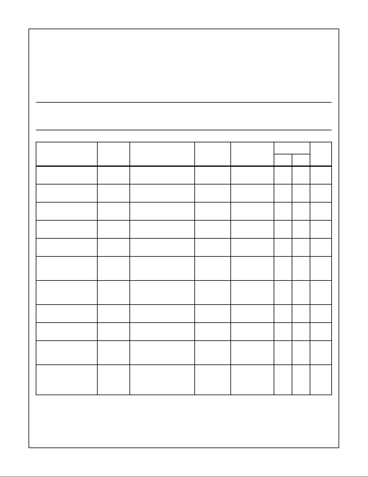
TABLE 1. DC ELECTRICAL PERFORMANCE CHARACTERISTICS
PARAMETER SYMBOL CONDITIONS
Thermal Resistance θ
SBDIP Package. . . . . . . . . . . . . . . . . . . . 40oC/W 6oC/W
Maximum Package Power Dissipation at +125oC Ambient
SBDIP Package. . . . . . . . . . . . . . . . . . . . . . . . . . . . . . . . . .1.25W
If device power exceeds package dissipation capability, provide heat
sinking or derate linearly at the following rate:
SBDIP Package. . . . . . . . . . . . . . . . . . . . . . . . . . . . . . .25.0mW/C
Input Low Voltage . . . . . . . . . . . . . . . . . . . . . . . . . . . . . .0V to +0.8V
Input High Voltage. . . . . . . . . . . . . . . . . . . . . . . . VDD -1.5V to VDD
GROUP A
SUBGROUP TEMPERATURE
JA
LIMITS
θ
JC
UNITSMIN MAX
TTL Output High Voltage VOH1 VDD = 4.5V, IO = -2.5mA,
VIN = 0V, 4.5V
CMOS Output High Voltage
Output Low Voltage VOL VDD = 4.5V, IO = 2.5mA,
Input Leakage Current IIL or IIH VDD = 5.5V, VIN = 0V, 5.5V 1, 2, 3 -55oC, +25oC,
Output Leakage Current IOZL or
Input Current Bus Hold
High
Input Current Bus Hold
Low
Standby Power Supply
Current
Darlington Drive Voltage VDAR VDD = 4.5V, IO = -2.0mA,
Functional Tests FT VDD = 4.5V and 5.5V,
VOH2 VDD = 4.5V, IO = -100µA,
VIN = 0V, 4.5V
VIN = 0V, 4.5V
VDD = 5.5V, VIN = 0V, 5.5V 1, 2, 3 -55oC, +25oC,
IOZH
IBHH VDD = 4.5V or 5.5V,
VIN = 3.0V (See Note 1)
Ports A, B, C
IBHL VDD = 4.5V or 5.5V,
VIN = 1.0V (See Note 2)
Port A
IDDSB VDD = 5.5V, IO = 0mA,
VIN =GND or VDD
VIN = GND or VDD
VIN = GND or VDD,
f = 1MHz
1, 2, 3 -55oC, +25oC,
+125oC
1, 2, 3 -55oC, +25oC,
+125oC
1, 2, 3 -55oC, +25oC,
+125oC
+125oC
+125oC
1, 2, 3 -55oC, +25oC,
+125oC
1, 2, 3 -55oC, +25oC,
+125oC
1, 2, 3 -55oC, +25oC,
+125oC
1, 2, 3 -55oC, +25oC,
+125oC
7, 8A, 8B -55oC, +25oC,
+125oC
3.0 - V
VDD-
0.4
- 0.4 V
-1.0 1.0 µA
-10 10 µA
-800 -60 µA
60 800 µA
-20µA
3.9 - V
-- -
-V
Noise Immunity Functional
Test (Note 4)
NOTES:
1. IBHH should be measured after raising VIN and then lowering to 3.0V.
2. IBHL should be measured after lowering VIN to VSS and then raising to 0.8V.
3. No internal current limiting exists on the Port Outputs. A resistor must be added externally to limit the current.
4. For VIH (VDD = 5.5V) and VIL (VDD = 4.5V) each of the following groups is tested separately with all other inputs using VIH = 2.6V,
VIL = 0.4V: PA, PB, PC, Control Pins (Pins 5, 6, 8, 9, 35, 36).
FN VDD = 5.5V, VIN = GND or
VDD - 1.5V and
VDD = 4.5V, VIN = 0.8V or
VDD
7, 8A, 8B -55oC, +25oC,
+125oC
-- -
Spec Number 518060
972
Page 4
Specifications HS-82C55ARH
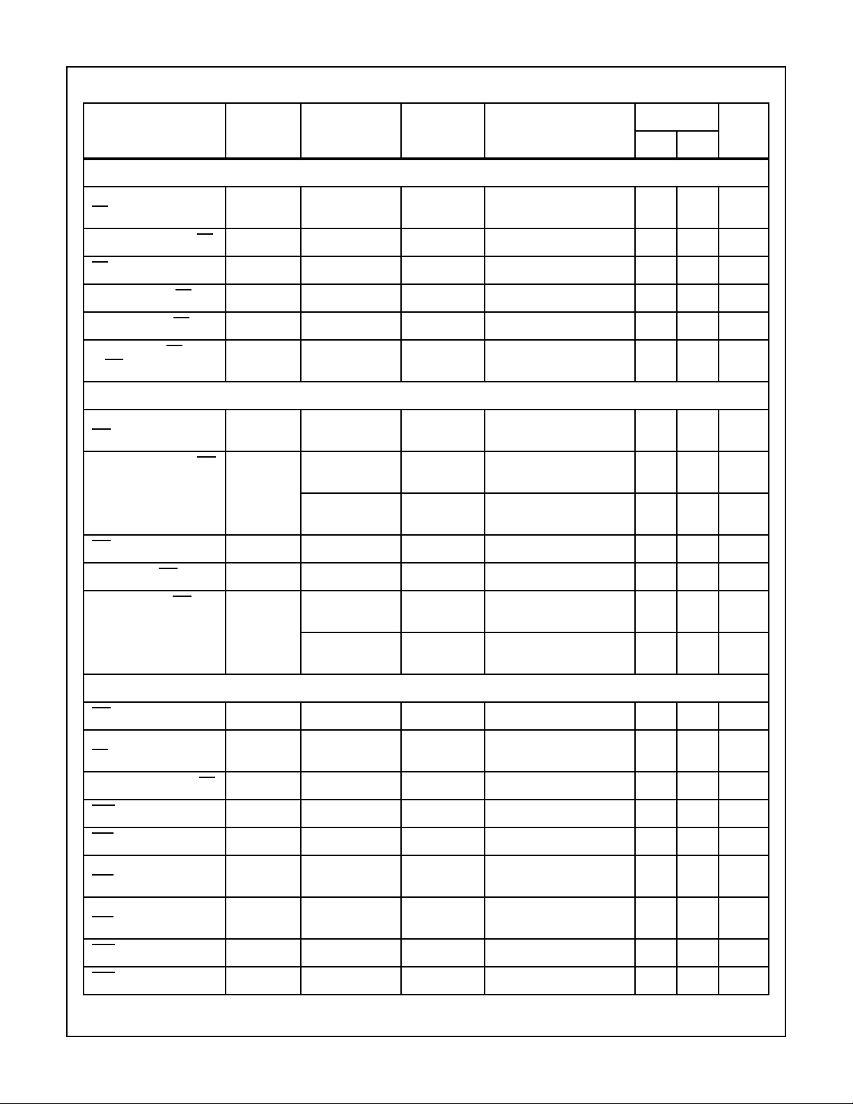
TABLE 2. AC ELECTRICAL PERFORMANCE CHARACTERISTICS TA = -55oC to +125oC
PARAMETER SYMBOL CONDITIONS
READ
SUB-
GROUPS TEMPERATURE
LIMITS
UNITSMIN MAX
Address Stable Before
RD
Address Stable After RD TRHAX VDD = 4.5, 5.5V 9, 10, 11 -55oC, +25oC, +125oC0-ns
RD Pulse Width TRLRH VDD = 4.5, 5.5V 9, 10, 11 -55oC, +25oC, +125oC 250 - ns
Data Valid From RD TRLDV VDD = 4.5, 5.5V 9, 10, 11 -55oC, +25oC, +125oC - 200 ns
Data Float After RD TRHDX VDD = 4.5, 5.5V 9, 10, 11 -55oC, +25oC, +125oC10- ns
Time Between RDs and/
or WRs
WRITE
Address Stable Before
WR
Address Stable After WR TWHAX VDD = 4.5, 5.5V,
WR Pulse Width TWLWH VDD = 4.5, 5.5V 9, 10, 11 -55oC, +25oC, +125oC 100 - ns
Data Valid to WR High TDVWH VDD = 4.5, 5.5V 9, 10, 11 -55oC, +25oC, +125oC 100 - ns
Data Valid After WR High TWHDX VDD = 4.5, 5.5V,
TAVRL VDD = 4.5, 5.5V 9, 10, 11 -55oC, +25oC, +125oC0-ns
TRWHRWL VDD = 4.5, 5.5V 9, 10, 11 -55oC, +25oC, +125oC 300 - ns
TAVWL VDD = 4.5, 5.5V 9, 10, 11 -55oC, +25oC, +125oC0-ns
9, 10, 11 -55oC, +25oC, +125oC20- ns
Ports A and B
VDD = 4.5, 5.5V,
Port C
Ports A and B
9, 10, 11 -55oC, +25oC, +125oC 100 - ns
9, 10, 11 -55oC, +25oC, +125oC30- ns
VDD = 4.5, 5.5V,
Port C
OTHER TIMINGS
WR = 1 to Output TWHPV VDD = 4.5, 5.5V 9, 10, 11 -55oC, +25oC, +125oC - 350 ns
Peripheral Data Before
RD
Peripheral Data After RD TRHPX VDD = 4.5, 5.5V 9, 10, 11 -55oC, +25oC, +125oC0-ns
ACK Pulse Width TKLKH VDD = 4.5, 5.5V 9, 10, 11 -55oC, +25oC, +125oC 200 - ns
STB Pulse Width TSLSH VDD = 4.5, 5.5V 9, 10, 11 -55oC, +25oC, +125oC 100 - ns
Peripheral Data Before
STB High
Peripheral Data After
STB High
ACK = 0 to Output TKLPV VDD = 4.5, 5.5V 9, 10, 11 -55oC, +25oC, +125oC - 175 ns
ACK = 1 to output Float TKHPZ VDD = 4.5, 5.5V 9, 10, 11 -55oC, +25oC, +125oC10- ns
TPVRL VDD = 4.5, 5.5V 9, 10, 11 -55oC, +25oC, +125oC0-ns
TPVSH VDD = 4.5, 5.5V 9, 10, 11 -55oC, +25oC, +125oC20- ns
TSHPX VDD = 4.5, 5.5V 9, 10, 11 -55oC, +25oC, +125oC50- ns
9, 10, 11 -55oC, +25oC, +125oC 100 -
973
Spec Number 518060
Page 5

Specifications HS-82C55ARH
TABLE 2. AC ELECTRICAL PERFORMANCE CHARACTERISTICS TA = -55oC to +125oC (Continued)
LIMITS
SUB-
PARAMETER SYMBOL CONDITIONS
WR = 1 to OBF = 0 TWHOL VDD = 4.5, 5.5V 9, 10, 11 -55oC, +25oC, +125oC - 150 ns
ACK = 0 to OBF = 1 TKLOH VDD = 4.5, 5.5V 9, 10, 11 -55oC, +25oC, +125oC - 150 ns
STB = 0 to IBF = 1 TSLIH VDD = 4.5, 5.5V 9, 10, 11 -55oC, +25oC, +125oC - 150 ns
RD = 1 to IBF = 0 TRHIL VDD = 4.5, 5.5V 9, 10, 11 -55oC, +25oC, +125oC - 150 ns
RD = 0 to INTR = 1 TRLNL VDD = 4.5, 5.5V 9, 10, 11 -55oC, +25oC, +125oC - 200 ns
STB = 1 t INTR = 1 TSHNH VDD = 4.5, 5.5V 9, 10, 11 -55oC, +25oC, +125oC - 150 ns
ACK = 1 to INTR = 1 TKHNH VDD = 4.5, 5.5V 9, 10, 11 -55oC, +25oC, +125oC - 150 ns
WR = 0 to INTR = 0 TWLNL VDD = 4.5, 5.5V 9, 10, 11 -55oC, +25oC, +125oC - 200 ns
GROUPS TEMPERATURE
UNITSMIN MAX
RESET Pulse Width TRSHRSL VDD = 4.5, 5.5V
(Note 2)
NOTES:
1. AC’s tested at worst case VDD, guaranteed over full operating range.
2. Period of initial RESET pulse after power-on must be at least 50µs. Subsequenct RESET pulses may be 500ns minimum.
TABLE 3. ELECTRICAL PERFORMANCE CHARACTERISTICS
PARAMETER SYMBOL CONDITIONS TEMPERATURE
Input Capacitance CIN VDD = Open, f = 1MHz, All
measurements referenced to
device ground
I/O Capacitance CI/O VDD = Open, f = 1MHz, All
measurements referenced to
device ground
Data Float After RD TRHDX VDD = 4.5V and 5.5V -55oC < TA < +125oC - 75 ns
ACK = 1 to Output Float TKHPZ VDD = 4.5V and 5.5V -55oC < TA < +125oC - 250 ns
NOTE: The parameters listed in Table 3 are controlled via design or process parameters and are not directly tested. These parameters are
characterized upon initial design release and upon design changes which would affect these characteristics
9, 10, 11 -55oC, +25oC, +125oC 500 - ns
LIMITS
UNITSMIN MAX
TA = +25oC - 10 pF
TA = +25oC - 20 pF
TALBE 4. POST 100K RAD ELECTRICAL PERFORMANCE CHARACTERISTICS
See +25oC limits in Table 1 and Table 2 for Post RAD limits (Subgroups 1, 7, 9)
974
Spec Number 518060
Page 6
Specifications HS-82C55ARH
TABLE 5. BURN-IN DELTA PARAMETERS (+25oC)
PARAMETER SYMBOL DELTA LIMITS
Static Current IDDSB ±10µA
Input Leakage Current IIL, IIH ±200nA
Output Leakage Current IOZL, IOZH ±2µA
Low Level Output Voltage VOL ±80mV
TTL Output High Voltage VOH1 ±600mV
CMOS Output High Voltage VOH2 ±150mV
TABLE 6. APPLICABLE SUBGROUPS
GROUP A SUBGROUPS
CONFORMANCE
GROUP
Initial Test 100% 5004 1, 7, 9 1 (Note 2) 1, 7, 9
Interim Test 100% 5004 1, 7, 9,∆ 1, ∆ (Note 2) 1, 7, 9
PDA 100% 5004 1, 7, ∆ - 1, 7
Final Test 100% 5004 2, 3, 8A, 8B, 10, 11 - 2, 3, 8A, 8B, 10, 11
Group A (Note 1) Sample 5005 1, 2, 3, 7, 8A, 8B, 9, 10, 11 - 1, 2, 3, 7, 8A, 8B, 9,
Subgroup B5 Sample 5005 1, 2, 3, 7, 8A, 8B, 9, 10, 11, ∆ 1, 2, 3, ∆ (Note 2) N/A
Subgroup B6 Sample 5005 1, 7, 9 - N/A
Group C Sample 5005 N/A N/A 1, 2, 3, 7, 8A, 8B, 9,
Group D Sample 5005 1, 7, 9 - 1, 7, 9
Group E, Subgroup 2 Sample 5005 1, 7, 9 - 1, 7, 9
NOTES:
1. Alternate Group A testing in accordance with MIL-STD-883 method 5005 may be exercised.
2. Table 5 parameters only
MIL-STD-883
METHOD
TESTED FOR -Q
RECORDED
FOR -Q TESTED FOR -8
10, 11
10, 11
RECORDED
FOR -8
975
Spec Number 518060
Page 7

HS-82C55ARH
Intersil Space Level Product Flow -Q
Wafer Lot Acceptance (All Lots) Method 5007
(Includes SEM)
GAMMA Radiation Verification (Each Wafer) Method 1019,
2 Samples/Wafer, 0 Rejects
100% Die Attach
100% Nondestructive Bond Pull, Method 2023
Sample - Wire Bond Pull Monitor, Method 2011
Sample - Die Shear Monitor, Method 2019 or 2027
100% Internal Visual Inspection, Method 2010, Condition A
CSI and/or GSI PreCap (Note 6)
100% Temperature Cycle, Method 1010, Condition C,
10 Cycles
100% Constant Acceleration, Method 2001, Condition per
Method 5004
100% PIND, Method 2020, Condition A
100% External Visual
100% Serialization
100% Initial Electrical Test (T0)
100% Static Burn-In 1, Condition A or B, 72 Hours Min,
NOTES:
1. Failures from subgroup 1, 7 and deltas are used for calculating PDA. The maximum allowable PDA = 5% with no more than 3% of the
2. Radiographic (X-Ray) inspection may be performed at any point after serialization as allowed by Method 5004.
3. Alternate Group A testing may be performed as allowed by MIL-STD-883, Method 5005.
4. Group B and D inspections are optional and will not be performed unless required by the P.O. When required, the P.O. should include
5. Group D Generic Data, as defined by MIL-I-38535, is optional and will not be supplied unless required by the P.O. When required, the
6. CSI and/or GSI inspections are optional and will not be performed unless required by theP.O. When required, the P.O. should include
7. Data Package Contents:
tity).
o
C Min, Method 1015
+125
failures from subgroup 7.
separate line items for Group B Test, Group B Samples, Group D Test and Group D Samples.
P.O. should include a separate line item for Group D Generic Data. Generic data is not guaranteed to be available and is therefore not
available in all cases.
separate line items for CSI PreCap inspection, CSI final inspection, GSI PreCap inspection, and/or GSI final inspection.
• Cover Sheet (Intersil Name and/or Logo, P.O. Number, Customer Part Number, Lot Date Code, Intersil Part Number, Lot Number, Quan-
• Wafer Lot Acceptance Report (Method 5007). Includes reproductions of SEM photos with percent of step coverage.
• GAMMA Radiation Report. Contains Cover page, disposition, Rad Dose, Lot Number, T est Package used, Specification Numbers, Test
equipment, etc. Radiation Read and Record data on file at Intersil.
• X-Ray report and film. Includes penetrometer measurements.
• Screening, Electrical, and Group A attributes (Screening attributes begin after package seal).
• Lot Serial Number Sheet (Good units serial number and lot number).
• Variables Data (All Delta operations). Data is identified by serial number. Data header includes lot number and date of test.
• Group B and D attributes and/or Generic data is included when required by the P.O.
• The Certificate of Conformance is a part of the shipping invoice and is not part of the Data Book. The Certificate of Conformance is signed
by an authorized Quality Representative.
100% Interim Electrical Test 1 (T1)
100% Delta Calculation (T0-T1)
100% PDA 1, Method 5004 (Note 1)
100% Dynamic Burn-In, Condition D, 240 Hours, +125
Equivalent, Method 1015
100% Interim Electrical Test 2(T2)
100% Delta Calculation (T0-T2)
100% PDA 2, Method 5004 (Note 1)
100% Final Electrical Test
100% Fine/Gross Leak, Method 1014
100% Radiographic (X-Ray), Method 2012 (Note 2)
100% External Visual, Method 2009
Sample - Group A, Method 5005 (Note 3)
Sample - Group B, Method 5005 (Note 4)
Sample - Group D, Method 5005 (Notes 4 and 5)
100% Data Package Generation (Note 7)
CSI and/or GSI Final (Note 6)
o
C or
976
Spec Number 518060
Page 8

HS-82C55ARH
Intersil Space Level Product Flow -8
GAMMA Radiation Verification (Each Wafer) Method 1019,
2 Samples/Wafer, 0 Rejects
100% Die Attach
Periodic- Wire Bond Pull Monitor, Method 2011
Periodic- Die Shear Monitor, Method 2019 or 2027
100% Internal Visual Inspection, Method 2010, Condition B
CSI an/or GSI PreCap (Note 5)
100% Temperature Cycle, Method 1010, Condition C,
10 Cycles
100% Constant Acceleration, Method 2001, Condition per
Method 5004
100% External Visual
100% Initial Electrical Test
NOTES:
1. Failures from subgroup 1, 7 are used for calculating PDA. The maximum allowable PDA = 5%.
2. Alternate Group A testing may be performed as allowed by MIL-STD-883, Method 5005.
3. Group B, C and D inspections are optional and will not be performed unless required by the P.O. When required, the P.O. should include
separate line items for Group B Test, Group C Test, Group C Samples, Group D Test and Group D Samples.
4. Group C and/or Group D Generic Data, as defined by MIL-I-38535, is optional and will not be supplied unless required by the P.O. When
required, the P.O. should include a separate line item for Group C Generic Data and/or Group D Generic Data. Generic data is not guaranteed to be available and is therefore not available in all cases.
5. CSI and/or GSI inspections are optional and will not be performed unless required by theP.O. When required, the P.O. should include
separate line items for CSI PreCap inspection, CSI final inspection, GSI PreCap inspection, and/or GSI final inspection.
6. Data Package Contents:
• Cover Sheet (Intersil Name and/or Logo, P.O. Number, Customer Part Number, Lot Date Code, Intersil Part Number, Lot Number, Quan-
tity).
• GAMMA Radiation Report. Contains Cover page, disposition, Rad Dose, Lot Number, T est Package used, Specification Numbers, Test
equipment, etc. Radiation Read and Record data on file at Intersil.
• Screening, Electrical, and Group A attributes (Screening attributes begin after package seal).
• Group B, C and D attributes and/or Generic data is included when required by the P.O.
• The Certificate of Conformance is a part of the shipping invoice and is not part of the Data Book. The Certificate of Conformance is signed
by an authorized Quality Representative.
100% Dynamic Burn-In, Condition D, 160 Hours, +125
Equivalent, Method 1015
100% Interim Electrical Test
100% PDA, Method 5004 (Note 1)
100% Final Electrical Test
100% Fine/Gross Leak, Method 1014
100% External Visual, Method 2009
Sample - Group A, Method 5005 (Note 2)
Sample - Group B, Method 5005 (Note 3)
Sample - Group C, Method 5005 (Notes 3 and 4)
Sample - Group D, Method 5005 (Notes 3 and 4)
100% Data Package Generation (Note 6)
CSI and/or GSI Final (Note 5)
o
C or
AC Test Circuit
V1
R1
FROM OUTPUT
UNDER TEST
R2
* Includes stray and jig capacitance
TEST CONDITIONS DEFINITION TABLE
V1 R1 R2 C1
1.7V 523Ω Open 150pF
C1*
TEST
POINT
AC Testing Input, Output Waveforms
INPUT
2.8V
0.4V
NOTE: AC Testing: All parameters tested as per test circuits. Input
rise and fall times are driven at 1V/ns.
977
1.5V 1.5V
Spec Number 518060
Page 9

Waveforms
HS-82C55ARH
RD
INPUT
CS, A1, A0
D7 - D0
STB
IBF
INTR
RD
INPUT FROM
PERIPHERAL
TRLRH
TPVRL TRHPX
TAVRL TRHAX
TRLDV TRHDZ
FIGURE 1. MODE 0 (BASIC INPUT)
TSLSH
TSLIH
TSHNH
TPVSH
TRLNL
TRHIL
TSHPX
WR
D7 - D0
CS, A1, A0
OUTPUT
WR
OBF
INTR
ACK
OUTPUT
TAVWL
FIGURE 2. MODE 0 (BASIC OUTPUT)
TWLNL
TWHPV
TWLWH
TDVWH
TWHPV
TWHOL
TKLOH
TKLKH
TKHNH
FIGURE 3. MODE 1 (STROBED INPUT) FIGURE 4. MODE 1 (STROBED OUTPUT)
TWHDX
TWHAX
DATA FROM CPU
TO HS-82C55ARH
WR
OBF
INTR
ACK
STB
IBF
PERIPHERAL
BUS
RD
DATA FROM PERI-
PHERAL TO
HS-82C55ARH
TWHOL
TSLIH
TKLOH
TSLSH
TKLPV
TPVSH
TSHPX
DATA FROM
HS-82C55ARH
TO PERIPHERAL
TKLKH
TKHPX
TRHIL
DATA FROM
HS-82C55ARH
TO CPU
FIGURE 5. MODE 2 (BIDIRECTIONAL)
NOTE: Any sequence where WR occurs before ACK andSTB occurs
before RD is permissible.
A0 - A1, CS
DATA BUS
A0 - A1, CS
RD
DATA BUS
TAVWL TWHAX
WR
TWLWH
FIGURE 6. WRITE TIMING
TAVRL TRHAX
TAVRL
HIGH IMPEDANCE VALID
FIGURE 7. READ TIMING
TDVWH
TRLRH
TWHDX
TRHDX
HIGH IMPEDANCE
978
Spec Number 518060
Page 10

Burn-In Circuits
PROGRAMMABLE PERIPHERAL INTERFACE
HS-82C55ARH
PROGRAMMABLE PERIPHERAL INTERFACE
VDD
1
2
3
4
5
6
7
8
9
10
11
12
13
14
15
16
17
18
19
20
40
39
38
37
36
35
34
33
32
31
30
29
28
27
26
25
24
23
22
21
F5
F0
F0
F4
F0
F2
F1
1
2
3
4
5
6
7
8
9
10
11
12
13
14
15
16
17
18
19
20
40
39
38
37
36
35
34
33
32
31
30
29
28
27
26
25
24
23
22
21
F0
F4
F6
F5
F7
F3
VDD
NOTES:
1. VDD = 6.0V ± 0. 5%
2. IDD <500µA
3. TA Min = +125oC
STATIC CONFIGURATION
DYNAMIC CONFIGURATION
NOTES:
1. VDD = 6.0V ± 5% for Burn-In
2. VDD = 5.0V ± 5% for Life Test
3. All resistors are 10KΩ± 5%
4. -0.3V ≤ VIL ≤ 0.8V
5. VDD - 1.0V ≤ VIH ≤ VDD
6. IDD < 5mA
7. F0 = 10KHz, 50% Duty cycle
8. F1 = F0/2; F2 = F1/2; F3 = F2/2; F4 = F3/2 . . . F7 = F6/2
9. TA Min = +125oC
979
Spec Number 518060
Page 11

Irradiation Circuit
HS-82C55ARH
CMOS PROGRAMMABLE PERIPHERAL INTERFACE
NOTE:
1. VDD = 5.5V
1
2
3
4
5
6
7
+5.5V +5.5V
8
9
10
11
12
13
14
15
16
17
18
19
20
40
39
38
37
36
35
34
33
32
31
30
29
28
27
26
25
24
23
22
21
980
Spec Number 518060
Page 12

HS-82C55ARH
Functional Description
The HS-82C55ARH is a programmable peripheral interface
designed to allow microcomputer systems to control and
interface with all types of peripheral devices.It has the
ability to generate and respond to all asynchronous handshaking signals necessary to transfer data to and from
peripheral devices, and it can also interrupt the processor
when a peripheral needs servicing. These capabilities allow
the HS-82C55ARH to be used in an unlimited number of
applications including EXTERNAL SYSTEM CONTROL,
ASYNCHRONOUS DATA TRANSFER, and SYSTEMS
MONITORING.
Data Bus Buffer
This tri-state bidirectional 8-bit buffer is used to interface the
HS-82C55ARH to the system data bus (see Figure 8). Data
is transmitted or received by the buffer upon execution of
input or output instructions by the CPU. Control words and
status information are also transferred through the data bus
buffer.
POWER
SUPPLIES
BIDIRECTIONAL
DATA BUS
D7D0
RD
WR
A1
A0
RESET
CS
GND
DATA
BUS
BUFFER
READ/
WRITE
CONTROL
LOGIC
+5V
GROUP
A
CONTROL
8-BIT INTERNAL
DATA BUS
GROUP
B
CONTROL
GROUP
A PORT
A (8)
GROUP
A PORT
C UPPER
(4)
GROUP
B PORT
C LOWER
(4)
GROUP
B PORT
B (8)
FIGURE 8. BLOCK DIAGRAM DATA BUS BUFFER, READ/WRITE,
GROUP A AND B CONTROL LOGIC FUNCTIONS
I/O
PA 7PA0
I/O
PC 7PC4
I/O
PC3PC0
I/O
PB 7PB0
Ports A, B, C
The HS-82C55ARH contains three 8-bit ports (A, B and C).
All can be configured to a wide variety of functional
characteristics by the system software but each has its own
special features or “personality” to further enhance the
power and flexibility of the HS-82C55ARH.
Port A One 8-bit data output latch/buffer and one 8-bit data
input latch. Both “pull-up” and “pull-down” bus hold
devices are present on Port A. See Figure 9A.
Port B One 8-bit data input/output latch/buffer and one 8-
bit data input buffer. See Figure 9B.
Port C One 8-bit data output latch/buffer and one 8-bit data
input buffer (no latch for input). This port can be
divided into two 4-bit ports under the mode control.
Each 4-bit port contains a 4-bit latch and can be used
for the control signal outputs and status signal inputs
in conjunction with Ports A and B. See Figure 9B.
(A)
RD
CONTROL
VDD
P
EXTERNAL
PORT A PIN
MASTER
RESET
INTERNAL
DATA IN
INTERNAL
DATA OUT
MASTER
RESET
WR
SIGNAL
Read/Write and Control Logic
The function of this block is to manage all of the internal and
external transfer of both Data and Control or Status words. It
accepts inputs from the CPU Address and Control busses
and in turn, issues commands to both of the Control Groups.
Group A and Group B Controls
The functional configuration of each port is programmed by
the systems software. In essence, the CPU writes a control
word to the HS-82C55ARH. The control word contains information such as “mode”, “bit set”, “bit reset”, etc., that initializes the functional configuration of the HS-82C55ARH.
Each of the Control blocks (Group A and Group B) accepts
“commands” from the Read/Write Control Logic, receives
“control words” from the internal data bus and issues the
proper commands to its associated ports.
Control Group - Port A and Port C upper (C7 - C4)
Control Group - Port B and Port C lower (C3 - C0).
INTERNAL
DATA IN
INTERNAL
DATA OUT
WR
SIGNAL
EXTERNAL
PORT B, C
PIN
(B)
FIGURE 9. I/O PORT CONFIGURATION
Operational Description
Control Word
The data direction and mode of Ports A, B and C are
determined by the contents of the Control Word. See Figure
11. The Control W ord can be both written and read as shown
in Table 1 and 2. During write operations, the function of the
Control Word being written is determined by data bit D7. If
D7 is low, the data on D0 - D3 will set or reset one of the bits
of Port C. See Figure 12. During read Operations, the
Spec Number 518060
981
Page 13

HS-82C55ARH
Control Word will always be in the format illustrated in Figure
11 with Bit D7 high to indicate Control Word Mode Information.
ADDRESS BUS
CONTROL BUS
DATA BUS
RD, WR D7 - D0 A0 - A1
MODE 0
MODE 1
MODE 2
BCA
8 4 84
I/O I/O I/O I/O
PB7 - PB0 PC3 - PC0 PC7 - PC4 PA7 - PA0
BCA
8 8
I/O I/O
PB7 - PB0 PA7 - PA0
PB7 - PB0 PA7 - PA0
CONTROL
OR I/O
BCA
8 8
I/O
I/O
CONTROL
OR I/O
CONTROL
FIGURE 10. BASIC MODE DEFINITIONS & BUS INTERFACE
TABLE 1.
INPUT OPERATION
A1 A0 RD WR CS
00010Port A - Data Bus
01010Port B - Data Bus
10010Port C - Data Bus
11010Control Word - Data Bus
TABLE 2.
OUTPUT OPERATION
A1 A0 RD WR CS
00100Data Bus - Port A
01100Data Bus - Port B
10100Data Bus - Port C
11100Data Bus - Control Word
CS
BIDIRECTIONAL
(READ)
(WRITE)
TABLE 3.
A1 A0 RD WR CS DISABLE FUNCTION
XXXX1Data Bus - 3-State
X X 1 1 0 Data Bus - 3-State
CONTROL WORD
D7 D6 D5 D4 D3 D2 D1 D0
GROUP B
PORT C (LOWER)
1 = INPUT
0 = OUTPUT
PORT B
1 = INPUT
0 = OUTPUT
MODE SELECTION
0 = MODE 0
1 = MODE 1
GROUP A
PORT C (UPPER)
1 = INPUT
0 = OUTPUT
PORT A
1 = INPUT
0 = OUTPUT
MODE SELECTION
00 = MODE 0
01 = MODE 1
1X = MODE 2
MODE SET FLAG
1 = ACTIVE
FIGURE 11. MODE SET CONTROL WORD FORMAT
Mode Selection
There are three basic modes of operation that can be
selected by the system software:
Mode 0 - Basic Input/Output
Mode 1 - Strobed Input/Output
Mode 2 - Bidirectional Bus
When the RESET input goes “high”, all ports will be set to
the input mode with all 24 port lines held at the logic “one”
level by internal bus hold devices. After reset, the HS82C55ARH can remain in the input mode with no additional
initialization required. This eliminates the need for pullup or
pulldown resistors in all CMOS designs. During the
execution of the system program, any of the other modes
may be selected using a single output instruction. This
allows a single HS-82C55ARH to service a variety of
peripheral devices with a simple software maintenance
routine.
The modes for Port A and Port B can be separately defined
while Port C is divided into two portions as required by the
Port A and Port B definitions. All of the output registers,
including the status register, will be reset whenever the
mode is changed. Modes may be combined so that their
functional definition can be “tailored” to almost any I/O structure. For instance: Group B can be programmed in Mode 0
to monitor simple switch closings or display computational
results, Group A could be programmed in Mode 1 to monitor
a keyboard or tape recorder on an interrupt-driven basis.
982
Spec Number 518060
Page 14

HS-82C55ARH
The mode definitions and possible mode combinations may
seem confusing at first but after a cursory review of the
complete device operation a simple, logical I/O approach will
surface. The design of the HS-82C55ARH has taken into
account things such as efficient PC board layout, control
signal definition vs PC layout and complete functional
flexibility to support almost any peripheral device with no
external logic. Such design represents the maximum use of
the available pins.
CONTROL WORD
D7 D6 D5 D4 D3 D2 D1 D0
BIT SET/RESET
XXX
DON’T
CARE
FIGURE 12. BIT SET/RESET CONTROL WORD FORMAT
1 = SET
0 = RESET
BIT SELECT
0
1
2
3
4
5
6
0
1
0
1
0
1
0
0
0
1
1
0
0
1
0
0
0
0
1
1
1
BIT SET/RESET FLAG
0 = ACTIVE
7
1
B0
1
B1
1
B2
Single Bit/Set/Reset Feature
Any of the eight bits of Port C can be Set or Reset using a
single OUTput instruction. See Figure 12. This feature
reduces software requirements in control-based
applications.
Interrupt Control Functions
When the HS-82C55ARH is programmed to operate in
Mode 1 or Mode 2, control signals are provided that can be
used as interrupt request inputs to the CPU. The interrupt
request signals, generated from Port C, can be inhibited or
enable by setting or resetting the associated INTE flip-flop,
using the Bit Set/Reset function of Port C.
This function allows the programmer to enable or disable a
CPU interrupt by a specific I/O device without affecting any
other device in the interrupt structure.
INTE Flip-Flop Definition:
(BIT-SET) - INTE is SET - Interrupt enable.
(BIT-RESET) - INTE is RESET - Interrupt disable.
NOTE: All mask flip-flops are automatically reset during
mode selection and device Reset.
Operating Modes
Mode 0 (Basic Input/Output)
This functional configuration provides simple input and output operations for each of the three ports. No handshaking it
required, data is simply written to or read from a specific
port.
Mode 0 Basic Functional Definitions:
• Two 8-bit ports and two 4-bit ports
• Any port can be input or output
• Outputs are latched
• Inputs are not latched
• 16 different Input/Output configurations possible
RD
INPUT
CS, A1, A0
D7 - D0
WR
D7 - D0
CS, A1, A0
OUTPUT
TRLRH
TPVRL TRHPX
TAVRL TRHAX
TRLDV TRHDX
FIGURE 13. MODE 0 (BASIC INPUT)
TWLWH
TDVWH
TAVWL
FIGURE 14. MODE 0 (BASIC OUTPUT)
TWHDX
TWHAX
TWHPV
983
Spec Number 518060
Page 15

Mode 0 Port Definition
HS-82C55ARH
A B GROUP A
D4 D3 D1 D0 PORT A PORT C (UPPER) PORT B PORT C (LOWER)
NO.
GROUP B
0000Output Output 0 Output Output
0001Output Output 1 Output Input
0010Output Output 2 Input Output
0011Output Output 3 Input Input
0100Output Input 4 Output Output
0101Output Input 5 Output Input
0110Output Input 6 Input Output
0111Output Input 7 Input Input
1000 Input Output 8 Output Output
1001 Input Output 9 Output Input
1010 Input Output 10 Input Output
1011 Input Output 11 Input Input
1100 Input Input 12 Output Output
1101 Input Input 13 Output Input
1110 Input Input 14 Input Output
1111 Input Input 15 Input Input
Mode 0 Configurations
CONTROL WORD #0 CONTROL WORD #1
D7 D6 D5 D4 D3 D2 D1 D0
10000000
A
D7 - D0
CONTROL WORD #2 CONTROL WORD #3
D7 D6 D5 D4 D3 D2 D1 D0
10000010
D7 - D0
C
B
A
C
B
8
4
4
8
8
4
4
8
PA7 - PA0
PC7 - PC4
PC3 - PC0
PB7 - PB0
PA7 - PA0
PC7 - PC4
PC3 - PC0
PB7 - PB0
D7 D6 D5 D4 D3 D2 D1 D0
10000001
D7 - D0
D7 D6 D5 D4 D3 D2 D1 D0
10000011
D7 - D0
A
C
B
A
C
B
8
4
4
8
8
4
4
8
PA7 - PA0
PC7 - PC4
PC3 - PC0
PB7 - PB0
PA7 - PA0
PC7 - PC4
PC3 - PC0
PB7 - PB0
984
Spec Number 518060
Page 16

HS-82C55ARH
Mode 0 Configurations
CONTROL WORD #4 CONTROL WORD #5
D7 D6 D5 D4 D3 D2 D1 D0
10001000
A
D7 - D0
CONTROL WORD #6 CONTROL WORD #7
D7 D6 D5 D4 D3 D2 D1 D0
10001010
D7 - D0
C
B
A
C
B
(Continued)
8
4
4
8
8
4
4
8
PA7 - PA0
PC7 - PC4
PC3 - PC0
PB7 - PB0
PA7 - PA0
PC7 - PC4
PC3 - PC0
PB7 - PB0
D7 D6 D5 D4 D3 D2 D1 D0
10011001
D7 - D0
D7 D6 D5 D4 D3 D2 D1 D0
10001011
D7 - D0
A
C
B
A
C
B
8
4
4
8
8
4
4
8
PA7 - PA0
PC7 - PC4
PC3 - PC0
PB7 - PB0
PA7 - PA0
PC7 - PC4
PC3 - PC0
PB7 - PB0
CONTROL WORD #8 CONTROL WORD #9
D7 D6 D5 D4 D3 D2 D1 D0
10010000
D7 - D0
CONTROL WORD #10 CONTROL WORD #11
D7 D6 D5 D4 D3 D2 D1 D0
10010010
D7 - D0
D7 D6 D5 D4 D3 D2 D1 D0
10010001
A
C
B
A
C
B
8
4
4
8
8
4
4
8
PA7 - PA0
PC7 - PC4
PC3 - PC0
PB7 - PB0
PA7 - PA0
PC7 - PC4
PC3 - PC0
PB7 - PB0
D7 - D0
D7 D6 D5 D4 D3 D2 D1 D0
10010011
D7 - D0
A
C
B
A
C
B
8
4
4
8
8
4
4
8
PA7 - PA0
PC7 - PC4
PC3 - PC0
PB7 - PB0
PA7 - PA0
PC7 - PC4
PC3 - PC0
PB7 - PB0
985
Spec Number 518060
Page 17

HS-82C55ARH
Mode 0 Configurations
CONTROL WORD #12 CONTROL WORD #13
D7 D6 D5 D4 D3 D2 D1 D0
10011000
A
D7 - D0
CONTROL WORD #14 CONTROL WORD #15
D7 D6 D5 D4 D3 D2 D1 D0
10011010
D7 - D0
C
B
A
C
B
(Continued)
8
4
4
8
8
4
4
8
PA7 - PA0
PC7 - PC4
PC3 - PC0
PB7 - PB0
PA7 - PA0
PC7 - PC4
PC3 - PC0
PB7 - PB0
D7 D6 D5 D4 D3 D2 D1 D0
10011001
D7 - D0
D7 D6 D5 D4 D3 D2 D1 D0
10011011
D7 - D0
A
C
B
A
C
B
8
4
4
8
8
4
4
8
PA7 - PA0
PC7 - PC4
PC3 - PC0
PB7 - PB0
PA7 - PA0
PC7 - PC4
PC3 - PC0
PB7 - PB0
Operating Modes
Mode 1 (Strobed Input/Output)
This functional configuration provides a means for transferring I/O data to or from a specified port in conjunction with
strobes or “handshaking” signals. In Mode 1, Port A and Port
B use the lines on Port C to generate or accept these “handshaking” signals.
Mode 1 Basic Functional Definitions:
• Two Groups (Group A and Group B)
• Each group contains one 8-bit port and one 4-bit control/
data port.
• The 8-bit data port can be either input or output. Both
inputs and outputs are latched.
• The 4-bit port is used for control and status of the 8-bit
port.
Input Control Signal Definition
STB (Strobe Input)
A “low” on this input loads data into the input latch.
IBF (Input Buffer Full F/F)
A “high” on this output indicates that the data has been
loaded into the input latch; in essence, an acknowledgment.
IBF is set by
edge of the
STB input being low and is reset by the rising
RD input.
INTR (Interrupt Request)
A “high” on this output can be used to interrupt the CPU
when an input device is requesting service. INTR is set by
the rising edge of
STB and reset by the falling edge of RD.
This procedure allows an input device to request service
from the CPU by simply strobing its data into the port.
INTE A
Controlled by Bit Set/Reset of PC4.
INTE B
Controlled by Bit Set/Reset of PC2.
MODE 1 (PORT A)
CONTROL WORD
D7 D6 D5 D4 D3 D2 D1 D0
10111/0
PC6, 7
1 = INPUT
0 = OUTPUT
RD
PA7 - PA0
INTE
A
PC6, 7
8
PC4
PC5
PC3
2
FIGURE 15. MODE 1 INPUT
STB
IBF
A
INTR
A
I/O
MODE 1 (PORT B)
CONTROL WORD
D7 D6 D5 D4 D3 D2 D1 D0
RD
1
PB7 - PB0
INTE
B
11
8
PC2
PC1
PC0
STB
BA
IBF
B
INTR
B
986
Spec Number 518060
Page 18

HS-82C55ARH
TSLSH
STB
IBF
INTR
RD
INPUT FROM
PERIPHERAL
TSLIH
TSHNH
TPVSH
TRLNL
TRHIL
TSHPX
FIGURE 16. MODE 1 (STROBED INPUT)
Output Control Signal Definition
OBF (Output Buffer Full F/F)
The OBF output will go “low” to indicate that the CPU has
written data out to the specified port. This does not mean
valid data is sent out of the port at this time since OBF can
go true before data is available. Data is guaranteed valid at
the rising edge of OBF. See Note 1. The OBF F/F will be set
by the rising edge of the WR input and reset by ACK input
being low.
ACK (Acknowledge Input)
A “low” on this input informs the HS-82C55ARH that the data
from Port A or Port B is ready to be accepted. In essence, a
response from the peripheral device indicating that it is
ready to accept data. See Note 1.
INTR (Interrupt Request)
A “high” on this output can be used to interrupt the CPU
when an output device has accepted data transmitted by the
CPU. INTR is set by the rising edge of ACK and reset by the
falling edge of WR.
MODE 1 (PORT A)
CONTROL WORD
D7 D6 D5 D4 D3 D2 D1 D0
10101/0
PC4, 5
1 = INPUT
0 = OUTPUT
WR
PA7 - PA0
INTE
A
PC7
PC6
PC3
PC4, 5
8
2
OBF
A
ACK
A
INTR
A
I/O
MODE 1 (PORT B)
CONTROL WORD
D7 D6 D5 D4 D3 D2 D1 D0
WR
1
PB7 - PB0
INTE
B
10
8
PC1
PC2
PC0
OBF
B
ACK
B
INTR
B
INTE A
Controlled by Bit Set/Reset of PC6.
INTE B
Controlled by Bit Set/Reset of PC2.
TWHOL
WR
TKHOL
OBF
INTR
ACK
OUTPUT
NOTE:
1. To strobe data into the peripheral device, the user must operate
the strobe line in a hand shaking mode. The user needs to send
OBF to the peripheral device, generate an ACK from the peripheral device and then latch data into the peripheral device on the
rising edge of OBF.
Combinations of Mode 1: Port A and Port B can be individually defined as input or output in Mode 1 to support a wide
variety of strobed I/O applications.
PORT A (STROBED INPUT)
PORT B (STROBED OUTPUT)
D7 D6 D5 D4 D3 D2 D1 D0
1
PC6, 7
1 = INPUT
0 = OUTPUT
RD
WR
TWLNL
TWHPV
FIGURE 18. MODE 1 (STROBED OUTPUT)
PORT A (STROBED OUTPUT)
PORT B (STROBED INPUT)
CONTROL WORD
D7 D6 D5 D4 D3 D2 D1 D0
0 1 1 1/0
PA7 - PA0
PC4
PC5
PC3
PC6, 7
PB7 - PB0
PC1
PC2
PC0
10
8
2
8
STB A
IBF A
INTR A
I/O
OBF B
ACK B
INTR B
1
0 1 0 1/0
PC4, 5
1 = INPUT
0 = OUTPUT
WR
RD
TKLKH
CONTROL WORD
PA7 - PA0
PB7 - PB0
PC7
PC6
PC3
PC4, 5
PC2
PC1
PC0
TKHNH
11
8
2
8
OBF A
ACK A
INTR A
I/O
STB B
IBF B
INTR B
FIGURE 17. MODE 1 OUTPUT
FIGURE 19. COMBINATIONS OF MODE 1
Spec Number 518060
987
Page 19

HS-82C55ARH
Operating Modes
MODE 2 (Strobed Bidirectional Bus I/O)
The functional configuration provides a means for communicating with a peripheral device or structure on a single 8-bit
bus for both transmitting and receiving data (bidirectional
bus I/O). “Handshaking” signals are provided to maintain
proper bus flow discipline similar to MODE 1. Interrupt generation and enable/disable functions are also available.
Mode 2 Basic Functional Definitions:
• Used in Group A only.
• One 8-bit, bidirectional bus port (Port A) and a 5-bit control
port (Port C).
• Both inputs and outputs are latched.
• The 5-bit control port (Port C) is used for control and
status for the 8-bit, bidirectional bus port (Port A).
Bidirectional Bus I/O Control Signal Definition
INTR (Interrupt Request)
A high on this output can be used to interrupt the CPU for
both input or output operations. INTR will be set either by the
rising edge of
(INTE2 = 1). INTR will be reset by the falling edge of
previously set by the rising edge or
RD (if previously set by the rising edge of STB), or the falling
edge of
the falling edge of
pulse (if previously set by the rising edges of both
STB).
ACK (INTE1 = 1) or the rising edge of STB
WR (if
ACK), the falling edge of
WR when immediately following a low RD pulse or
RD when immediately following a low WR
ACK and
CONTROL WORD
D7 D6 D5 D4 D3 D2 D1 D0
1
0 1/0 1/0 1/0
FIGURE 20. MODE CONTROL WORD
PC3
PA7- PA0
PC7
INTE
PC6
1
INTE
PC7
WR
RD
FIGURE 21. MODE 2 (BIDIRECTIONAL)
2
PC6
PC2- PC0
PC2 - PC0
1 = INPUT
0 = OUTPUT
PORT B
1 = INPUT
0 = OUTPUT
GROUP B MODE
0 = MODE 0
1 = MODE 1
INTR A
8
OBF A
ACK A
STB A
IBF A
3
I/O
Output Operations
OBF (Output Buffer Full)
The OBF output will go “low” to indicate that the CPU has
written data out to Port A.
ACK (Acknowledge)
A “low” on this input enables the tri-state output buffer of Port
A to send out the data. Otherwise, the output buffer will be in
the high impedance state.
INTE 1 (The INTE Flip-Flop Associated with OBF)
Controlled by Bit Set/Reset of PC6.
Input Operations
STB (Strobe Input)
A “low” on this input loads data into the input latch.
IBF (Input Buffer Full F/F)
A “high” on this output indicates that data has been loaded
into the input latch.
INTE 2 (The INTE Flip-Flop Associated with IBF)
Controlled by Bit Set/Reset of PC4.
DATA FROM CPU
TO HS-82C55ARH
WR
OBF
TWHOL
INTR
ACK
STB
IBF
PERIPHERAL
NOTE: Any sequence where WR occurs before ACK andSTB occurs
BUS
RD
DATA FROM PERI-
PHERAL TO
HS-82C55ARH
before RD is permissible.
FIGURE 22. MODE 2 (BIDIRECTIONAL)
TSLIH
TKHOL
TSLSH
TKLPV
TPVSH
TSHPX
DATA FROM
HS-82C55ARH
TO PERIPHERAL
TKLKH
TKHPX
TRHIL
DATA FROM
HS-82C55ARH
TO CPU
988
Spec Number 518060
Page 20

PA0
AP1
PA2
PA3
PA4
PA5
PA6
PA7
PB0
PB1
PB2
PB3
PB4
PB5
PB6
PB7
PC0
PC1
PC2
PC3
PC4
PC5
PC6
PC7
HS-82C55ARH
MODE DEFINITION SUMMARY
MODE 0 MODE 1 MODE 2
IN OUT IN OUT GROUP A ONLY
In
In
In
In
In
In
In
In
In
In
In
In
In
In
In
In
In
In
In
In
In
In
In
In
Out
Out
Out
Out
Out
Out
Out
Out
Out
Out
Out
Out
Out
Out
Out
Out
Out
Out
Out
Out
Out
Out
Out
Out
In
In
In
In
In
In
In
In
In
In
In
In
In
In
In
In
INTR B
IBF B
STB B
INTR A
STB A
IBF A
I/O
I/O
Out
Out
Out
Out
Out
Out
Out
Out
Out
Out
Out
Out
Out
Out
Out
Out
INTR B
OBF B
ACK B
INTR A
I/O
I/O
ACK A
OBF A
-
-
-
-
-
-
-
-
I/O
I/O
I/O
INTR A
STB A
IBF A
ACK A
OBF A
Mode 0 or
Mode 1 Only
Special Mode Combination Considerations
There are several combinations of modes possible. For any
combination, some or all of Port C lines are used for control
or status. The remaining bits are either inputs or outputs as
defined by a “Set Mode” command.
During a read of Port C, the state of all the Port C lines,
except the
bus. In place of the ACK and STB line states, flag status will
appear on the data bus in the PC2, PC4, and PC6 bit
positions as illustrated by Figure 25.
Through a “Write Port C” command, only the Port C pins programmed as outputs in a Mode 0 group can be written. No
other pins can be affected by a “Write Port C” command, nor
can the interrupt enable flags be accessed. To write to any
Port C output programmed as an output in a Mode 1 group
or to change an interrupt enable flag, the “Set/Reset Port C
Bit” command must be used.
With a “Set/Reset Port C Bit” command, any Port C line
programmed as an output (including IBF and
written, or an interrupt enable flag can be either set or reset.
Port C lines programmed as inputs, including
lines, associated with Port C fare not affected by a “Set/
Reset Port C Bit” command. Writing to the corresponding
Port C bit positions of the
Reset Port C Bit” command will affect the Group A and
Group B interrupt enable flags, as illustrated in Figure 25.
ACK and STB lines, will be placed on the data
OBF) can be
ACK and STB
ACK and STB lines with the “Set/
INPUT CONFIGURATION
D7 D6 D5 D4 D3 D2 D1 D0
I/O I/O IBFA INTEA INTRA INTEB IBFB INTRB
GROUP A GROUP B
OUTPUT CONFIGURATION
D7 D6 D5 D4 D3 D2 D1 D0
OBFA INTEA I/O I/O INTRA INTEB OBFB INTRB
GROUP A GROUP B
FIGURE 23. MODE 1 STATUS WORD FORMAT
D7 D6 D5 D4 D3 D2 D1 D0
OBFA INTE1 IBFA INTE2 INTRA X X X
GROUP A GROUP B
NOTE: (Defined by Mode 0 or Mode 1 Selection)
FIGURE 24. MODE 2 STATUS WORD FORMAT
989
Spec Number 518060
Page 21

HS-82C55ARH
Current Drive Capability
Any output on Port A, B or C can sink or source 2.5mA. This
feature allows the 82C55A to directly drive Darlington type
drivers and high-voltage displays that require such sink or
source current.
Reading Port C Status (Figures 23 and 24)
In Mode 0, Port C transfers data to or from the peripheral
device. When the 82C55A is programmed to function in
Modes 1 or 2, Port C generates or accepts “hand shaking”
signals with the peripheral device. Reading the contents of
Port C allows the programmer to test or verify the “status” of
each peripheral device and change the program flow
accordingly.
There is no special instruction to read the status information
from Port C. A normal read operation of Port C is executed
to perform this function.
INTERRUPT
ENABLE FLAG* POSITION
INTE B PC2 ACKB (Output Mode 1) or
INTE A2 PC4 STBA (Input Mode 1 or
INTE A1 PC6 ACKA (Output Mode 1 or
FIGURE 25. INTERRUPT ENABLE FLAGS IN MODES 1 AND 2
ALTERNATE PORT C
PIN SIGNAL (MODE)
STBB (Input Mode 1)
Mode 2)
Mode 2)
990
Spec Number 518060
Page 22

Metallization Topology
DIE DIMENSIONS:
3420µm x 4350µm x 485µm ± 25µm
METALLIZATION:
Type: Al/Si
Thickness: 11k
Å ± 2kÅ
GLASSIVATION:
Type: SiO2
4
A/cm
Å ± 1kÅ
2
Thickness: 8k
WORST CASE CURRENT DENSITY:
7.7 x 10
Metallization Mask Layout
(15) PC1
HS-82C55ARH
HS-82C55ARH
(12) PC5
(13) PC4
(14) PC0
(11) PC6
(10) PC7
(9) A0
(8) A1
(7) VSS
CS
(6)
PC2 (16)
PC3 (17)
PB0 (18)
PB1 (19)
PB2 (20)
PB3 (21)
PB4 (22)
PB5 (23)
PB6 (24)
PB7 (25)
D7 (27)
VDD (26)
D6 (28)
D5 (29)
D4 (30)
D3 (31)
D2 (32)
D1 (33)
D0 (34)
RESET (35)
(5) RD
(4) PA0
(3) PA1
(2) PA2
(1) PA3
(40) PA4
(39) PA5
(38) PA6
(37) PA7
(36)
WR
991
Spec Number 518060
Page 23

HS-82C55ARH
All Intersil semiconductor products are manufactured, assembled and tested under ISO9000 quality systems certification.
Intersil products are sold by description only. Intersil Corporation reserves the right to make changes in circuit design and/or specifications at any time without
notice. Accordingly, the reader is cautioned to verify that data sheets are current before placing orders. Information furnished by Intersil is believed to be accurate
and reliable. However, no responsibility is assumed by Intersil or its subsidiaries for its use; nor for any infringements of patents or other rights of third parties which
may result from its use. No license is granted by implication or otherwise under any patent or patent rights of Intersil or its subsidiaries.
For information regarding Intersil Corporation and its products, see web site http://www.intersil.com
Sales Office Headquarters
NORTH AMERICA
Intersil Corporation
P. O. Box 883, Mail Stop 53-204
Melbourne, FL 32902
TEL: (407) 724-7000
FAX: (407) 724-7240
EUROPE
Intersil SA
Mercure Center
100, Rue de la Fusee
1130 Brussels, Belgium
TEL: (32) 2.724.2111
FAX: (32) 2.724.22.05
992
ASIA
Intersil (Taiwan) Ltd.
Taiwan Limited
7F-6, No. 101 Fu Hsing North Road
Taipei, Taiwan
Republic of China
TEL: (886) 2 2716 9310
FAX: (886) 2 2715 3029
Spec Number
 Loading...