

August 1995
HS-65647RH
Radiation Hardened
8K x 8 SOS CMOS Static RAM
Features
• 1.2 Micron Radiation Hardened SOS CMOS
- Total Dose 3 x 10
- Transient Upset >1 x 10
- Single Event Upset < 1 x 10
• Latch-up Free
• LET Threshold >250 MEV/mg/cm2
• Low Standby Supply Current 10mA (Max)
• Low Operating Supply Current 100mA (2MHz)
• Fast Access Time 50ns (Max), 35ns (Typ)
• High Output Drive Capability
• Gated Input Buffers (Gated by E2)
• Six Transistor Memory Cell
• Fully Static Design
• Asynchronous Operation
• CMOS Inputs
• 5V Single Power Supply
• Military Temperature Range -55
• Industry Standard JEDEC Pinout
5
RAD (Si)
11
RAD (Si)/s
-12
Errors/Bit-Day
o
C to +125oC
Description
The Intersil HS-65647RH is a fully asynchronous 8K x 8
radiation hardened static RAM. This RAM is fabricated using
the Intersil 1.2 micron silicon-on-sapphire CMOS technology.
This technology gives exceptional hardness to all types of
radiation, including neutron fluence, total ionizing dose, high
intensity ionizing dose rates, and cosmic rays.
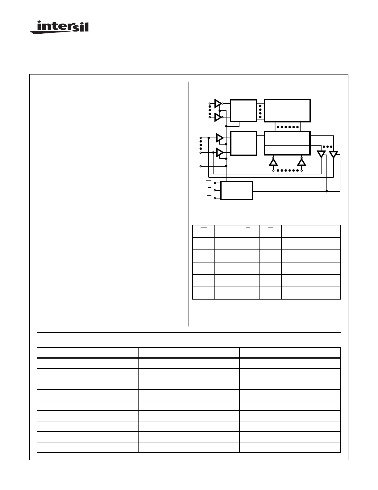
Functional Diagram
AI
ROW
I/O0
I/O7
E2
E1
G
W
E1 E2 G W MODE
X 0 X X Low Power Standby
1 1 X X Disabled
0111Enabled
0101Read
0 1 X 0 Write
ROW
DECODER
INPUT
DATA
CIRCUIT
CONTROL
CIRCUIT
128 X 512
MEMORY ARRAY
COLUMN I/O
COLUMN DECODER
TRUTH TABLE
AI COL
Low power operation is provided by a fully static design. Low
standby power can be achieved without pull-up resistors,
due to the gated input buffer design.
Ordering Information
PART NUMBER TEMPERATURE RANGE PACKAGE
HS1-65647RH-Q -55oC to +125oC 28 Lead SBDIP
HS1-65647RH-8 -55oC to +125oC 28 Lead SBDIP
HS1-65647RH/Proto -55oC to +125oC 28 Lead SBDIP
HS1-65647RH/Sample +25oC 28 Lead SBDIP
HS9-65647RH-Q -55oC to +125oC 28 Lead Ceramic Flatpack
HS9-65647RH-8 -55oC to +125oC 28 Lead Ceramic Flatpack
HS9-65647RH/Proto -55oC to +125oC 28 Lead Ceramic Flatpack
HS9-65647RH/Sample +25oC 28 Lead Ceramic Flatpack
HS9A-65647RH-Q -55oC to +125oC 36 Lead Ceramic Flatpack
CAUTION: These devices are sensitive to electrostatic discharge; follow proper IC Handling Procedures.
http://www.intersil.com or 407-727-9207
| Copyright © Intersil Corporation 1999
824
Spec Number
518729
File Number 2928.2
DB NA
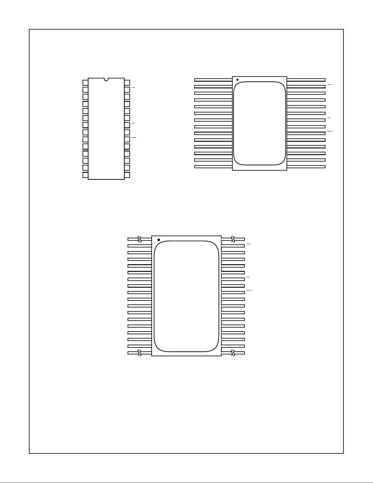
Pinouts
HS1-65647RH 28 LEAD CERAMIC DUAL-IN-LINE
METAL SEAL PACKAGE (SBDIP)
MIL-STD-1835 CDIP2-T28
TOP VIEW
HS-65647RH
HS9-65647RH 28 LEAD CERAMIC METAL
SEAL FLATPACK PACKAGE (FLATPACK)
MIL-STD-1835 CDFP3-F28
TOP VIEW
NC
A12
DQ0
DQ1
DQ2
GND
28
1
2
3
A7
A6
4
A5
5
A4
6
7
A3
A2
8
A1
9
10
A0
11
12
13
14
VDD
W
27
E2
26
A8
25
A9
24
A11
23
G
22
A10
21
20
E1
DQ7
19
DQ6
18
DQ5
17
16
DQ4
DQ3
15
NC
A12
A7
A6
A5
A4
A3
A2
A1
A0
DQ0
DQ1
DQ2
GND
1
2
3
4
5
6
7
8
9
10
11
12
13
14
28
27
26
25
24
23
22
21
20
19
18
17
16
15
VDD
W
E2
A8
A9
A11
G
A10
E1
DQ7
DQ6
DQ5
DQ4
DQ3
HS9A-65647RH 36 LEAD CERAMIC METAL
SEAL FLATPACK P ACKAGE (FLATP ACK)
INTERSIL OUTLINE K36.A
TOP VIEW
NC
A12
DQ0
DQ1
DQ2
GND
DQ0
DQ1
DQ2
GND
1
A7
A6
A5
A4
A3
A2
A1
A0
2
3
4
5
6
7
8
9
10
11
12
13
14
15
16
17
18
36
35
34
33
32
31
30
29
28
27
26
25
24
23
22
21
20
19
VDD
W
E2
A8
A9
A11
G
A10
E1
DQ7
DQ6
DQ5
DQ4
DQ3
DQ0
DQ1
DQ2
GND
825
Spec Number 518729
Specifications HS-65647RH
Absolute Maximum Ratings Reliability Information
Supply Voltage . . . . . . . . . . . . . . . . . . . . . . . . . . . . . . . . . . . . .+7.0V
Input, Output or I/O Voltage . . . . . . . . . . . . GND-0.3V to VDD+0.3V
Storage Temperature Range . . . . . . . . . . . . . . . . . -65oC to +150oC
Junction Temperature. . . . . . . . . . . . . . . . . . . . . . . . . . . . . . +175oC
Lead Temperature (Soldering 10s). . . . . . . . . . . . . . . . . . . . +300oC
Typical Derating Factor. . . . . . . . . . . . 3mA/MHz Increase in IDDOP
ESD Classification . . . . . . . . . . . . . . . . . . . . . . . . . . . . . . . . Class 1
CAUTION: Stresses above those listed in “Absolute Maximum Ratings” may cause permanent damage to the device. This is a stress only rating and operation
of the device at these or any other conditions above those indicated in the operational sections of this specification is not implied.
Operating Conditions
Operating Voltage Range (VDD) . . . . . . . . . . . . . . . +4.5V to +5.5V
Operating Temperature Range (TA) . . . . . . . . . . . . -55oC to +125oC
Input Low Voltage (VIL) . . . . . . . . . . . . . . . . . . . . . . 0V to +0.2VDD
TABLE 1. DC ELECTRICAL PERFORMANCE CHARACTERISTICS
Thermal Resistance θ
28 Lead SBDIP Package. . . . . . . . . . . . . 45oC/W 8.0oC/W
28/36 Lead Ceramic Flatpack Package. . 53.4oC/W 7.4oC/W
Maximum Package Power Dissipation at +125oC Ambient
28 Lead SBDIP Package. . . . . . . . . . . . . . . . . . . . . . . . . . . 1.11W
28/36 Lead Ceramic Flatpack Package. . . . . . . . . . . . . . . . 0.94W
If device power exceeds package dissipation capability, provide heat
sinking or derate linearly at the following rate:
28 Lead SBDIP Package. . . . . . . . . . . . . . . . . . . . . . . .22.2mW/C
28/36 Lead Ceramic Flatpack Package. . . . . . . . . . . . .18.7mW/C
Input High Voltage (VIH). . . . . . . . . . . . . . . . . . . . . .0.8VDD to VDD
Data Retention Supply Voltage. . . . . . . . . . . . . . . . . . . . . . . . . 2.0V
Input Rise and Fall Time. . . . . . . . . . . . . . . . . . . . . . . . . .40ns Max.
JA
θ
JC
(NOTE 1)
PARAMETER SYMBOL
High Level Output
Voltage
Low Level Output
Voltage
High Impedance Output
Leakage Current
Input Leakage Current IIH or IIL VDD = 5.5V, VI = VDD or
Standby Supply Current IDDSB
Enable Supply Current IDDEN VDD = 5.5V, IO = 0mA,
Operating Supply
Current (Note 2)
Data Retention Supply
Current
Functional Tests FT VDD = 4.5V and 5.5V
Noise Immunity
Functional Test
NOTES:
1. All voltages referenced to device GND.
2. Typical IDDOP derating = 3mA/MHz (3mA increase in IDDOP per 1MHz increase in address frequency.)
3. In order for this device to be in low power standby mode. E2 must be disabled (low).
VOH VDD = 4.5V, IO = -5mA
VOL VDD = 4.5V, IO = 8.0mA
IOZL or
IOZH
(Note 3)
IDDOP VDD = 5.5V, IO = 0mA,
IDDDR VDD = 2.0V, IO = 0mA,
FN VDD = 4.5, VIL = 0.2 VDD
CONDITIONS
VI = VDD or GND
VI = VDD or GND
VDD = 5.5V, VO = GND or
VDD, VI = VDD or GND
E1 = VDD, E2 = 0V
GND
VDD = 5.5V, IO = 0mA,
VI = VDD or GND
E1 = VDD, E2 = 0V
VI = VDD or GND
E1 = 0.0V, E2 = VDD
VI = VDD or GND,
E2 = VDD, E1 = 0V,
f = 2MHz
VI = VDD or GND
E1 = VDD, E2 = 0V
VI = VDD or GND, f = 1MHz
VIH = 0.8 VDD, f = 1MHz
GROUP A
SUBGROUPS TEMPERATURE
1, 2, 3 -55oC, +25oC,
+85oC, +125oC
1, 2, 3 -55oC, +25oC,
+85oC, +125oC
1, 3 -55oC, +25oC -10 10 µA
2 +85oC -30 30 µA
2 +125oC -60 60 µA
1, 2, 3 -55oC, +25oC,
+85oC, +125oC
1, 3 -55oC, +25oC - 500 µA
2 +85oC-4mA
2 +125oC - 10 mA
3 -55oC - 77 mA
1 +25oC - 73 mA
2 +85oC, +125oC - 64 mA
3 -55oC - 100 mA
1 +25oC - 86 mA
2 +85oC, +125oC - 75 mA
1, 3 -55oC, +25oC-50µA
2 +85oC-1mA
2 +125oC-4mA
7, 8A, 8B -55oC, +25oC,
+85oC, +125oC
7, 8A, 8B -55oC, +25oC,
+85oC, +125oC
LIMITS
UNITSMIN MAX
VDD-
0.4
- 0.4 V
-1.0 1.0 µA
-- -
-- -
-V
826
Spec Number 518729
Specifications HS-65647RH
TABLE 2. AC ELECTRICAL PERFORMANCE CHARACTERISTICS
LIMITS
(NOTES 1, 2, 3)
PARAMETER SYMBOL
Address Access Time TAVQV VDD = 4.5V 9, 10, 11 -55oC, +25oC, +85oC, +125oC - 50 ns
Output Enable Access Time TGLQV VDD = 4.5V 9, 10, 11 -55oC, +25oC, +85oC, +125oC - 15 ns
CONDITIONS
GROUP A
SUBGROUPS TEMPERATURE
UNITSMIN MAX
Chip Enable Access Time TE1LQV
TE2HQV
Write Recovery Time TWHAX
TE1HAX
TE2LAX
Chip Enable to End-of-Write TE1LE1H
TE2HE2L
Address Setup Time TAVWL
TAVE1L
TAVE2H
Write Enable Pulse Width TWLWH VDD = 4.5V 9, 10, 11 -55oC, +25oC, +85oC, +125oC25 - ns
Data Setup Time TDVWH VDD = 4.5V 9, 10, 11 -55oC, +25oC, +85oC, +125oC30 - ns
TDVE1H
TDVE2L
Data Hold Time TWHDX VDD = 4.5V 9, 10, 11 -55oC, +25oC, +85oC, +125oC0 - ns
Address Hold Time TAVE1H
TAVE2L
TE2LDX
TE1HDX
NOTES:
1. AC measurements tested at worst case VDD. Guaranteed over full operating range.
2. AC measurements assume transition time≤ 5ns; input levels = 0.0V to VDD; timing reference levels = 2.0V; output load = 1 TTL equivalent
load and CL ≥ 50pF, for CL > 50pF, access times are derated 0.15ns/pF.
3. For timing waveforms, see Low Voltage Data Retention and Read/Write Cycles.
VDD = 4.5V 9, 10, 11 -55oC, +25oC, +85oC, +125oC - 50 ns
VDD = 4.5V 9, 10, 11 -55oC, +25oC, +85oC, +125oC0 - ns
VDD = 4.5V 9, 10, 11 -55oC, +25oC, +85oC, +125oC35 - ns
VDD = 4.5V 9, 10, 11 -55oC, +25oC, +85oC, +125oC5 - ns
VDD = 4.5V 9, 10, 11 -55oC, +25oC, +85oC, +125oC30 - ns
VDD = 4.5V 9, 10, 11 -55oC, +25oC, +85oC, +125oC40 - ns
VDD = 4.5V 9, 10, 11 -55oC, +25oC, +85oC, +125oC0 - ns
TABLE 3. ELECTRICAL PERFORMANCE CHARACTERISTICS
LIMITS
PARAMETER SYMBOL CONDITIONS NOTES TEMPERATURE
Input Capacitance CIN VDD = Open, f = 1MHz 1, 2, 4 TA = +25oC - 12 pF
VDD = Open, f = 1MHz 1, 2, 4 TA = +25oC - 12 pF
I/O Capacitance CI/O VDD = Open, f = 1MHz 1, 2, 4 TA = +25oC - 12 pF
VDD = Open, f = 1MHz 1, 2, 4 TA = +25oC - 12 pF
Write Enable to Output in
High Z
TWLQZ VDD = 4.5V and 5.5V 1 -55oC ≤ TA≤ +125oC - 10 ns
UNITSMIN MAX
Spec Number 518729
827
Specifications HS-65647RH
TABLE 3. ELECTRICAL PERFORMANCE CHARACTERISTICS (Continued)
LIMITS
PARAMETER SYMBOL CONDITIONS NOTES TEMPERATURE
Write Enable High to Output ON
Chip Enable to Output ON TE1LQX
Output Enable to Output
ON
Chip Enable to Output in
High Z
Output Disable to Output in
High Z
Output Hold from Address
Change
NOTES:
1. The parameters listed are controlled via design or process parameters and are not directly tested. These parameters are
characterized upon initial design release and upon design changes which would affect these characteristics.
2. Applies to DIP device types only.
3. Applies to Flatpack device types only.
4. All measurements referenced to device GND.
TWHQX VDD = 4.5V and 5.5V 1 -55oC ≤ TA≤ +125oC0 - ns
VDD = 4.5V and 5.5V 1 -55oC ≤ TA≤ +125oC0 - ns
TE2HQX
TGLQX VDD = 4.5V and 5.5V 1 -55oC ≤ TA≤ +125oC0 - ns
TE1HQZ
TE2LQZ
TGHQZ VDD = 4.5V and 5.5V 1 -55oC ≤ TA≤ +125oC - 15 ns
TAXQX VDD = 4.5V and 5.5V 1 -55oC ≤ TA≤ +125oC0 - ns
VDD = 4.5V and 5.5V 1 -55oC ≤ TA≤ +125oC - 15 ns
UNITSMIN MAX
TABLE 4. POST 300K RAD DC ELECTRICAL PERFORMANCE CHARACTERISTICS
LIMITS
PARAMETER SYMBOL CONDITIONS TEMPERATURE
Standby Supply Current IDDSB VDD = 5.5V, IO = 0mA, E1 = VDD,
E2 = 0V, VI = VDD or GND
Enabled Supply Current IDDEN VDD = 5.5V, IO = 0mA, E1 = 0.0V,
E2 = VDD, VI = VDD or GND
Operating Supply Current
(Note 2)
Data Retention Supply Current IDDDR VDD = 2.0V, IO = 0mA, E = VDD +25oC-6mA
NOTES:
1. DC parameters not listed in this table are tested at the +25oC pre-irradiation test limits. All AC parameters are tested at the +25oC preirradiation test limits.
2. Typical IDDOP derating = 3mA/MHz (3mA increase in IDDOP per 1MHz increase in address frequency.)
IDDOP VDD = 5.5V, IO = 0mA, f = 2MHz,
E = 0V,VI = VDD or GND
+25oC - 10 mA
+25oC - 82 mA
+25oC - 100 mA
UNITSMIN MAX
828
Spec Number 518729

HS-65647RH
TABLE 5. BURN-IN DELTA PARAMETERS (+25oC), GROUP B, SUBGROUP 5
PARAMETER SYMBOL DELTA LIMITS
Standby Supply Current IDDSB ±150µA
High Impedance Output Leakage Current IOZH, IOZL ± 2µA
Input Leakage Current IIH, IIL ± 150nA
Low Level Output Voltage VOL ± 60mV
Output High Voltage VOH ± 150mV
TABLE 6. APPLICABLE SUBGROUPS
GROUP A SUBGROUPS
CONFORMANCE
GROUP
Initial Test 100% 5004 1, 7, 9 1 (Note 2) 1, 7, 9
Interim Test 100% 5004 1, 7, 9,∆ 1, ∆ (Note 2) 1, 7, 9
PDA 100% 5004 1, 7, ∆ - 1, 7
Final Test 100% 5004 2, 3, 8A, 8B, 10, 11 - 2, 3, 8A, 8B, 10, 11
Group A (Note 1) Sample 5005 1, 2, 3, 7, 8A, 8B, 9, 10, 11 - 1, 2, 3, 7, 8A, 8B, 9,
Subgroup B5 Sample 5005 1, 2, 3, 7, 8A, 8B, 9, 10, 11, ∆ 1, 2, 3,∆ (Note 2) N/A
Subgroup B6 Sample 5005 1, 7, 9 - N/A
Group C Sample 5005 N/A N/A 1, 2, 3, 7, 8A, 8B, 9,
Group D Sample 5005 1, 7, 9 - 1, 7, 9
Group E, Subgroup 2 Sample 5005 1, 7, 9 - 1, 7, 9
NOTES:
1. Alternate Group A testing in accordance with MIL-STD-883 method 5005 may be exercised.
2. Table 5 parameters only
MIL-STD-883
METHOD
TESTED FOR -Q
RECORDED
FOR -Q TESTED FOR -8
10, 11
10, 11
RECORDED
FOR -8
829
Spec Number 518729

HS-65647RH
Intersil Space Level Product Flow -Q
Wafer Lot Acceptance (All Lots) Method 5007
(Includes SEM)
GAMMA Radiation Verification (Each Wafer) Method 1019,
2 Samples/Wafer, 0 Rejects
100% Nondestructive Bond Pull, Method 2023
Sample - Wire Bond Pull Monitor, Method 2011
Sample - Die Shear Monitor, Method 2019 or 2027
100% Internal Visual Inspection, Method 2010, Condition A
100% Temperature Cycle, Method 1010, Condition C,
10 Cycles
100% Constant Acceleration, Method 2001, Condition per
Method 5004
100% PIND, Method 2020, Condition A
100% External Visual
100% Serialization
100% Initial Electrical Test (T0)
100% Static Burn-In 1, Condition A or B, 72 Hours Min,
NOTES:
1. Failures from subgroup 1, 7 and deltas are used for calculating PDA. The maximum allowable PDA = 5% with no more than 3% of the
2. Radiographic (X-Ray) inspection may be performed at any point after serialization as allowed by Method 5004.
3. Alternate Group A testing may be performed as allowed by MIL-STD-883, Method 5005.
4. Group B and D inspections are optional and will not be performed unless required by the P.O. When required, the P.O. should include
5. Group D Generic Data, as defined by MIL-I-38535, is optional and will not be supplied unless required by the P.O. When required, the
6. Data Package Contents:
tity).
o
+125
C Min, Method 1015
failures from subgroup 7.
separate line items for Group B Test, Group Samples, Group D Test and Group D Samples.
P.O. should include a separate line item for Group D Generic Data. Generic data is not guaranteed to be available and is therefore not
available in all cases.
• Cover Sheet (Intersil Name and/or Logo, P.O. Number , Customer Part Number, Lot Date Code, Intersil Part Number, Lot Number, Quan-
• Wafer Lot Acceptance Report (Method 5007). Includes reproductions of SEM photos with percent of step coverage.
• GAMMA Radiation Report. Contains Cover page, disposition, Rad Dose, Lot Number , Test Package used, Specification Numbers, Test
equipment, etc. Radiation Read and Record data on file at Intersil.
• X-Ray report and film. Includes penetrometer measurements.
• Screening, Electrical, and Group A attributes (Screening attributes begin after package seal).
• Lot Serial Number Sheet (Good units serial number and lot number).
• Variables Data (All Delta operations). Data is identified by serial number. Data header includes lot number and date of test.
• Group B and D attributes and/or Generic data is included when required by the P.O.
• The Certificate of Conformance is a part of the shipping invoice and is not part of the Data Book. The Certificate of Conformance is signed
by an authorized Quality Representative.
100% Interim Electrical Test 1 (T1)
100% Delta Calculation (T0-T1)
100% PDA 1, Method 5004 (Note 1)
100% Dynamic Burn-In, Condition D, 240 Hours, +125
Equivalent, Method 1015
100% Interim Electrical Test 2(T2)
100% Delta Calculation (T0-T2)
100% PDA 2, Method 5004 (Note 1)
100% Final Electrical Test
100% Fine/Gross Leak, Method 1014
100% Radiographic (X-Ray), Method 2012 (Note 2)
100% External Visual, Method 2009
Sample - Group A, Method 5005 (Note 3)
Sample - Group B, Method 5005 (Note 4)
Sample - Group D, Method 5005 (Notes 4 and 5)
100% Data Package Generation (Note 6)
o
C or
830
Spec Number 518729

HS-65647RH
Intersil Space Level Product Flow -8
GAMMA Radiation Verification (Each Wafer) Method 1019,
2 Samples/Wafer, 0 Rejects
Periodic- Wire Bond Pull Monitor, Method 2011
Periodic- Die Shear Monitor, Method 2019 or 2027
100% Internal Visual Inspection, Method 2010, Condition B
100% Temperature Cycle, Method 1010, Condition C,
10 Cycles
100% Constant Acceleration, Method 2001, Condition per
Method 5004
100% External Visual
100% Initial Electrical Test
NOTES:
1. Failures from subgroup 1, 7 are used for calculating PDA. The maximum allowable PDA = 5%.
2. Alternate Group A testing may be performed as allowed by MIL-STD-883, Method 5005.
3. Group B, C and D inspections are optional and will not be performed unless required by the P.O. When required, the P.O. should include
separate line items for Group B Test, Group C Test, Group C Samples, Group D Test and Group D Samples.
4. Group C and/or Group D Generic Data, as defined by MIL-I-38535, is optional and will not be supplied unless required by the P.O. When
required, the P.O. should include a separate line item for Group C Generic Data and/or Group D Generic Data. Generic data is not guaranteed to be available and is therefore not available in all cases.
5. Data Package Contents:
• Cover Sheet (Intersil Name and/or Logo, P.O. Number , Customer Part Number, Lot Date Code, Intersil Part Number, Lot Number, Quan-
tity).
• GAMMA Radiation Report. Contains Cover page, disposition, Rad Dose, Lot Number , Test Package used, Specification Numbers, Test
equipment, etc. Radiation Read and Record data on file at Intersil.
• Screening, Electrical, and Group A attributes (Screening attributes begin after package seal).
• Group B, C and D attributes and/or Generic data is included when required by the P.O.
• The Certificate of Conformance is a part of the shipping invoice and is not part of the Data Book. The Certificate of Conformance is signed
by an authorized Quality Representative.
100% Dynamic Burn-In, Condition D, 160 Hours, +125oC or
Equivalent, Method 1015
100% Interim Electrical Test
100% PDA, Method 5004 (Note 1)
100% Final Electrical Test
100% Fine/Gross Leak, Method 1014
100% External Visual, Method 2009
Sample - Group A, Method 5005 (Note 2)
Sample - Group B, Method 5005 (Note 3)
Sample - Group C, Method 5005 (Notes 3 and 4)
Sample - Group D, Method 5005 (Notes 3 and 4)
100% Data Package Generation (Note 5)
831
Spec Number 518729

Timing Waveforms
HS-65647RH
TAVAX
E1
E2
A
Q
ADDRESS 1
TAVQV
TAXQX
DATA 1
ADDRESS 2
DATA 2
FIGURE 1. READ CYCLE I: W, E2 HIGH; G, E1 LOW
TAVAX
A
TAVQV
TE1LQV
TE1LQX
TE2HQV
TE2HQX
G
TGLQV
TGLQX
Q
TE1HQZ
TE2LQZ
TGHQZ
E1
E2
FIGURE 2. READ CYCLE II: W HIGH
TAVAX
A
TAVWL TWLWH TWHAX
W
TWHQX
TDVWH
D
TWLQZ
Q
TWHDX
FIGURE 3. WRITE CYCLE I: LATE WRITE
832
Spec Number 518729

HS-65647RH
Timing Waveforms
A
W
E1
E2
D
A
W
(Continued)
TAVAX
TAVE1L
TE1LE1H
TAVE2H
TDVE1H
TE1HDX
FIGURE 4. WRITE CYCLE II: EARLY WRITE - CONTROLLED BY E1
TAVAX
TAVE2H
TE2HE2L
TAVE2L
TE1HAX
TE2LAX
E1
E2
TDVE2L TE2LDX
D
FIGURE 5. WRITE CYCLE III: EARLY WRITE - CONTROLLED BY E2
833
Spec Number 518729

Performance Curves
HS-65647RH TYPICAL PERFORMANCE CHARACTERISTICS
TA = +25oC, Unless Otherwise Specified
13
12
11
10
9
8
7
6
IDDSB (mA)
5
4
3
2
1
0
0 200 400 600 800 1000 1200 1400
TOTAL DOSE (KRAD)
FIGURE 6 FIGURE 7
10
9
8
7
6
5
4
IDDSB (mA)
3
2
1
0
-60 -40 -20 0 20 40 60 80 100 120
TEMPERATURE (oC)
FIGURE 8 FIGURE 9
120
110
100
90
80
70
60
IDDOP (mA)
50
40
30
20
-60 -40 -20 0 20 40 60 80 100 120
TEMPERATURE (
FIGURE 10 FIGURE 11
o
C)
HS-65647RH
7
6
5
4
3
IDDSB (mA)
2
1
0
100
90
80
70
60
50
40
IDDEN (mA)
30
20
10
0
106
102
98
94
90
86
82
78
IDDOP (mA)
74
70
66
62
58
0.1 0.1 10 100
ANNEAL TIME (HOURS)
-60 -40 -20 0 20 40 60 80 100 120
TEMPERATURE (
012345678 910
FREQUENCY (MHz)
o
C)
834
Spec Number 518729

Burn-In Circuits
HS-65647RH 28 LEAD FLATPACK AND CERAMIC DIP
F13
F14
F14
F14
1
NC
F8
F7
F6
F5
F4
F3
F2
F1
R2
R2
R2
NC
2
A12
3
A7
4
A6
5
A5
6
A4
7
A3
8
A2
9
A1
10
A0
11
DQ0
12
DQ1
13
DQ2
14
VSS
VDD
A11
A10
DQ7
DQ6
DQ5
DQ4
DQ3
28
27
W
26
E2
25
A8
24
A9
23
22
G
21
20
E1
19
18
17
16
15
HS-65647RH
VDD
F0
F9
F10
F12
F0
F11
R2
F14
R2
F14
R2
F14
R2
F14
R2
F14
HS-65647RH 28 LEAD FLATPACK AND CERAMIC DIP
VDD
NC
NC
NC
NC
1
NC
2
A12
3
A7
4
A6
5
A5
6
A4
7
A3
8
A2
9
A1
10
A0
11
DQ0
12
DQ1
13
DQ2
14
VSS
VDD
A11
A10
DQ7
DQ6
DQ5
DQ4
DQ3
28
27
W
26
E2
25
A8
24
A9
23
22
G
21
20
E1
19
NC
18
NC
17
NC
16
NC
15
NC
DYNAMIC CONFIGURATION
NOTES:
1. VDD = 5.5V Min
2. R = 10kΩ± 10%, except R2 = 47kΩ± 10%
3. VIH: VDD ± 0.5V, VIL: 0.4V ± 0.4V
4. F0 = 100kHz ± 10%, 50% Duty Cycle
5. F1 = F0/2; F2 = F1/2; F3 = F2/2; . . . F14 = F13/2
6. F0 = inverted F0
HS-65647RH 36 LEAD FLATPACK
F13
F14
F14
F14
1
VSS
2
VDD
3
NC
F8
F7
F6
F5
F4
F3
F2
F1
R2
R2
R2
NC
NC
4
A12
5
A7
6
A6
7
A5
8
A4
9
A3
10
A2
11
A1
12
A0
13
DQ0
14
DQ1
15
DQ2
16
NC
17
VDD
18
VSS
VSS
VDD
NC
A11
A10
DQ7
DQ6
DQ5
DQ4
DQ3
VDD
VSS
36
35
34
33
W
32
E2
31
A8
30
A9
29
28
G
27
26
E1
25
24
23
22
21
20
19
NC
STATIC CONFIGURATION
NOTES:
1. VDD = 5.5V Min
2. R = 10kΩ± 10%
HS-65647RH 36 LEAD FLATPACK
VDD
1
VSS
2
VDD
3
NC
F0
F9
F10
F12
F0
F11
R2
F14
R2
F14
R2
F14
R2
F14
R2
F14
NC
NC
NC
NC
NC
4
A12
5
A7
6
A6
7
A5
8
A4
9
A3
10
A2
11
A1
12
A0
13
DQ0
14
DQ1
15
DQ2
16
NC
17
VDD
18
VSS
VSS
VDD
NC
A8
A9
A11
A10
DQ7
DQ6
DQ5
DQ4
DQ3
VDD
VSS
36
35
34
33
W
32
E2
31
30
29
28
G
27
26
E1
25
24
23
22
21
20
19
VDD
NC
NC
NC
NC
NC
NC
DYNAMIC CONFIGURATION
NOTES:
1. VDD = 5.5V Min
2. R = 10kΩ± 10%, except R2 = 4.7kΩ± 10%
3. VIH: VDD ± 0.5V, VIL: 0.4V ± 0.4V
4. F0 = 100kHz ± 10%, 50% Duty Cycle
5. F1 = F0/2; F2 = F1/2; F3 = F2/2; . . . F14 = F13/2
6. F0 = Inverted F0
STATIC CONFIGURATION
NOTES:
1. VDD = 5.5V Min
2. R = 10kΩ± 10%
Spec Number 518729
835

Irradiation Circuit
HS-65647RH
HS-65647RH (8K x 8 TSOS4 SRAM) 28 LEAD CERAMIC DIP
VDD
NOTES:
1. VDD = 5.5V ± 0.5V
R = 10kΩ± 10%
2. Group E sample size is two die/wafer.
NC
NC
1
A12
2
A7
3
A6
4
A5
5
A4
6
A3
7
A2
8
A1
9
A0
10
DQ0
11
DQ1
12
DQ2
13
VSS
14
VDD
E2
A8
A9
A11
A10
E1
DQ7
DQ6
DQ5
DQ4
DQ3
28
W
27
26
25
24
23
G
22
21
20
19
18
17
16
15
Test Patterns
MARCH (II)PATTERN
After a background of zeros is written, each cell (from beginning to end in sequence) is read, written to a one and
reread. When the array is full of ones each cell (from the end
to the beginning) is read, restored to a zero and reread.
After this the pattern is repeated but with complemented
data.
MASEST PATTERN (Multiple Address Select Pattern)
A checkerboard pattern is written into the memory. Then the
first cell is read, then its binary address complement is read.
The second cell is read and then its binary address complement is read. This pattern of incrementing the address and
then reading its binary address complement is repeated until
the entire memory is read.
This is then repeated but using a checkerboard bar pattern.
GALROW PATTERN (Row Galloping Pattern)
After a background of zeros is written into the memory a one
is written into the first cell. It is then read alternately with
each other cell in the row. The test cell is then rewritten back
to a zero. The test cell is then incremented and the
sequence is repeated until all cells in the memory have been
used as a test cell.
This is pattern then repeated but using complemented data.
GALCOL PATTERN (Column Galloping Pattern)
After a background of zeros is written into the memory a one
is written into the first cell. It is then read alternately with
each other cell in the column. The test cell is then rewritten
back to a zero. The test cell is then incremented and the
sequence is repeated until all cells in the memory have been
used as a test cell.
This is pattern then repeated but using complemented data.
CHECKERBOARD PATTERN and CHECKERBOARD
BAR
A checkerboard is written (101010) into the memory and
then the pattern is read back. This is then repeated but using
complemented data.
836
Spec Number
518729

Metallization Topology
DIE DIMENSIONS:
313 x 291 x 21 ±1mils
METALLIZATION:
Type: Al/Si/Cu
Metal 1 Thickness: 7500
Å ± 2kÅ
Metal 2 Thickness: 10kÅ ± 2kÅ
Metallization Mask Layout
HS-65647RH
GLASSIVATION:
Type: SiO
Thickness: 8kÅ ± 1kÅ
WORST CASE CURRENT DENSITY:
1.5 x 10
HS-65647RH
2
5
Amps/cm
2
VSS
NC
(7) A3
(6) A4
(5) A5
(4) A6
(3) A7
(2) A12
(28) VDD
(27) W
(26) E2
(25) A8
(24) A9
(23) A11
(22) G
NC
VSS
VDD
NC
A2 (8)
A1 (9)
A0 (10)
VDD
VDD
DQ0 (11)
DQ1 (12)
DQ2 (13)
VSS (14)
DQ3 (15)
DQ4 (16)
D15 (17)
DQ6 (18)
DQ7 (19)
E (20)
NC
A10 (21)
Spec Number 518729
837

Packaging
HS-65647RH
e
PIN NO. 1
ID AREA
-A- -B-
b
E1
0.004 H A - BMD
Q
A
-C-
SEATING AND
BASE PLANE
S S
L
E3 E3
c1
M
SECTION A-A
E
LEAD FINISH
BASE
METAL
b1
M
(b)
0.036 H A - BMD
(c)
-D-
LE2
A
A
S1
S S
C
-H-
NOTES:
1. Index area: A notch or a pin one identification mark shall be located adjacent to pin one and shall be located within the shaded
area shown. The manufacturer’s identification shall not be used
as a pin one identification mark. Alternately, a tab (dimension k)
may be used to identify pin one.
2. If a pin one identification mark is used in addition to a tab, the limits of dimension k do not apply.
3. This dimension allows for off-center lid, meniscus, and glass
overrun.
4. Dimensions b1 and c1 apply to lead base metal only . Dimension
M applies to lead plating and finish thickness. The maximum limits of lead dimensions b and c or M shall be measured at the centroid of the finished lead surfaces, when solder dip or tin plate
lead finish is applied.
5. N is the maximum number of terminal positions.
6. Measure dimension S1 at all four corners.
7. For bottom-brazed lead packages, no organic or polymeric materials shall be molded to the bottom of the package to cover the
leads.
8. Dimension Q shall be measured at the point of exit (beyond the
meniscus) of the lead from the body. Dimension Q minimum
shall be reduced by 0.0015 inch (0.038mm) maximum when solder dip lead finish is applied.
9. Dimensioning and tolerancing per ANSI Y14.5M - 1982.
10. Controlling dimension: INCH.
K36.A
36 LEAD CERAMIC METAL SEAL FLATPACK PACKAGE
INCHES MILLIMETERS
SYMBOL
D
A - 0.138 - 3.51 -
b 0.006 0.013 0.15 0.33 -
b1 0.006 0.010 0.15 0.25 -
c 0.004 0.011 0.10 0.28 -
c1 0.004 0.008 0.10 0.20 -
D 0.620 0.640 15.75 16.26 3
E 0.620 0.640 15.75 8.64 E1 - 0.660 - 16.76 3
E2 0.470 0.490 11.94 12.45 E3 0.030 - 0.76 - 7
e 0.025 BSC 0.64 BSC k----L 0.240 0.280 6.10 7.11 -
Q 0.026 0.045 0.66 1.14 8
S1-----
M - 0.0015 - 0.04 -
N36 36-
NOTESMIN MAX MIN MAX
Rev. 0 5/18/94
838
Spec Number 518729

HS-65647RH
All Intersil semiconductor products are manufactured, assembled and tested under ISO9000 quality systems certification.
Intersil products are sold by description only. Intersil Corporation reserves the right to make changes in circuit design and/or specifications at any time without
notice. Accordingly, the reader is cautioned to verify that data sheets are current before placing orders. Information furnished by Intersil is believed to be accurate
and reliable. However, no responsibility is assumed by Intersil or its subsidiaries for its use; nor for any infringements of patents or other rights of third parties which
may result from its use. No license is granted by implication or otherwise under any patent or patent rights of Intersil or its subsidiaries.
For information regarding Intersil Corporation and its products, see web site http://www.intersil.com
Sales Office Headquarters
NORTH AMERICA
Intersil Corporation
P. O. Box 883, Mail Stop 53-204
Melbourne, FL 32902
TEL: (407) 724-7000
FAX: (407) 724-7240
EUROPE
Intersil SA
Mercure Center
100, Rue de la Fusee
1130 Brussels, Belgium
TEL: (32) 2.724.2111
FAX: (32) 2.724.22.05
839
ASIA
Intersil (Taiwan) Ltd.
Taiwan Limited
7F-6, No. 101 Fu Hsing North Road
Taipei, Taiwan
Republic of China
TEL: (886) 2 2716 9310
FAX: (886) 2 2715 3029
Spec Number
 Loading...