

March 1996
HS-3374RH
Radiation Hardened
8-Bit Bidirectional CMOS/TTL Level Converter
Features
• Devices QML Qualified in Accordance with MIL-PRF-38535
• Detailed Electrical and Screening Requirements are
Contained in SMD# 5962-9XXXX and Intersil’ QM Plan
• Radiation Hardened EPI-CMOS
- Total Dose 1 x 10
- Latch-Up Immune > 1 x 10
5
RAD(Si)
12
RAD (Si)/s (Note 1)
• Low Propagation Delay Time
- Typical CMOS to TTL Pre-RAD 40ns
- Typical CMOS to TTL Post 100K RAD 40ns
- Typical TTL to CMOS Pre-RAD 50ns
- Typical TTL to CMOS Post 100K RAD 50ns
• Low Standby Power
• +10V CMOS and +5V TTL Power Supply Inputs
• Eight Non-inverting Three-State Input/Output Channels
• No External TTL Input Pull-Up Resistors Required
• High TTL Sink Current
• Equivalent to Sandia SA2996
o
• Military Temperature Range -55
C to +125oC
Description
The Intersil HS-3374RH is a radiation hardened 8-bit
bidirectional level converter designed to interface CMOS logic
levels with TTL logic levels in radiation hardened bus oriented
systems. The HS-3374RH is fabricated using a radiation
hardened EPI-CMOS process and features eight parallel
bidirectional buffer/level converters.
Two control inputs, ENABLE and DISABLE, are used to determine the direction of data flow, and to set both the in puts and
outputs in the high impedance state. The control inputs may be
driven by either TTL or CMOS logic drivers capable of sinking
one standard TTL load.
The HS-3374RH is a non-inverting version of the industry
standard CD40116. The non-inverting outputs of the
HS-3374RH reduce PC board chip count by eliminating the
need to restore data back to a non-inverted format.
NOTE:
1. For operation at 10V and transient le vels abo ve 1 x 10¹⁰ RAD (Si)/s,
please refer to Application Note 401.
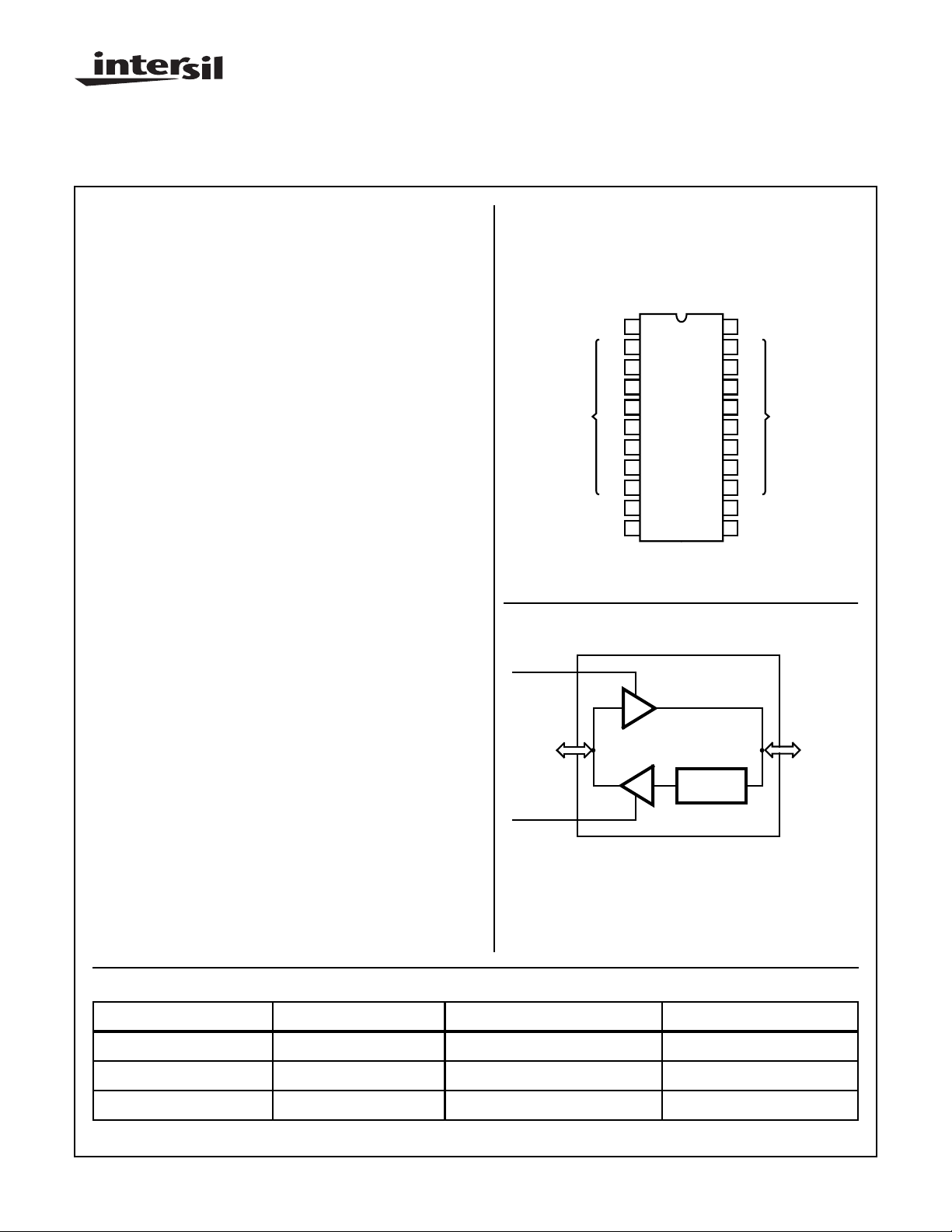
Pinout
HS-3374RH
MIL-STD-1835, CDIP2-T22
(SBDIP)
TOP VIEW
VDD
1
A0
2
A1
3
A2
4
A3
INPUT/OUTPUT
CMOS
ENABLE
A4
A5
A6
A7
GND
5
6
7
8
9
10
11
Functional Diagram
DISABLE
13
CMOS
IN/OUT
ENABLE
10
88
2-9
LEVEL
SHIFTER
22
21
20
19
18
17
16
15
14
13
12
VCC
B0
B1
B2
B3
TTL
INPUT/OUTPUT
B4
B5
B6
B7
DISABLE
NC
VDD = 1
VCC = 22
GND = 11
14-21
TTL
OUT (IN)
Ordering Information
PART NUMBER TEMPERA TURE RANGE SCREENING LEVEL PACKAGE
5962R9XXXX01QRC
5962R9XXXX01VRC
HS1-3374 (SAMPLE)
CAUTION: These devices are sensitive to electrostatic discharge; follow proper IC Handling Procedures.
http://www.intersil.com or 407-727-9207
-55oC to +125oC
-55oC to +125oC
+25oC
| Copyright © Intersil Corporation 1999
MIL-PRF-38535 Level Q
MIL-PRF-38535 Level V
Sample
1
22 Lead SBDIP
22 Lead SBDIP
22 Lead SBDIP
Spec Number 518052
File Number 3038.1
Specifications HS-3374RH
Absolute Maximum Ratings Thermal Information
Supply Voltage . . . . . . . . . . . . . . . . . . . . . . . . . . . . . . . . . . . .+11.0V
I/O Voltage Applied. . . . . . . . . . . . . . . . . . . GND-0.3V to VDD+0.3V
Storage Temperature Range . . . . . . . . . . . . . . . . . -65oC to +150oC
Junction Temperature. . . . . . . . . . . . . . . . . . . . . . . . . . . . . . +175oC
Lead Temperature (Soldering 10s). . . . . . . . . . . . . . . . . . . . +300oC
ESD Classification . . . . . . . . . . . . . . . . . . . . . . . . . . . . . . . . Class 1
CAUTION: Stresses above those listed in “Absolute Maximum Ratings” may cause permanent damage to the device. This is a stress only rating and operation
of the device at these or any other conditions above those indicated in the operational sections of this specification is not implied.
Operating Conditions
Operating Voltage Range VDD . . . . . . . . . . . . . +9.5V to +10.5V
VCC . . . . . . . . . . . . +4.75V to +5.25V
Operating Temperature Range. . . . . . . . . . . . . . . . -55oC to +125oC
Input Voltage Range
Data Inputs (CMOS) . . . . . . . . . . . . . . . . . . .GND-0.3 to VDD+0.3
Data Inputs (TTL) . . . . . . . . . . . . . . . . . . . . .GND-0.3 to VCC+0.3
Enable, Disable Inputs . . . . . . . . . . . . . . . . .GND-0.3 to VDD+0.3
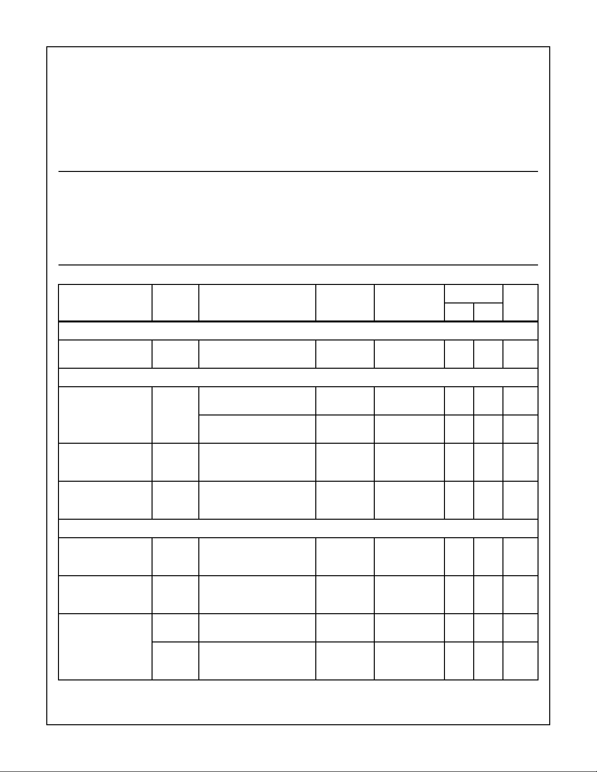
TABLE 1. DC ELECTRICAL PERFORMANCE CHARACTERISTICS
Thermal Resistance (Typical) θJA(oC/W) θJC (oC/W)
SBDIP Package. . . . . . . . . . . . . . . . . . 74.8 12.3
Maximum Package Power Dissipation at +125oC
SBDIP Package. . . . . . . . . . . . . . . . . . . . . . . . . . . . . . . . . .0.67W
If Device Power Exceeds Package Dissipation Capability, Provide
Heat Sinking or Derate Linearly at the Following Rate:
SBDIP Package. . . . . . . . . . . . . . . . . . . . . . . . . . . . . .13.4mW/oC
Input Low Voltage (CMOS) . . . . . . . . . . . . . . . . . . . . . . . GND to 1V
Input High Voltage (CMOS). . . . . . . . . . . . . . . . . .VDD-1.0V to VDD
Input Low Voltage (TTL) . . . . . . . . . . . . . . . . . . . . . . . . . . . . . . 0.8V
Input High Voltage (TTL). . . . . . . . . . . . . . . . . . . . . . . . . . . . . . 2.8V
PARAMETER SYMBOL CONDITIONS
ENABLE AND DISABLE IINPUTS
Input Leakage Current IIH CMOS VDD = 10.5V, VCC = 5.25V,
VIN = 10.5V, Floating Outputs
TTL INPUT TO CMOS OUTPUTS
Input Leakage Current IIL IIH VDD = 10.5V, VCC = 5.25V,
VIN = 0.8V, Other Inputs at 2.8V
VDD = 10.5V, VCC = 5.25V,
VIN = 2.8V, other Inputs = 0.8V
High Level Output
Voltage
Low level output
Voltage
CMOS to TTL OUTPUTS
High Level Output
Voltage
VOH VDD = 9.5V, VCC = 4.75V,
VIH = 2.8V, VIL = 0.8V,
IOH = -2.0mA
VOL VDD = 10.5V, VCC = 5.25V,
VIH = 2.8V, VIL 0.8V,
IOL = 2.0mA
VOH VDD = 9.5, VCC = 4.75V,
VIH = 8.5V, VIL = 1.0V,
IOH = -2.0mA
GROUP A
SUBGROUPS TEMPERATURE
1, 2, 3 -55oC, +25oC,
+125oC
1, 2, 3 -55oC, +25oC,
+125oC
1, 2, 3 -55oC, +25oC,
+125oC
1, 2, 3 -55oC, +25oC,
+125oC
1, 2, 3 -55oC, +25oC,
+125oC
1, 2, 3 -55oC, +25oC,
+125oC
LIMITS
UNITSMIN MAX
-1µA
-1 - µA
-1µA
9- V
- 0.5 V
3- V
Low Level Output
Voltage
Output Leakage
Current
VOL VDD = 10.5V, VCC = 5.25V,
VIH = 9.5V, VIL = 1.0V,
IOL = 11mA
IOZL VDD = 10.5V, VCC = 5.25V,
VIN = 0V, All other pins high
IOZH VDD = 10.5V, VCC = 5.25V,
VIN = 2.8V, All other pins at
GND
1, 2, 3 -55oC, +25oC,
+125oC
1, 2, 3 -55oC, +25oC,
+125oC
1, 2, 3 -55oC, +25oC,
+125oC
- 0.4 V
-10 - µA
-10µA
Spec Number 518052
2

Specifications HS-3374RH
TABLE 1. DC ELECTRICAL PERFORMANCE CHARACTERISTICS (Continued)
PARAMETER SYMBOL CONDITIONS
Functional Tests FT CMOS:
1.) VDD = 10.5V, VCC = 5.25V
2.) VDD = 9.5V, VCC = 4.75V,
VIH = VDD-1V, VIL = 1V
TTL:
1.) VDD = 10.5V, VCC = 5.25V
2.) VDD = 9.5V, VCC = 4.75V,
VIH = 2.8V, VIL = 0.8V
Static Current 1 SIDD1 VDD = 10.5V, VCC = 5.25V,
EN = 2.8V, DISABLE = 2.8V,
Floating Outputs
Static Current 2 SIDD2 VDD = 10.5V, VCC = 5.25V, EN
= 0V, DISABLE = 2.8V, Floating
Outputs
Static Current SICC VDD = 10.5, VCC = 5.25V,
EN = 0V, DISABLE = 2.8V,
Floating Output, Measure VCC
pin
TABLE 2. AC ELECTRICAL PERFORMANCE CHARACTERISTICS
GROUP A SUB-
PARAMETER SYMBOL
GROUPS TEMPERATURE
GROUP A
SUBGROUPS TEMPERATURE
7, 8A, 8B -55oC, +25oC,
+125oC
1, 2, 3 -55oC, +25oC,
+125oC
1, 2, 3 -55oC, +25oC,
+125oC
1, 2, 3 -55oC, +25oC,
+125oC
LIMITS
UNITSMIN MAX
-- -
- 300 µA
- 100 µA
-5µA
LIMITS
UNITSMIN MAX
Propagation Delay Times CMOS/TTL
Data In to Data Out
Propagation Delay Times CMOS Data
In to Data Out
Propagation Delay Times CMOS/TTL
Data In to Data Out
Propagation Delay Time TTL/CMOS
Data In to Data Out
Transition Time CMOS/TTL
Input/Output
Transition Time CMOS/TTL
Input/Output
Transition Time CMOS/TTL
Input/Output
Transition Time CMOS/TTL
Input/Output
Propagation Delay Time TTL/CMOS
Enable to CMOS Out
Propagation Delay Time TTL/CMOS
Enable to CMOS Out
Propagation Delay Time TTL/CMOS
Enable to CMOS Out
TPHLCT 9, 10, 11 -55oC, +25oC, +125oC - 40 ns
TPLHCT 9, 10, 11 -55oC, +25oC, +125oC - 50 ns
TPHLTC 9, 10, 11 -55oC, +25oC, +125oC - 85 ns
TPLHTC 9, 10, 11 -55oC, +25oC, +125oC - 70 ns
TTHLCT 9, 10, 11 -55oC, +25oC, +125oC - 20 ns
TTLHCT 9, 10, 11 -55oC, +25oC, +125oC - 70 ns
TTHLTC 9, 10, 11 -55oC, +25oC, +125oC - 50 ns
TTLHTC 9, 10, 11 -55oC, +25oC, +125oC - 50 ns
TPHZTC 9, 10, 11 -55oC, +25oC, +125oC - 90 ns
TPZHTC 9, 10, 11 -55oC, +25oC, +125oC - 90 ns
TPLZTC 9, 10, 11 -55oC, +25oC, +125oC - 85 ns
Spec Number 518052
3

Specifications HS-3374RH
TABLE 2. AC ELECTRICAL PERFORMANCE CHARACTERISTICS (Continued)
GROUP A SUB-
PARAMETER SYMBOL
Propagation Delay Time TTL/CMOS
Enable to CMOS Out
Propagation Delay Time CMOS/TTL
Disable to TTL Out
Propagation Delay Time CMOS/TTL
Disable to TTL Out
Propagation Delay Time CMOS/TTL
Disable to TTL Out
Propagation Delay Time CMOS/TTL
Disable to TTL Out
NOTE: Timings are measured with the following conditions: CL = 100pF, VDD = 9.5V, VCC = 4.75V, VIH = 8.5V (2.8V), VIL = 1.0V (0.8V).
TABLE 3. ELECTRICAL PERFORMANCE CHARACTERISTICS
PARAMETER SYMBOL CONDITIONS TEMPERATURE
Input, Output Capacitance CMOS
TPZLTC 9, 10, 11 -55oC, +25oC, +125oC - 90 ns
TPHZCT 9, 10, 11 -55oC, +25oC, +125oC - 70 ns
TPZHCT 9, 10, 11 -55oC, +25oC, +125oC - 130 ns
TPLZCT 9, 10, 11 -55oC, +25oC, +125oC - 120 ns
TPZLCT 9, 10, 11 -55oC, +25oC, +125oC - 125 ns
VDD = Open, f = 1MHz, All Measure-
CI/O
ments Referenced to Device Ground
GROUPS TEMPERATURE
+25oC - 13 pF
LIMITS
UNITSMIN MAX
LIMITS
UNITSMIN MAX
Input Capacitance CIN VDD = Open, f = 1MHz, All Measure-
ments Referenced to Device Ground
Input, Output Capcitance TTL
CI/O
NOTE: The parameters listed in Table 3 are controlled via design or process parameters and are not directly tested. These parameters
are characterized upon initial design release and upon design changes which would affect these characteristics.
VDD = Open, f = 1MHz, All Measurements Referenced to Device Ground
+25oC - 15 pF
+25oC - 17 pF
Spec Number 518052
4

Functional Block Diagram
1 OF 8 IDENTICAL CIRCUITS
HS-3374RH
VDD
VDD
VCC
2 (3, 4, 5, 6, 7, 8, 9)
A1 CMOS
INPUT (OUTPUT)
GND
VDD
D
LEVEL
SHIFTER
E
INPUT (OUTPUT) OUTPUT (INPUT)
TERMINAL
DATA
NUMBER DATA
A0 2 B0 21
A1 3 B1 20
A2 4 B2 19
A3 5 B3 18
A4 6 B4 17
A5 7 B5 16
A6 8 B6 15
A7 9 B7 14
VCC
B1 TTL
OUTPUT
(INPUT)
21 (20, 19,
18, 17, 16,
15, 14)
GND
TERMINAL
NUMBER
DISABLE
13
ENABLE
10
GND
GND
VDD
LEVEL
SHIFTER
LEVEL
SHIFTER
D
E
NOTES:
1. Enable and disable are TTL type inputs
2. D and E outputs are common to all 8 channels
TRUTH TABLE
ENABLE DISABLE FUNCTION
X 0 Convert CMOS Level to TTL Level
1 1 Convert TTL Level to CMOS Level
0 1 High Impedance (Z)
0 = Low Level 1 = High Level X = Don’t Care
Z = High Impedance on Both CMOS and TTL sides.
NOTE: An important caveat that is applicable to CMOS devices in
general is that unused inputs should never be left floating. This rule
applies to inputs connected to a three-state bus. The need for
external pull-up resistors during three-state bus conditions is
eliminated by the presence of regenerative latches on the follo wing
HS-3374RH pins: A0 - 7.
The functional block diagram depicts one of these pins with the
regenerative latch. When the CMOS driver assumes the high
impedance state, the latch holds the bus in whatever logic state
(high or low) it was before the three-state condition. A transient
drive current of ±1.5mA at VDD/2 ±0.5V for 10ns is required to
switch the latch. Thus, CMOS device inputs connected to the bus
are not allowed to float during three-state conditions.
* WARNING: Do not activate the Disable input by hardwiring to any
TTL input pins. This is an incorrect mode of operation.
Spec Number 518052
5

Metallization Topology
DIE DIMENSIONS:
89.4 mils x 76.0 mils x 14 mils ±1 mil
METALLIZATION:
Type: AlSi
Thickness: 8k
Å ±1kÅ
GLASSIVATION:
Type: SiO2
Thickness: 11k
Å ±2kÅ
Metallization Mask Layout
HS-3374RH
HS-3374RH
A2 (4)
A3 (5)
A4 (6)
A5 (7)
A6 (8)
A7 (9)
(3) A1
(2) A0
(1) VDD
(22) VCC
(21) B0
(20) B1
(19) B2
(18) B3
(17) B4
(16) B5
(15) B6
(14) B7
GND (11)
ENABLE (10)
DISABLE (13)
All Intersil semiconductor products are manufactured, assembled and tested under ISO9000 quality systems certification.
Intersil products are sold by description only. Intersil Cor poration reserves the right to make changes in circuit design and/or specifications at any time without
notice. Accordingly, the reader is cautioned to verify that data sheets are current before placing orders. Information furnished by Intersil is believed to be accurate
and reliable. However, no responsibility is assumed by Intersil or its subsidiaries for its use; nor for any infringements of patents or other rights of third parties which
may result from its use. No license is granted by implication or otherwise under an y patent or patent rights of Intersil or its subsidiaries.
For information regarding Intersil Corporation and its products, see web site http://www.intersil.com
Spec Number 518052
6
 Loading...