

HS-2700RH
Data Sheet August 1999
Low Power, High Performance Radiation
Hardened Operational Amplifier
HS-2700RH is radiation hardened internally compensated
operational amplifiers which employ dielectric isolation to
achieve excellent DC and dynamic performance with very
low quiescent power consumption.
DC performance of the amplifier input is characterized by
high CMRR (106dB), low offset voltage (0.5mV), along with
low bias and offset current (5.0nA and 2.5nA respectively).
These input specifications, in conjunction with offset null
capability and open-loop gain of 300,000V/V, enable
HS-2700RH to provide accurate, high-gain signal
amplification. Gain bandwidth 1MHz and slew rate of20V/µs
allow for processing of fast, wideband signals. Input and
output signal amplitudes of at least ±11V can be
accommodated while providing output drive capability of
10mA. For maximum reliability, the output is protected in the
event of short circuits to ground.
The amplifier operates from a wide range of supplies (±5.5V
to ±20V) with a maximum quiescent supply drain of only
150µA. HS-2700RH is therefore, ideally suited to low-power
instrumentation and filtering applications that require fast,
accurate response over a wide range of signal frequency.
Specifications for Rad Hard QML devices are controlled
by the Defense Supply Center in Columbus (DSCC). The
SMD numbers listed here must be used when ordering.
Detailed Electrical Specifications for these devices are
contained in SMD 5962-95670. A “hot-link” is provided
on our homepage for downloading.
www.intersil.com/spacedefense/space.asp
File Number 3624.2
Features
• Electrically Screened to SMD # 5962-95670
• QML Qualified per MIL-PRF-38535 Requirements
• Low Power Supply Current. . . . . . . . . . . . . . 150µA (Max)
90µA (Typ)
• High CMRR . . . . . . . . . . . . . . . . . . . . . . . . . . .86dB (Min)
106dB (Typ)
• Low Input Bias Current. . . . . . . . . . . . . . . . . . .20nA (Min)
5nA (Typ)
• Low Offset Current. . . . . . . . . . . . . . . . . . . . . .10nA (Min)
2.5nA (Typ)
• Total Dose . . . . . . . . . . . . . . . . . . . . . . . . 1 x 10
4
RAD(Si)
Applications
• High Gain Amplifier
• Instrumentation Amplifiers
• Active Filters
• Telemetry Systems
• Battery-Powered Equipment
Ordering Information
INTERNAL
ORDERING NUMBER
5962D9567002VCA HS1-2700RH-Q -55 to 125
5962D9567002VCC HS1B-2700RH-Q -55 to 125
5962D9567002VGA HS2-2700RH-Q -55 to 125
MKT. NUMBER
TEMP. RANGE
(oC)
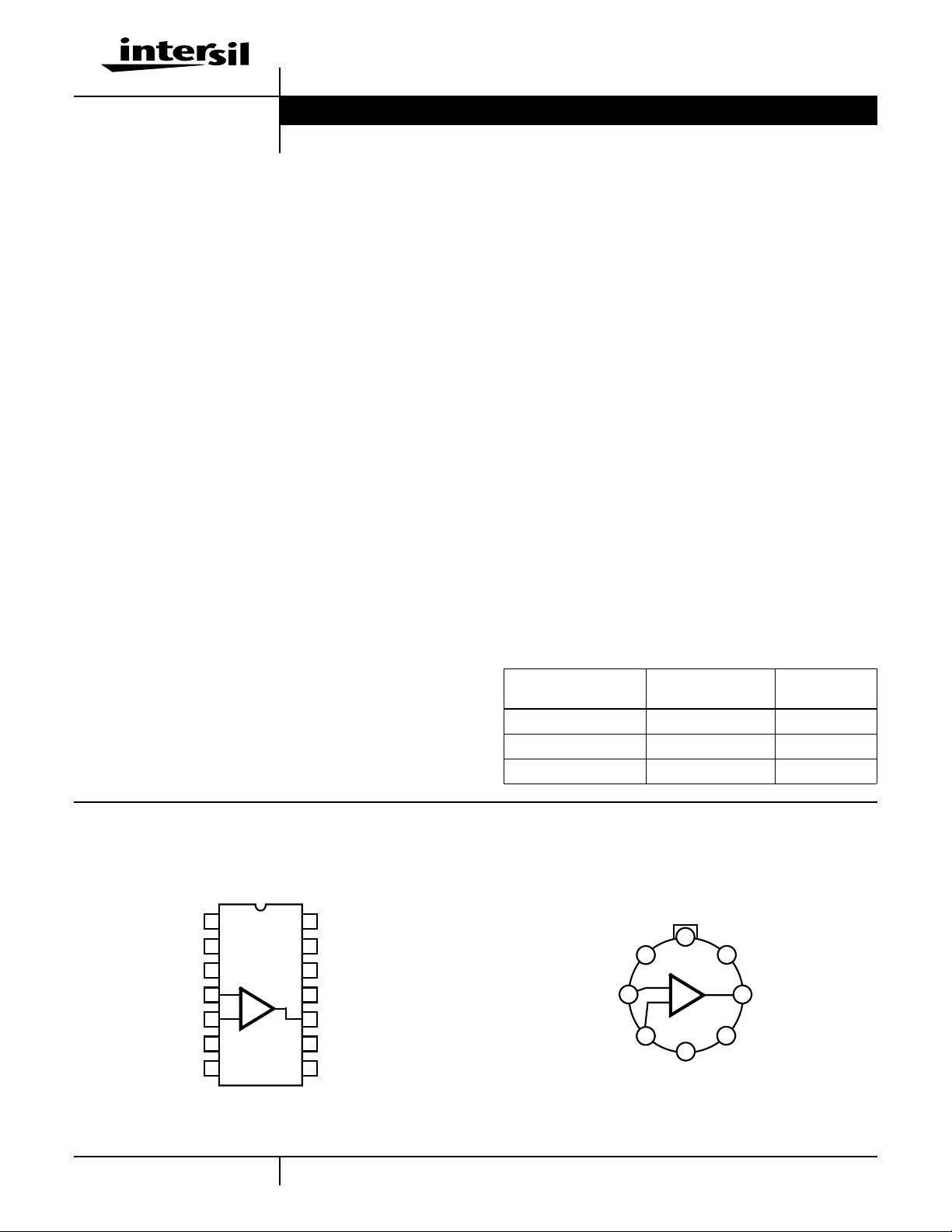
Pinouts
HS1-2700RH (CERDIP) GDIP1-T14
OR
HS1B-2700RH (SBDIP) CDIP2-T14
TOP VIEW
NC
BAL
GUARD
IN-
IN+
GUARD
1
2
3
4
-
+
5
6
7
V-
14
13
12
11
10
9
8
NC
NC
BAL
V+
OUTPUT
NC
NC
1
HS2-2700RH (CAN) MACY1-X8
TOP VIEW
BAL
8
BAL
1
2
IN-
IN+
CAUTION: These devices are sensitive to electrostatic discharge; follow proper IC Handling Procedures.
1-888-INTERSIL or 321-724-7143 | Copyright © Intersil Corporation 1999
-
+
3
7
V+
OUT
6
5
NC
4
V-
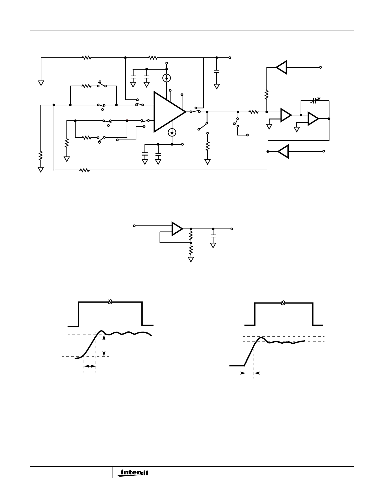
Test Circuit
HS-2700RH
400
10K
OPEN 2
10K
100
100
50K
2
S1
OPEN 2
2
1
OPEN
1 OPEN
S3A
S2
NOTE: Includes stray capacitances.
Timing Waveforms
1
S3B
1
VAC
VIN
1.6K
10.1
2
S5A
1
S6
1
2
-
DUT
+
10.1
+VCC
+
-
S5B
OPEN 1
-VEE
2
1
S8
2
2K
1.6K
ACOUT
75pF (NOTE)
OPEN
1
VOUT
75pF
S9
2
500K
V2
-1/10
FOR LOOP STABILITY,
USE MIN VALUE CAPACITOR
TO PREVENT OSCILLATION
50K
-1
-
+
BUFFER
2x
ALL RESISTORS = ±1% (Ω)
ALL CAPACITORS = ±10% (µF)
V1
-
+
E
OUT
400
FIGURE 1. SIMPLIFIED TEST CIRCUIT
INPUT
OUTPUT
-4V
-1.0V
+4V
+1.0V
+2.5V
-2.5V
∆T
∆V
OUTPUT
SLEW
RATE
= ∆V/∆T
INPUT
+160mV
0V
+40mV
0V
OVERSHOOT
90%
10%
RISE TIME
FIGURE 2. SLEW RATE WAVEFORM FIGURE 3. TRANSIENT RESPONSE WAVEFORM
NOTE: Measured on both positive and negative transitions. Capacitance at Compensation pin should be minimized.
0V
-40mV
2

HS-2700RH
Typical Performance Curves T
5
4
3
2
1
0
-1
VOLTAGE (mV)
-2
-3
-4
-5
-55 -25 0 25 50 75 100 125
TEMPERATURE (
= 25oC, VSUPPLY = ±15V, Unless Otherwise Specified
A
o
C)
FIGURE 4. OFFSETVOLTAGEAS A FUNCTION OF
TEMPERATURE
500
400
300
200
100
0
-100
-200
BIAS CURRENT (nA)
-300
-400
-500
-20 -15 -10 -5 0 5 10 15
COMMON MODE VOLTAGE (V)
VS = ±15.0V
T
= 25oC
A
30
20
10
0
CURRENT (mA)
-10
-20
-55 -25 0 25 50 75 100 125
TEMPERATURE (
BIAS CURRENT
OFFSET CURRENT
o
C)
FIGURE 5. INPUTBIAS CURRENT AND OFFSETCURRENT
AS A FUNCTION OF TEMPERATURE
10
9
8
7
6
5
4
3
BIAS CURRENT (µA)
2
1
0
20
0
5
DIFFERENTIAL INPUT VOLTAGE (V)
10
VS = ±15.0V
TA = 25oC
15
20
25
FIGURE 6. BIASCURRENT AS A FUNCTION OF COMMON
MODE VOLTAGE
1000
900
800
700
600
500
400
300
200
POWER SUPPLY CURRENT (µA)
100
0
0 100 200 300 400
DIFFERENTIAL INPUT VOLTAGE (mV)
VS = ±15.0V
= 25oC
T
A
500
FIGURE 8. POWER SUPPLY CURRENT ASA FUNCTION OF
DIFFERENTIAL INPUT VOLTAGE
3
FIGURE 7. BIASCURRENT AS A FUNCTIONOF
DIFFERENTIAL INPUT VOLTAGE
150
VS = ±20.0V
25
VS = ±15.0V
VS = ±10.0V
VS = ±5.5V
50
75
o
C)
100
125
120
90
60
30
POWER SUPPLY CURRENT (µA)
0
-55
-25
0
TEMPERATURE (
FIGURE 9. POWER SUPPLY CURRENT ASA FUNCTION OF
TEMPERATURE

HS-2700RH
Typical Performance Curves T
= 25oC, VSUPPLY = ±15V, Unless Otherwise Specified (Continued)
A
130
120
110
100
GAIN (dB)
VS = ±20.0V
90
80
-55 -25 0 25 50
VS = ±15.0V
VS = ±10.0V
VS = ±5.5V
TEMPERATURE (
o
C)
10075 125
FIGURE 10. VOLTAGE GAIN AS A FUNCTION OF TEMPERATURE
NOTE: Open loop (comparator) applications are not recommended, because of the above characteristic.
Burn-In Circuits
HS1-2700RH CERDIP
HS2-2700RH METAL CAN
V+
NC
1
2
NC
3
NC
4
5
6
NC
V-
D1C1
7
R1
14
NC
13
NC
12
NC
11
10
9
NC
8
NC
NOTES:
1. R1 = 1MΩ, ±5%, 1/4W (Min)
2. C1 = C2 = 0.01µF/Socket (Min) or 0.1µF/Row (Min)
3. D1 = D2 = 1N4002 or equivalent (per board)
4. |(V+) - (V-)| = 31V ±1V
D2
C2
V+
C2
D1
2
-
6
+
478
3
R1
V-
D2
C3
C1
NOTES:
5. R1 = 1MΩ, ±5%, 1/4W (Min)
6. C1 = 0.01µF/Socket (Min)
7. C2 = C3 = 0.01µF/Socket (Min) or 0.1µF/Row (Min)
8. D1 = D2 = 1N4002 or equivalent (per board)
9. |(V+) - (V-)| = 31V ±1V
10. Insulated scope probe must be used during board check-out.
4

HS-2700RH
Irradiation Circuit
NC
1
2
NC
3
NC
4
5
6
NC
V2
GND
7
R1
Schematic Diagram
V-
1
430K
Ω
14
NC
13
NC
12
NC
11
10
9
NC
8
NC
OS- OS+
NOTES:
11. R = 1MΩ, ±5%, 1/4W
12. V1 = +15V + 1.0V
13. V2 = -15V + 1.0V
V1
15Ω
IN+
2
V+
4
NOTE: Nominal currents shown in microamperes.
IN-
V+
15Ω
6
OUT
3
5

Die Characteristics
HS-2700RH
DIE DIMENSIONS:
70 mils x 60 mils x 20 mils
(1780µm x 1530µm x 1530µm)
INTERFACE MATERIALS:
Glassivation:
Type: Nitride
Thickness: 7k
Å ±0.7kÅ
Top Metallization:
Type: Aluminum
Thickness: 16k
Å ±2kÅ
Substrate:
Linear Bipolar, DI
Backside Finish:
Silicon
Metallization Mask Layout
ASSEMBLY RELATED INFORMATION:
Substrate Potential (Powered Up):
Unbiased
ADDITIONAL INFORMATION:
Worst Case Current Density:
< 2 x 10
HS-2700RH
+IN -IN
5
A/cm
2
V-
BAL
BAL
V+
OUTPUT
All Intersil semiconductor products are manufactured, assembled and tested under ISO9000 quality systems certification.
Intersil semiconductor products are sold by description only. Intersil Corporation reserves the right to make changesin circuit design and/or specifications at any time without notice. Accordingly, the reader is cautioned to verify that data sheets are current before placing orders. Information furnished by Intersil is believed to be accurate and
reliable. However, no responsibility is assumed by Intersil or its subsidiaries for its use; nor for any infringements of patents or other rights of third parties which may result
from its use. No license is granted by implication or otherwise under any patent or patent rights of Intersil or its subsidiaries.
For information regarding Intersil Corporation and its products, see web site http://www.intersil.com
6
 Loading...