

Page 1

HYNIX SEMICONDUCTOR
8-BIT SINGLE-CHIP MICROCONTROLLERS
HMS81004E
HMS81008E
HMS81016E
HMS81024E
HMS81032E
User’s Manual
(Ver. 1.00)
Page 2

Version 1.00
Published by
SP MCU Application Team
2001 Hynix Semiconductor, Inc. All right reserved.
Additional information of this manual may be served by Hynix Semiconductor offices in Korea or Distributors and Representatives listed at address directory.
Hynix Semiconductor reserves the right to make changes to any information here in at any time without notice.
The information, diagrams and other data in this manual are correct and reliable; however, Hynix Semiconductor is in no
way responsible for any violations of patents or other rights of the third party generated by the use of this manual.
Page 3

HMS81004E/08E/16E/24E/32E
Table of Contents
1. OVERVIEW ...........................................1
Description .........................................................1
Features .............................................................1
Development Tools ............................................ 2
2. BLOCK DIAGRAM ..............................3
3. PIN ASSIGNMENT (Top View) ........... 4
4. PACKAGE DIMENSION .......................5
5. PIN FUNCTION .....................................8
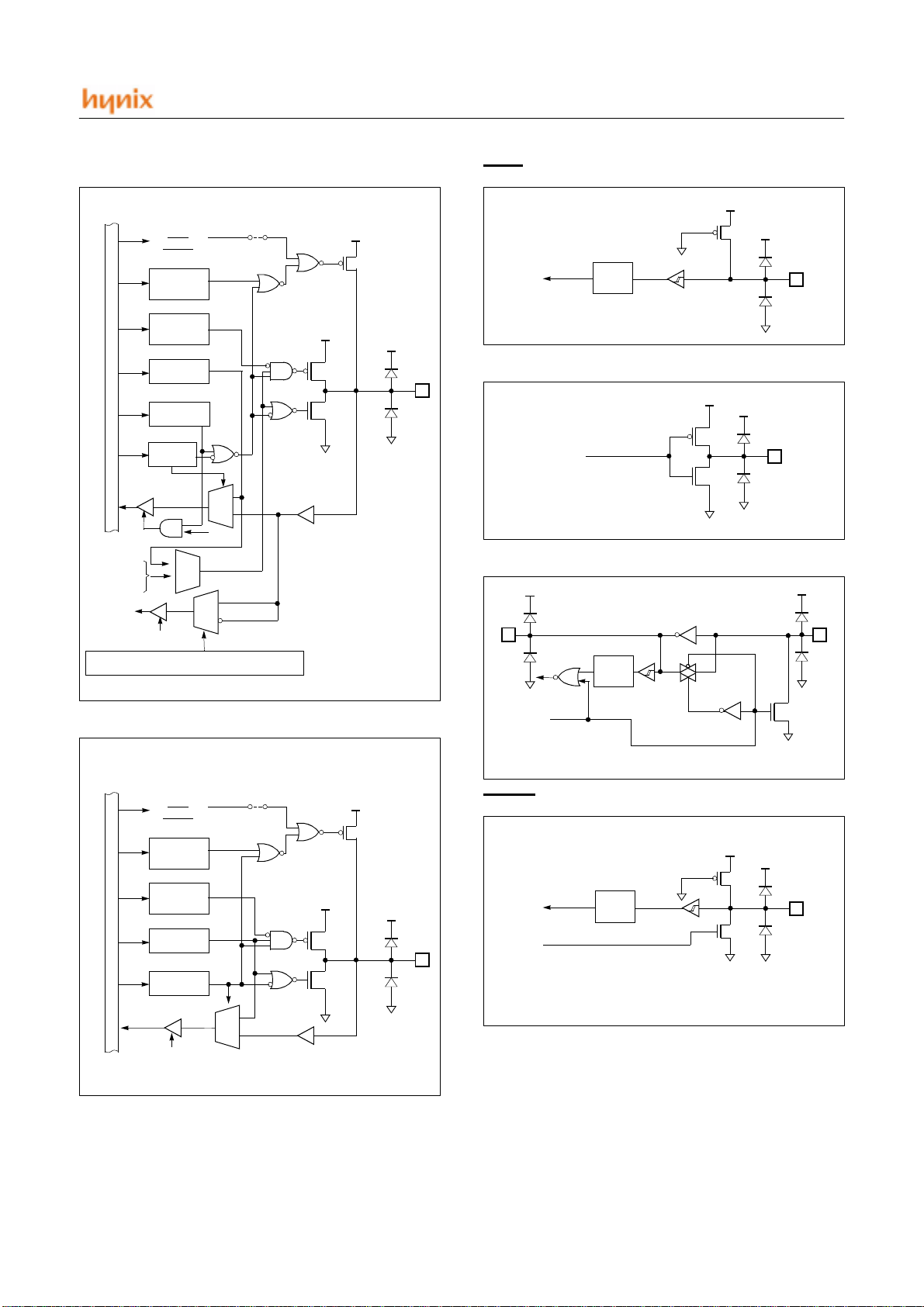
6. PORT STRUCTURES .........................10
7. ELECTRICAL CHARACTERISTICS ...12
Absolute Maximum Ratings .............................12
Recommended Operating Conditions ..............12
DC Electrical Characteristics ............................12
REMOUT Port Ioh Characteristics Graph ........13
REMOUT Port Iol Characteristics Graph .........14
AC Characteristics ...........................................14
8. MEMORY ORGANIZATION ................16
Registers ..........................................................16
Program Memory .............................................19
Data Memory ....................................................22
List for Control Registers.................................. 23
Addressing Mode .............................................25
9. I/O PORTS ..........................................30
R0 Ports........................................................... 30
R1 Ports ...........................................................30
R2 Port .............................................................32
10. CLOCK GENERATOR ......................33
Oscillation Circuit .......................................... 34
11. BASIC INTERVAL TIMER ................36
12. WATCH DOG TIMER .......................38
13. Timer0, Timer1, Timer2 ....................39
14. INTERRUPTS ...................................47
Interrupt priority and sources ........................ 48
Interrupt control register ................................ 48
Interrupt accept mode ................................... 49
Interrupt Sequence ........................................ 50
BRK Interrupt ................................................ 52
Multi Interrupt ................................................ 52
External Interrupt ........................................... 52
Key Scan Input Processing ........................... 53
15.STANDBY FUNCTION ......................55
Sleep Mode.................................................... 55
STOP MODE .................................................. 55
STANDBY MODE RELEASE ......................... 56
RELEASE OPERATION OF STANDBYMODE58
16. RESET FUNCTION ..........................60
EXTERNAL RESET ...................................... 60
POWER ON RESET ..................................... 60
Low Voltage Detection Mode ........................ 62
A. MASK ORDER SHEET ........................i
B. INSTRUCTION ....................................ii
Terminology List ...............................................ii
Instruction Map .................................................iii
Instruction Set ..................................................iv
JUNE 2001 Ver 1.00
Page 4
HMS81004E/08E/16E/24E/32E
HMS81004E/08E/16E/24E/32E
CMOS SINGLE- CHIP 8-BIT MICROCONTROLLER
FOR UNIVERSAL REMOTE CONTROLLER
1. OVERVIEW
1.1 Description
The HMS81004E/08E/16E/24E/32E is an advanced CMOS 8-bit microcontroller with 4/8/16/24/32K bytes of ROM. The
device is one of GMS800 family. The HYNIX HMS81004 E/08E/16E/24E/32E is a powerfu l microcontroller which provides
a highly flexible and cost effective solution to many UR applications.The HMS81004E/0 8E/16E/24E/32E provides the following standard features: 4/8/16/24/32K bytes of ROM, 448 bytes of RAM, 8-bit timer/counter, on-chip oscillator and clock
circuitry. In addition, the HMS81004E/08E/16E/24E/32E supports power saving modes to reduce power consumption.
Device Name ROM Size EPROM Size RAM Size Package
HMS81004E 4K Bytes HMS81008E 8K Bytes HMS81016E 16K Bytes HMS81024E 24K Bytes -
HMS81032E 32K Bytes HMS81020TL - 20K Bytes
HMS81032TL - 32K Bytes
1.2 Features
• Instruction Cycle Time:
- 1us at 4MHz
• Programmable I/O pins
20 PIN 24 PIN 28 PIN
INPUT 3 3 3
OUTPUT 2 2 2
I/O 13 17 21
• Operating Voltage
- 2.0 ~ 3.6 V @ 4MHz (MASK)
- 2.0 ~ 4.0 V @ 4MHZ (OTP)
•Timer
- Timer / Counter ......... 16Bit * 1ch
......... 8Bit * 2ch
- Basic Interval Timer ...... 8Bit * 1ch
448 Bytes
( included
256 bytes
stack memory )
- Watch Dog Timer ............ 6Bit * 1ch
• 8 Interrupt sources
- Nested Interrupt control is available.
- External input: 2
- Keyscan input
- Basic Interval Timer
- Watchdog timer
- Timer : 3
• Power On Reset
• Power saving Operation Modes
- STOP Operation
- SLEEP Operation
• Low Voltage Detection Circuit
• Watch Dog Timer Auto Start (During 1second
after Power on Reset)
20 SOP/PDIP
24 SOP/Skinny DIP
28 SOP/Skinny DIP
JUNE 2001 Ver 1.00 1
Page 5

HMS81004E/08E/16E/24E/32E
1.3 Development Tools
The HMS81004E/08E/16E/24E/32E are supported by a full-featured macro assembler, an in-circuit emulator CHOICE-Dr.
and OTP programmers. Macro assembler operates under the MSWindows 95/98
Please contact sales part of HYNIX
TM
/NT4/W2000.
TM
Software
Hardware
(Emulator)
OTP program-
mer
- MS- Window base assembler
- Linker / Editor / Debugger
- CHOICE-Dr.
- CHOICE-Dr. EVA 81C5EVA
- Universal single programmer.
- 4 gang programmer
- stand alone
2 JUNE 2001 Ver 1.00
Page 6
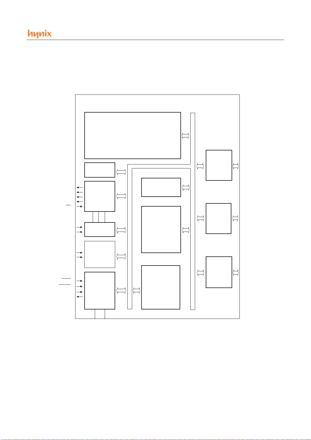
2. BLOCK DIAGRAM
HMS81004E/08E/16E/24E/32E
G8MC
Core
REMOUT
R17/T0
R16/T1
R15/T2
R14/EC
R12/INT2
R11/INT1
R00~R07
R10~R17
TEST
RESET
XIN
XOUT
Watchdog
Timer
Timer
Interrupt
Key Scan
INT.
Generation
Block
Clock Gen.
&
System
Control
RAM
(448byte)
ROM
(32kbyte)
Prescaler
&
B.I.T
R0
PORT
R1
PORT
R2
PORT
R00~R07
R10~R17
R20~R24
VDD VSS
JUNE 2001 Ver 1.00 3
Page 7
HMS81004E/08E/16E/24E/32E
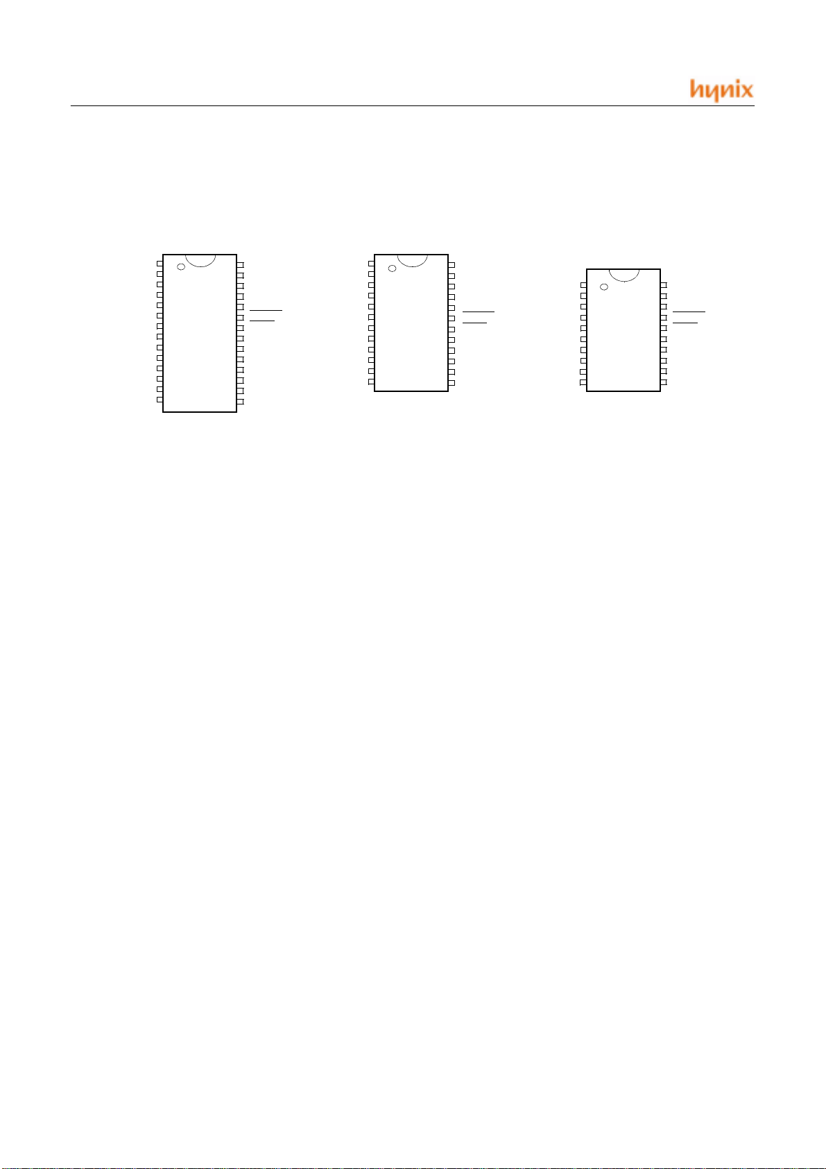
3. PIN ASSIGNMENT (Top View)
R13
R12
R11
R10
VDD
XOUT
XIN
R00
R01
R02
R03
R20
R21
R22
1
2
3
4
5
6
7
8
9
10
11
12
13
14
28PIN
28
27
26
25
24
23
22
21
20
19
18
17
16
15
R14
R15
R16
R17
REMOUT
RESET
TEST
R07
R06
R05
R04
VSS
R24
R23
R13
R12
R11
R10
VDD
XOUT
XIN
R00
R01
R02
R03
R20
1
2
3
4
5
6
7
8
9
10
11
12
24PIN
24
23
22
21
20
19
18
17
16
15
14
13
R14
R15
R16
R17
REMOUT
RESET
TEST
R07
R06
R05
R04
VSS
R11
R10
VDD
XOUT
XIN
R00
R01
R02
R03
R20
1
2
3
4
5
6
7
8
9
10
20PIN
20
19
18
17
16
15
14
13
12
11
R16
R17
REMOUT
RESET
TEST
R07
R06
R05
R04
VSS
4 JUNE 2001 Ver 1.00
Page 8
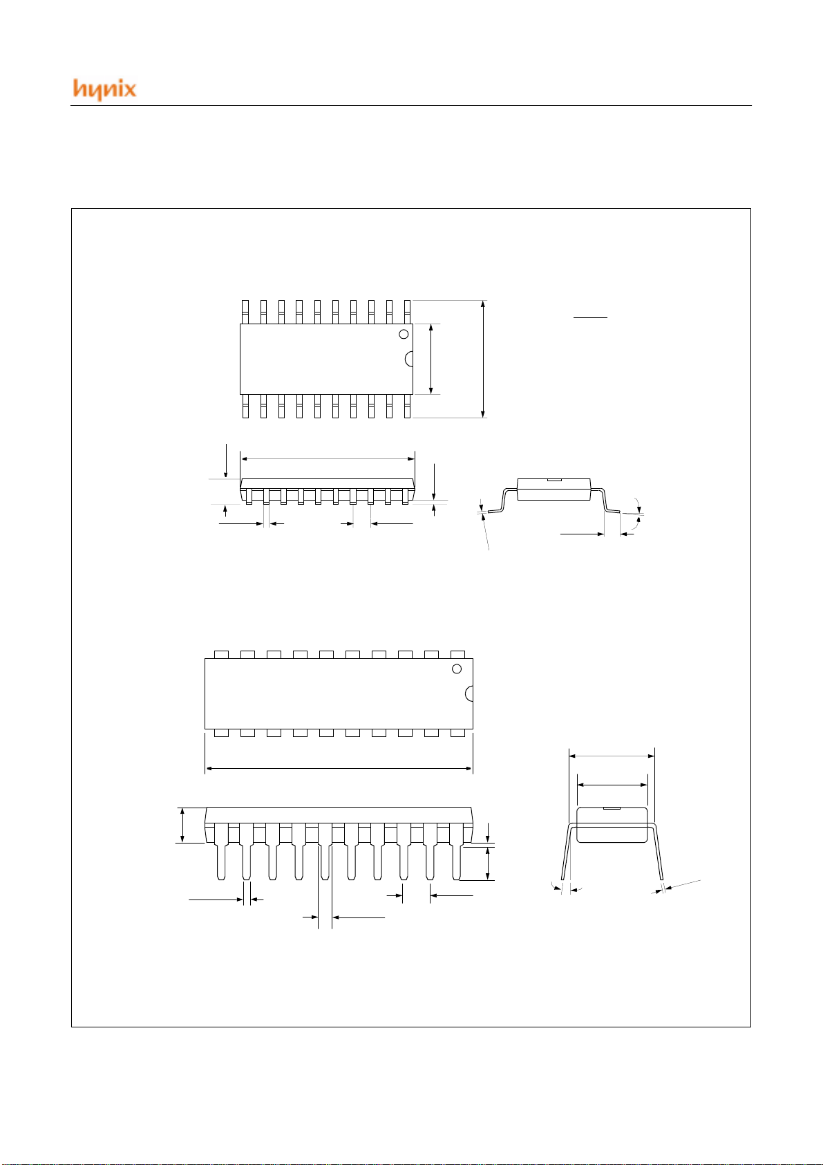
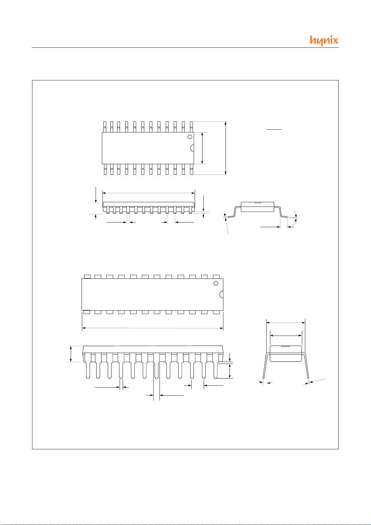
4. PACKAGE DIMENSION
HMS81004E/08E/16E/24E/32E
20 SOP
20 PDIP
0.093
0.105
0.020
0.013
0.512
0.495
0.050 BSC
0.229
0.291
0.012
0.004
0.419
3
1
0
.
0
0.398
8
0
0
.
0
UNIT: INCH
MAX
MIN
0.042
0.016
0 ~ 8°
0 ~ 15°
0.300 BSC
0.270
0.245
012
0.
08
0
0.
MAX 0.180
0.021
0.015
1.043
1.015
0.065
0.050
0.100 BSC
MIN 0.015
0.120
0.140
JUNE 2001 Ver 1.00 5
Page 9
HMS81004E/08E/16E/24E/32E
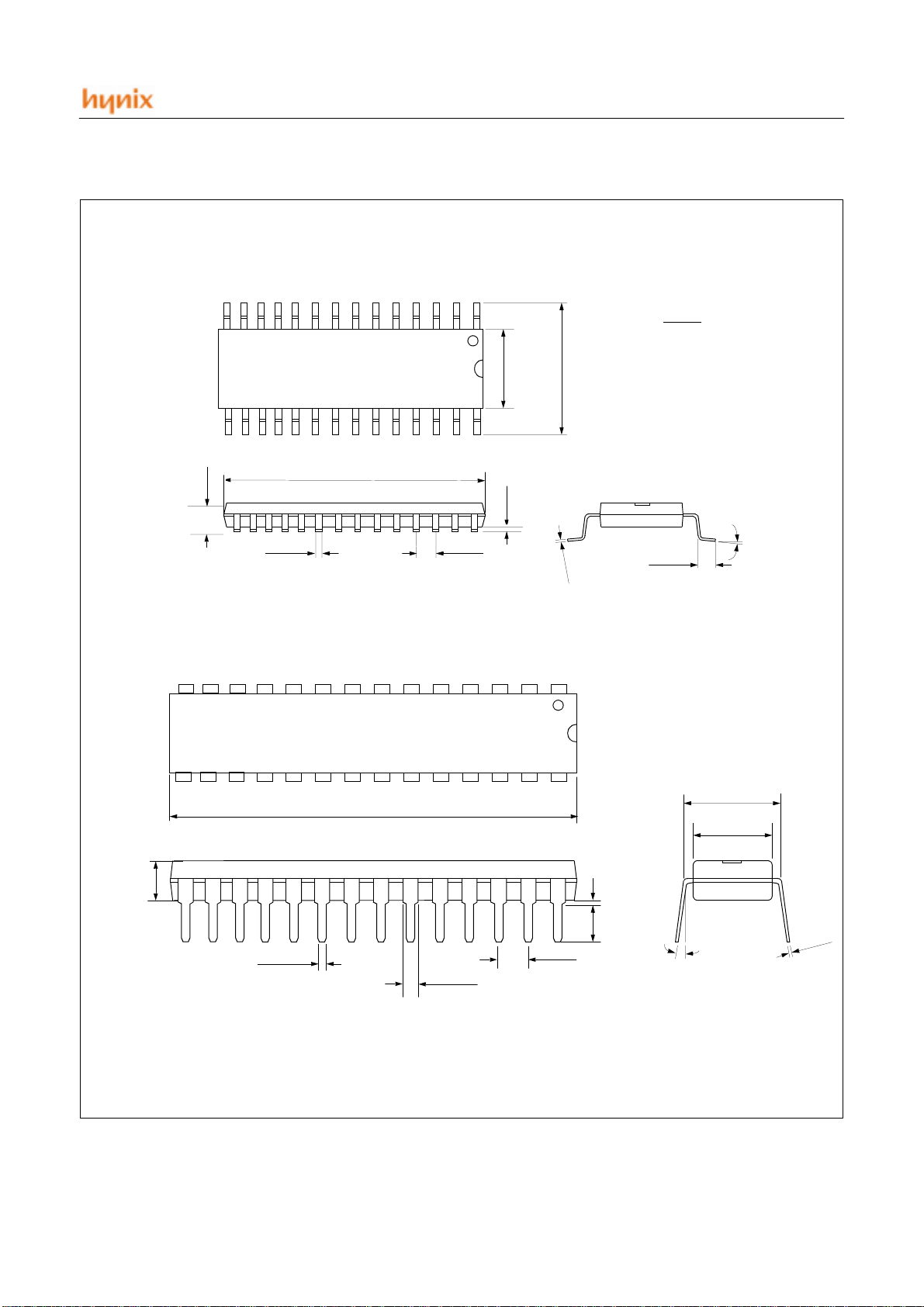
24 SOP
24 SKDIP
0.093
0.106
0.020
0.013
0.614
0.598
0.050 BSC
0.229
0.291
0.004
0.012
UNIT: INCH
MAX
MIN
0.419
0.398
8
3
0
1
0
.
0
.
0
0
0.042
0.016
0 ~ 8°
0 ~ 15°
0.300 BSC
0.300
0.250
14
0
0.
008
0.
MAX 0.180
0.021
0.015
1.265
1.160
0.065
0.045
0.100 BSC
MIN 0.015
0.120
0.140
6 JUNE 2001 Ver 1.00
Page 10
HMS81004E/08E/16E/24E/32E
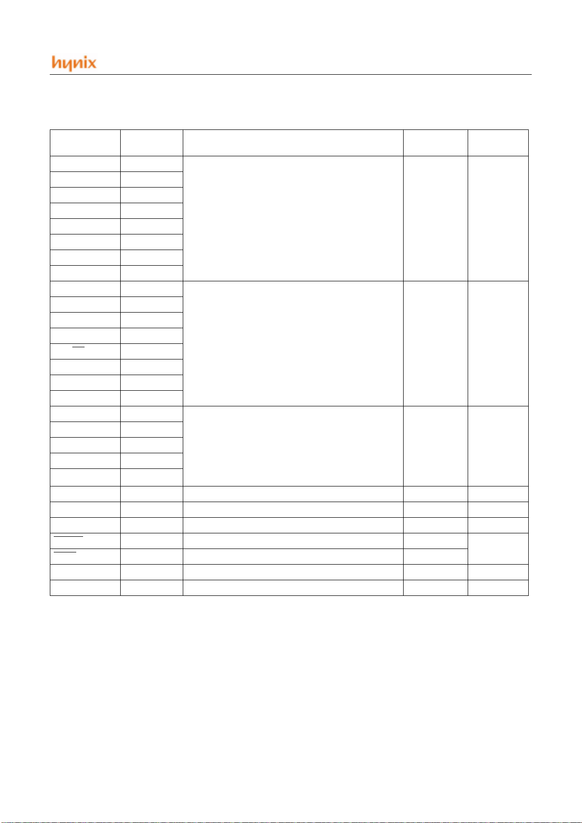
28 SOP
UNIT: INCH
MAX
MIN
0.229
0.291
0.419
0.398
0.713
0.093
0.106
0.697
0.004
0.012
MAX 0.180
28 SKDIP
0.020
0.013
0.021
0.015
1.375
1.355
0.050 BSC
0.055
0.045
8
3
0
1
0
.
0
.
0
0
0.100 BSC
MIN 0.015
0.120
0.140
0.042
0.016
0 ~ 15°
0 ~ 8°
0.300 BSC
0.300
0.275
14
0
0.
008
0.
JUNE 2001 Ver 1.00 7
Page 11

HMS81004E/08E/16E/24E/32E
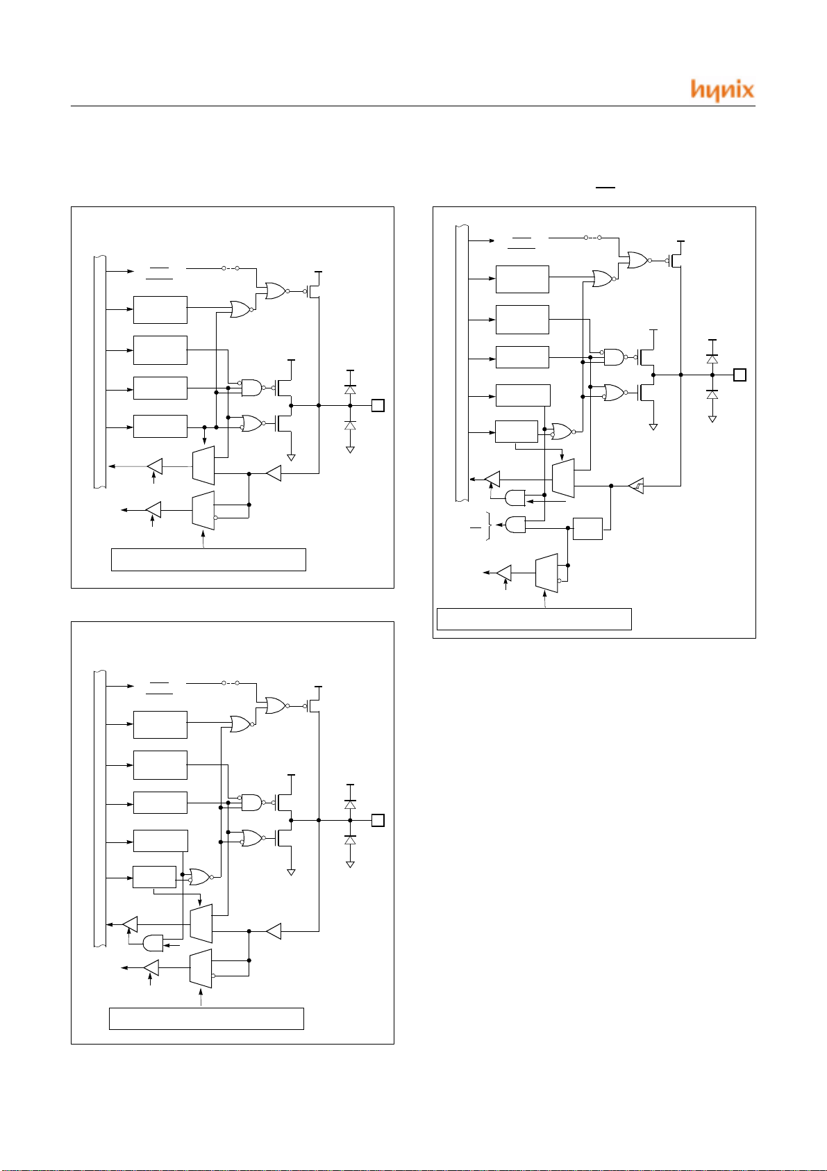
5. PIN FUNCTION
V
: Supply voltage.
DD
V
: Circuit ground.
SS
TEST
: Used for shipping inspection of the IC. For normal
operation, it should be connected to V
RESET
X
: Reset the MCU.
: Input to the inverting oscillator amplifier and input to
IN
DD
.
the internal main clock operating circuit.
X
: Output from the inverting oscillator amplifier.
OUT
R00~R07
: R0 is an 8-bit CMOS bidirectional I/O port. R0
pins 1 or 0 written to the Port Direction Register can be
used as output s or inputs.
R10~R17
: R1 is an 8-bit CMOS bidirectional I/O port. R1
pins 1 or 0 written to the Port Direction Register can be
used as outputs or inputs.
In addition, R1 serves the functions of the various follow -
ing special features .
Port pin Alternate function
R11
R12
R14
R15
R16
R17
R20~R24
INT1 (External Interrupt input 1)
INT2 (External Interrupt input 2)
EC
T2 (Timer / Counter input 2)
T1 (Timer / Counter input 1)
T0 (Timer / Counter input 0)
: R2 is an 8-bit CMOS bidirectional I/O port. R2
(Event Counter input )
pins 1 or 0 written to the Port Direction Register can be
used as outputs or inputs .
8 JUNE 2001 Ver 1.00
Page 12
HMS81004E/08E/16E/24E/32E
PIN NAME
R00 I/O
R01 I/O
R02 I/O
R03 I/O
R04 I/O
R05 I/O
R06 I/O
R07 I/O
R10 I/O
R11/INT1 I/O
R12/INT2 I/O
R13 I/O
R14/EC
R15/T2 I/O
R16/T1 I/O
R17/T0 I/O
R20 I/O - Each bit of the port can be individually configured as
R21 I/O
R22 I/O
R23 I/O
R24 I/O
XIN I Oscillator input Low
XOUT O Oscillator output High
REMOUT O High current output ‘L’ output ‘L’ output
RESET
TEST
VDD P Positive power supply
VSS P Groud
INPUT/
OUTPUT
- Each bit of the port can be individually configured as
an input or an output by user software
- Push-pull output
- CMOS input with pull-up resister (option)
- Can be programmable as key scan input
- Pull-up resisters are automatically disabled at output
mode
- Each bit of the port can be individually configured as
an input or an output by user software
- Push-pull output
- CMOS input with pull-up resister (option)
I/O
I Includes pull-up resistor ‘L’ level
I Includes pull-up resistor
- Can be programmable as key scan input or open
drain output
- Pull-up resisters are automatically disabled at output
mode
- Direct driving of LED(N-Tr.)
an input or an output by user software
- Push-pull output
- CMOS input with pull-up resister (option)
- Pull-up resisters are automatically disabled at output
mode
- Direct driving of LED(N-Tr.)
Function @RESET @STOP
INPUT
INPUT
INPUT
State of
before
Stop
State of
before
Stop
State of
before
Stop
state of
before stop
JUNE 2001 Ver 1.00 9
Page 13
HMS81004E/08E/16E/24E/32E
Pin
Data Reg.
Function Sele-
Key Scan
Pull up
Reg.
Rd
V
DD
V
SS
Pull-up Tr.
Input
Open Drain
Reg.
Data Bus
Tr.: Transistor
Reg.: Register
LVD
Circuit
OTP : connected
MASK : option (default connected)
V
DD
KS_EN
Standby Release Level Control Regist er
ction Reg.
Dir Reg.
MUX
Noise
Filter
to R11...INT1
to R12...INT2
to R14...EC
MUX
6. PORT STRUCTURES
R0[0:7]
Data Bus
Key Scan
Input
OTP : connected
LVD
Circuit
Pull up
Reg.
Open Drain
Reg.
Data Reg.
Dir. Reg.
Rd
KS_EN
Standby Release Level Control Register
MASK : option (default connected)
V
DD
V
SS
MUX
MUX
V
DD
Pull-up Tr.
Tr.: Transistor
Reg.: Register
R11/INT1, R12/INT2, R14/EC
Pin
R10, R13
Data Bus
Key Scan
Input
OTP : connected
LVD
Circuit
Pull up
Reg.
Open Drain
Reg.
Data Reg.
Function Selection Reg.
Dir Reg.
KS_EN
Standby Release Level Control Register
MASK : option (default connected)
V
DD
Rd
MUX
MUX
V
SS
V
DD
Pull-up Tr.
Tr.: Transistor
Reg.: Register
Pin
10 JUNE 2001 Ver 1.00
Page 14
HMS81004E/08E/16E/24E/32E
Pin
V
DD
V
SS
Noise
Filter
Pin
V
DD
V
SS
Internal Signal
XIN
V
SS
XOUT
Noise
Filter
from STOP circuit
Pin
V
DD
V
SS
Noise
Filter
from Power On Reset
R15/T2, R16/T1, R17/T0
OTP : connected
LVD
Circuit
Pull up
Reg.
Open Drain
Reg.
Data Reg.
Data Bus
Function Selection Reg.
Dir Reg.
to R15...T2
to R16...T1
to R17...T0
Key Scan
Input
Standby Release Level Control Register
KS_EN
MASK : option (default connected)
MUX
Rd
MUX
MUX
TEST
V
DD
Pull-up Tr.
V
DD
REMOUT
Pin
V
SS
XIN, XOUT
Tr.: Transistor
Reg.: Register
R2[0:4]
OTP : connected
LVD
Circuit
Pull up
Reg.
Open Drain
Reg.
Data Reg.
Data Bus
Dir. Reg.
Rd
JUNE 2001 Ver 1.00 11
MASK : option (default connected)
MUX
V
DD
Pull-up Tr.
V
DD
Pin
V
SS
Tr.: Transistor
Reg.: Register
RESET
Page 15
HMS81004E/08E/16E/24E/32E
7. ELECTRICAL CHARACTERISTICS
7.1 Absolute Maximum Ratings
Supply voltage...........................................-0.3 to +5.0 V
Input Voltage .....................................-0.3 to V
Output Voltage ...................................-0.3 to V
DD
DD
+0.3 V
+0.3 V
Operating Temperature........................................ 0~70°C
Storage Temperature ......................................-65~150°C
Power Dissipation................................................700 mA
7.2 Recommended Operating Conditions
Parameter Symbol Condition
Supply Voltage
Operating Frequency
Operating Temperature
V
T
DD
f
XIN
OPR
f
XIN
VDD=2.0~3.6V
7.3 DC Electrical Characteristics
(TA=-0~70°C, VDD=2.0~3.6V, GND=0V)
Parameter Symbol Condition
Note: Stresses above those listed under “Absolute Maxi-
mum Ratings” may cause per manent damage to the d evice. This is a stress ra ting only and functional ope r ati on of
the device at any oth er c ond iti ons ab ov e tho se ind ic ated in
the oper ati o na l se c ti ons of this s pe c ifi ca t io n i s no t i m pl ie d .
Exposure to absolute maximum rating conditions for extended periods may affect device reliability.
Specifications
Unit
Min. Max.
=4MHz
2.0 3.6 V
1.0 4.0 MHz
-0+70
°
C
Specifications
Unit
Min. Typ. Max.
High level
input Voltage
Low level
input Voltage
Hign level input
Leakage Current
Low level input
Leakage Current
High level
output Voltage
Low level
output Voltage
Hign level output
Leakage Current
Low level output
Leakage Current
V
V
V
V
V
V
V
V
V
V
I
I
IH1
IH2
IL1
IL2
I
IH
I
IL
OH1
OH2
OH3
OL1
OL2
OL3
OHL
OLL
R11,R12,R14,RESET
R0,R1(except R11,R12,R14), R2
R11,R12,R14,RESET 0R0,R1(except R11,R12,R14), R2 0 -
R0,R1,R2,RESET ,VIH= VDD
R0,R1,R2,RESET (without pu ll-up),VIL= 0
R0, IOH=-0.5mA
R1[6:0], R2, IOH=-1.0mA
XIN, XOUT,IOH=-200µA
R0, IOL=1mA
R1, R2, IOL=5mA
XIN, XOUT,IOL=200µA
R0,R1,R2, VOH= VDD
R0,R1,R2, VOL= 0
0.8 V
0.7 V
DD
DD
-
-
0.2 V
0.3 V
--1µA
---1µA
VDD-0.4 - - V
VDD-0.4 - - V
VDD-0.9 - - V
--0.4V
--0.8V
--0.8V
--1µA
---1µA
V
DD
V
DD
DD
DD
V
V
V
V
12 JUNE 2001 Ver 1.00
Page 16
HMS81004E/08E/16E/24E/32E
Parameter Symbol Condition
High Level
output current
Low Level
output cruuent
Input pul l-up curren t
Power Supply Current
RAM retention
supply voltage
I
OH
I
OL
I
I
DD1
I
DD2
I
SLP1
I
SLP2
I
STP1
I
STP2
V
RET
REMOUT, R17, V
REMOUT, V
R0,R1,R2, RESET, VDD=3V 15 30 60
p
Operating current ,fxin=4Mhz, VDD=2.0V - 2.4 6 mA
Operating current ,fxin=4Mhz, VDD=3.6V - 4 10 mA
Sleep mode current ,fxin=4Mhz,
VDD=2.0V
Sleep mode current ,fxin=4Mhz,
VDD=3.6V
Stop mode current ,Oscillator Stop
VDD=2.0V
Stop mode current ,Oscillator Stop
VDD=3.6V
OL
Specifications
Unit
Min. Typ. Max.
=2V -30
OH
=1V
0.5 - 3 mA
-12 -5 mA
µ
A
-12mA
-23mA
-28µA
-310µA
-0.7--V
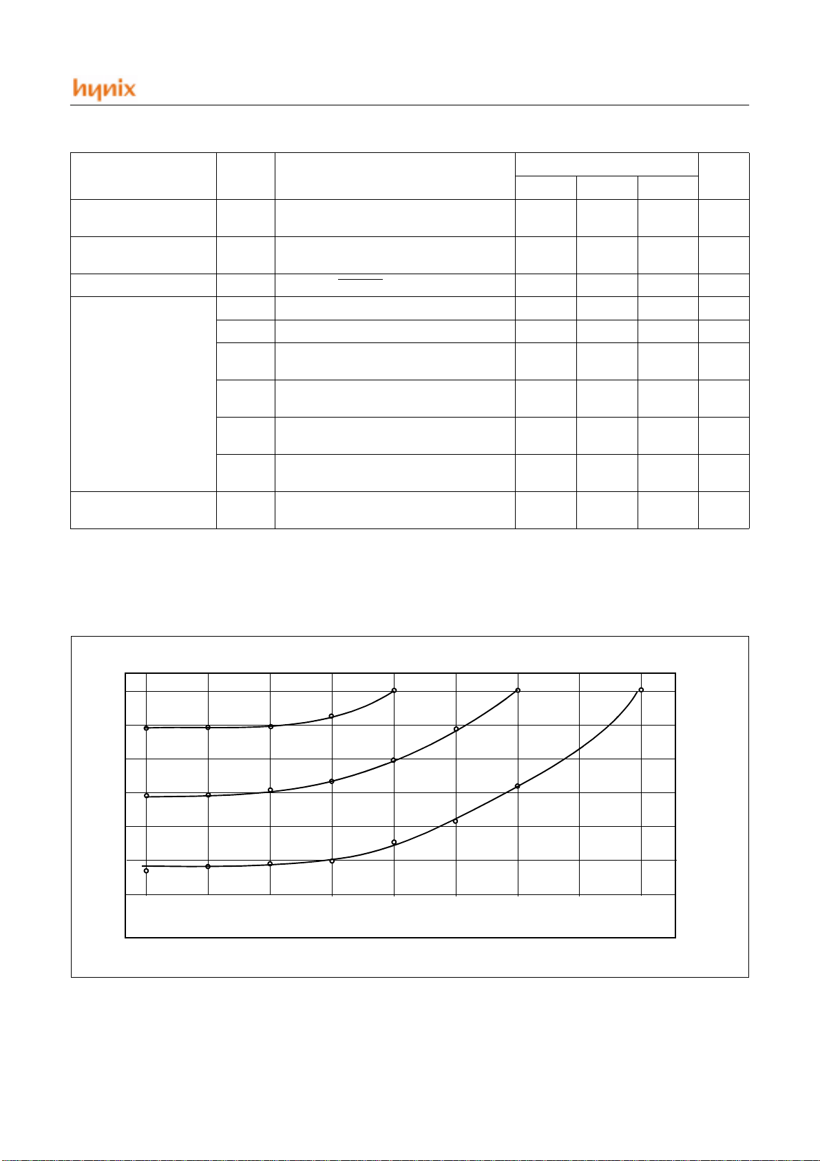
7.4 REMOUT Port Ioh Characteristics Graph
(typical process & room temperature)
.
Ioh(mA)
0
-5
-10
-15
-20
-25
-30
0 0.5 1.0 1.5 2.0 2.5 3.0 3.5 4.0
Voh (
Vdd 2V
Vdd 3V
Vdd 4V
V)
Figure 7-1 Ioh vs Voh
JUNE 2001 Ver 1.00 13
Page 17
HMS81004E/08E/16E/24E/32E
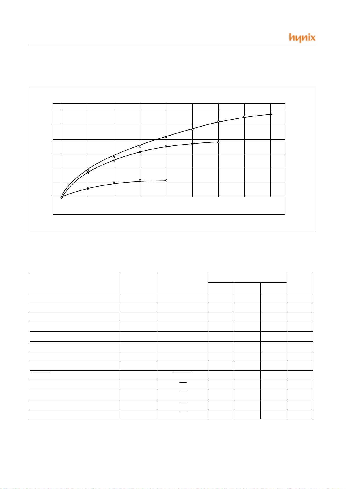
7.5 REMOUT Port Iol Characteristics Graph
(typical process & room temperature)
.
Iol(mA)
5
4
3
2
1
0
-1
0 0.5 1.0 1.5 2.0 2.5 3.0 3.5 4.0
7.6 AC Characteristics
(TA=0~+70°°°°C, VDD=2.0~3.6V, VSS=0V)
Parameter Symbol Pins
Vdd 2V
Vol (
V)
Figure 7-2 Iol vs Vol
Vdd 4V
Vdd 3V
Specifications
Unit
Min. Typ. Max.
External clock input cycle time
System clock cycle time
External clock pulse width High
External clock pulse width Low
External clock rising time
External clock falling time
Interrupt pulse width High
Interrupt pulse width Low
RESET Input pulse width low
Event counter input pulse width high
Event counter input pulse width low
Event counter input pulse rising time
Event counter input pu lse fa lling time
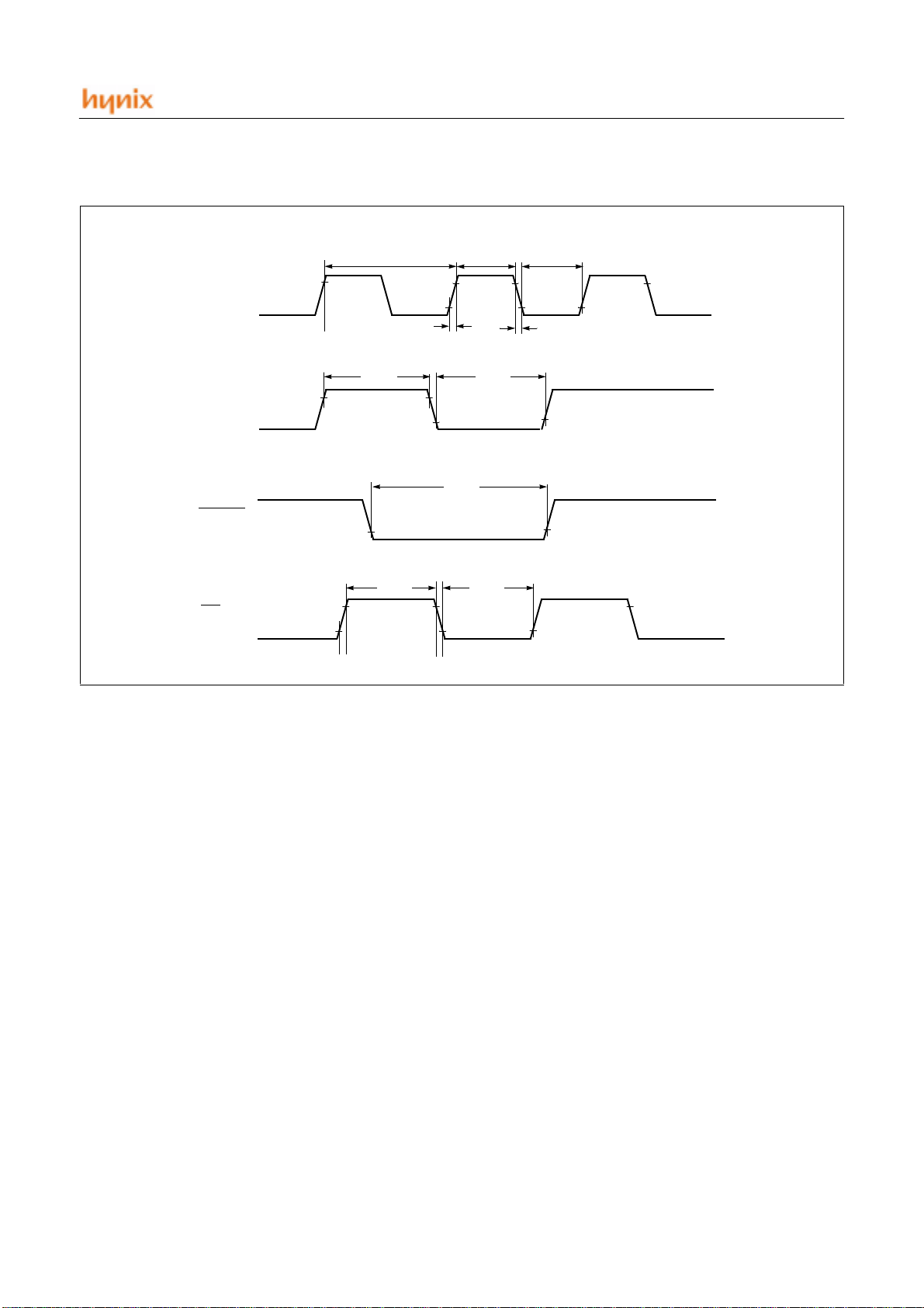
t
CP
t
SYS
t
CPH
t
CPL
t
RCP
t
FCP
t
t
t
RSTL
t
ECH
t
ECL
t
REC
t
FEC
IH
IL
X
IN
250 500 1000 ns
500 1000 2000
X
IN
X
IN
X
IN
X
IN
40 - - ns
40 - - ns
- - 40 ns
- - 40 nS
INT1, INT2 2 - INT1, INT2 2 - -
RESET 8--
EC 2-EC 2-EC --40
EC --40
t
SYS
t
SYS
t
SYS
t
SYS
t
SYS
ns
ns
ns
14 JUNE 2001 Ver 1.00
Page 18
HMS81004E/08E/16E/24E/32E
X
IN
INT1
INT2
RESET
EC
t
CP
t
RCP
t
IH
0.8V
DD
t
RSTL
t
ECH
Figure 7-3 Timing Diagram
t
CPH
t
ECL
t
CPL
-0.5V
V
DD
0.5V
t
FCP
t
IL
0.2V
DD
0.2V
DD
0.8V
DD
0.2V
DD
JUNE 2001 Ver 1.00 15
Page 19
HMS81004E/08E/16E/24E/32E
8. MEMORY ORGANIZATION
The HMS81004E/08E/16E/24E/32E has separate address
spaces for Program memory and Data Memory. Program
memory can only be read, not written to. It can be up to
8.1 Registers
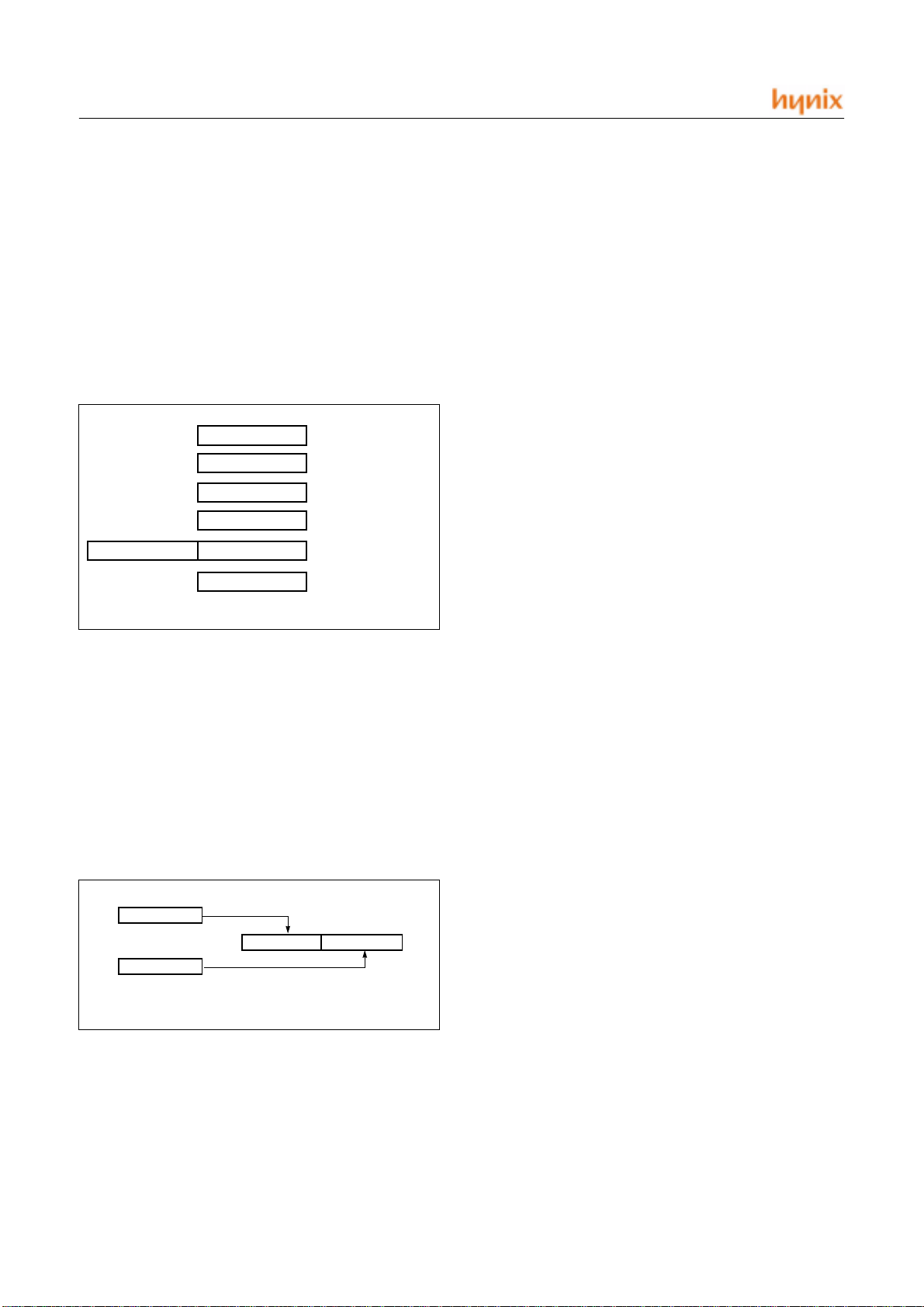
This device has six registers that are the Program Counter
(PC), an Accumulator (A), two index registers (X, Y), the
Stack Pointer (SP), and the Program Status Word (PSW).
The Program Counter consists of 16-bit register.
A
X
Y
SP
PCLPCH
PSW
Figure 8-1 Configuration of Registers
Accumulator:
The Accumulator is the 8-bit general purpose register, used
for data operation such as transfer, temporary saving, and
conditional judgement, etc. The Accumulator can be used
as a 16-bit register with Y Register as shown below.
In the case of multiplication instruction, execute as a multiplier register. After multiplication operation, the lower 8bit of the result enters. (Y*A => YA). In the case of division instruction, ex ecute as the lo wer 8-bit of di vidend. After division operation, quotient enters.
Y
A
Two 8-bit Registers can be used as a "YA" 16-bit Register
ACCUMULATOR
X REGISTER
Y REGISTER
STACK POINTER
PROGRAM COUNTER
PROGRAM STATUS
WORD
Y A
32K bytes of Program memory. Data memory can be read
and written to up to 448 bytes including the stack area.
X, Y Registers:
In the addressing mode which uses these index registers,
the register contents are added to the specified address,
which becomes the actual address. These modes are extremely effective for referencing subroutine tables and
memory tables. The index registers also have increment,
decrement, comparison and data transfer functions, and
they can be used as simple accumulators.
• X Regist er
In the case of division instruction, execute as register.
• Y Regist er
In the case of 16-bit operation instruction, execute as the
upper 8-bit of YA. (16-bit accumulator). In the case of
multiplication instruction, execute as a multiplicand register. After multiplication operation, the upper 8-bit of the
result enters. In the case of division instruction, execute as
the upper 8-bit of dividend. After division operation, remains enters. Y register can be used as loop counter of
conditional branch command. (e.g.DBNE Y, rel)
Stack Pointer:
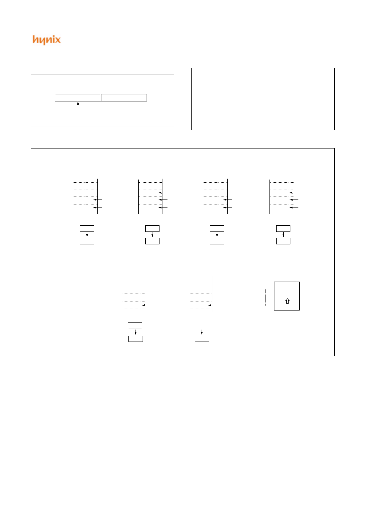
The Stack Pointer is an 8-bit register used for occurrence
interrupts, calling out subroutines and P USH, POP, RETI,
RET instruction. Stack Pointer identifies the location in the
stack to be accessed (save or restore).
Generally, SP is automatically updated when a subrout ine
call is executed or an interrupt is accepted. However, if it
is used in excess of the stack area permitted by the data
memory allocating configuration, the user-processed data
may be lost. The SP is post-decremented when a subroutine call or a push instruction is executed, or when an interrupt is accepted. The SP is pre-incremented when a return
or a pop instruction is executed.
Figure 8-2 Configuration of YA 16-bit Register
The stack can be located at any position within 100
1FF
of the internal data memory. The SP is not initialized
H
to
H
by hardware, requiring to write the initial v alue (the lo cation with which the use of the stack starts) by using the initialization routine. Normally, the initial value of "FF
H
" is
16 JUNE 2001 Ver 1.00
Page 20
HMS81004E/08E/16E/24E/32E
used.
Stack Address ( 100H ~ 1FFH )
15 087
01
H
Hardware fixed
At execution of
a CALL/TCALL/PCALL
01FC
01FD
01FE
01FF
SP before
execution
SP after
execution
PCL
PCH
01FF
01FD
Push
down
SP
01FC
01FD
01FE
01FF
At acceptance
of interrupt
PSW
PCL
PCH
01FF
01FC
Push
down
Caution:
The Stack Pointer must be initialized by software be-
cause its value is undefined after RESET.
Example: To initialize the SP
LDX #0FFH
TXSP ; SP ← FFH
At execution
of RET instruction
01FC
01FD
01FE
01FF
PCL
PCH
01FD
01FF
Pop
up
At execution
of RETI instruction
01FC
01FD
01FE
01FF
PSW
PCL
PCH
01FC
01FF
Pop
up
At execution
of PUSH instruction
PUSH A (X,Y,PSW)
01FC
01FD
SP before
execution
SP after
execution
01FE
01FF
01FF
01FE
Push
A
down
Figure 8-3 Stack Operation
Program Counter:
The Program Counter is a 16-bit wide which consists of
two 8-bit registers, PCH and PCL. This counter indicates
the address of the next instruction to be executed. In reset
state, the program counter has reset routine address
(PC
:0FFH, PCL:0FEH).
H
Program Status Word:
The Program Status Word (PSW) contains several bits that
At execution
of POP instruction
POP A (X,Y,PSW)
01FC
01FD
01FE
01FF
A
01FE
01FF
Pop
up
0100H
01FFH
Stack
depth
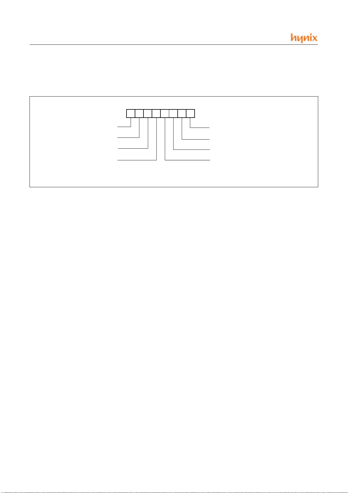
reflect the current state of the CPU. The PSW is described
in Figure 8-4 . It contains the Negative flag, the Overflow
flag, the Break flag the Half Carry (for BCD operation),
the Interrupt enable flag, the Zero flag, and the Carry flag.
[Carry flag C]
This flag stores any carry or borrow from the ALU of CPU
after an arithmetic operation and is also changed by the
Shift Instruction or Rotate Instruction.
JUNE 2001 Ver 1.00 17
Page 21
HMS81004E/08E/16E/24E/32E
[Zero flag Z]
This flag is set when the result of an arithmetic operat ion
or data transfer is "0" and is cleared by any other result.
MSB LSB
N
PSW
V G B H I Z C
RESET VALUE : 00
H
NEGATIVE FLAG
OVERFLOW FLAG
SELECT DIRECT PAGE
when g=1, page is addressed by RPR
BRK FLAG
Figure 8-4 PSW (Program Status Word) Register
[Interrupt disable flag I]
This flag enables/disables all interrupts except interrupt
caused by Reset or software BRK instruction. All interrupts are disabled when cleared to "0". This flag immediately becomes "0" when an interrupt is served. It is set by
the EI instruction and cleared by the DI instruction.
[Half carry flag H]
After operation, this is set when there is a carry from bit 3
of ALU or there is no borrow from bit 4 of ALU. This bit
can not be set or cleared except CLRV instruction with
Overflow flag (V).
[Break flag B]
This flag is set by software BRK instruction to distinguish
BRK from TCALL instruction with the same vector address.
[Direct page flag G]
CARRY FLAG RECEIVES
CARRY OUT
ZERO FLAG
INTERRUPT ENABLE FLAG
HALF CARRY FLAG RECEIVES
CARRY OUT FROM BIT 1 OF
ADDITION OPERLANDS
the direct addressing mode, addressing area is from zero
page 00
to 0FFH when this flag is "0". If it is set to "1",
H
addressing area is 1 Page. It is set by SETG instruction and
cleared by CLRG.
[Overflow flag V]
This flag is set to "1" when an overflow occurs as the result
of an arithmetic operation involving signs. An overflow
occurs when the result of an addition or subtraction exceeds +127(7F
) or -128(80H). The CLRV instruction
H
clears the overflow flag. There is no set instruction. When
the BIT instruction is executed, bit 6 of memory is copied
to this flag.
[Negative flag N]
This flag is set to match the sign bit (bit 7) status of the result of a data or arithmetic operation. When the BIT instruction is executed, bit 7 of memory is copied to this flag.
This flag assigns RAM page for di rect addressing mode. I n
18 JUNE 2001 Ver 1.00
Page 22
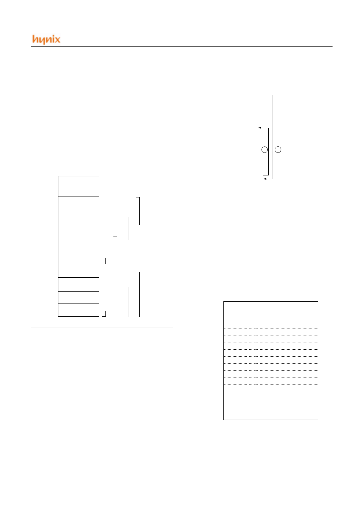
8.2 Program Memory
E0
E2
Address
Vector Area Memory
E4
E6
E8
EA
EC
EE
F0
F2
F4
F6
F8
FA
FC
FE
-
-
-
Basic Interval Timer Interrupt Vector Area
-
-
Timer2 Interrupt Vector Area
Timer0 Interrupt Vector Area
-
External Interrupt 2 Vector Area
Key Scan Interrupt Vector Area
RESET Vector Area
External Interrupt 1 Vector Area
Timer1 Interrupt Vector Area
Watch Dog Timer Interrupt Vector Area
"-" means reserved area.
NOTE:
-
0FFDE
H
S/W Interrupt Vector Area
HMS81004E/08E/16E/24E/32E
A 16-bit program counter is capable of addressing up to
64K bytes, but this device has 4/8/16/24/32K bytes program memory space only physically implemented. Accessing a location above FFFF
to 0000
.
H
will cause a wrap-around
H
Figure 8-5 , shows a map of Progr am Memory. After reset,
the CPU begins execution from reset vector which is stored
in address FFFE
and FFFFH as shown in Figure 8-6 .
H
As shown in Figure 8-5 , each area is assigned a fixed location in Program M emory. Program Memory area contains the user program.
8000
H
A000
H
C000
H
32KROM
E000
F000
FF00
FFC0
FFE0
FFFF
H
H
H
H
H
INTERRUPT
VECTOR AREA
H
PCALL
AREA
TCALL
AREA
8KROM
4KROM
HMS81008E
HMS81004E
KROM
HMS81016E 16
24KROM
HMS81032E
HMS81024E
Example: Usage of TCALL
LDA #5
TCALL 0FH ;
:;
:;
;
;TABLE CALL ROUTINE
;
FUNC_A: LDA LRG0
RET
;
FUNC_B: LDA LRG1
RET
;
;TABLE CALL ADD. AREA
;
ORG 0FFC0H ;
DW FUNC_A
DW FUNC_B
1BYTE INSTRUCTION
IN STEAD OF 2 BYTES
NORMAL CALL
1
2
TCALL ADDRESS AREA
The interrupt causes the CPU to jum p to specific location,
where it commences the execution of the service routine.
The External interrupt 0, for example, is assigned to location 0FFFA
interval: 0FFF8
0FFFA
Any area from 0FF00
. The interrupt service locations spaces 2-byte
H
and 0FFF9H for External Interru pt 1,
H
and 0FFFBH for External Interrupt 0, etc.
H
to 0FFFFH, if it is not going to be
H
used, its service location is available as general purpose
Program Memory.
Figure 8-5 Program Memory Map
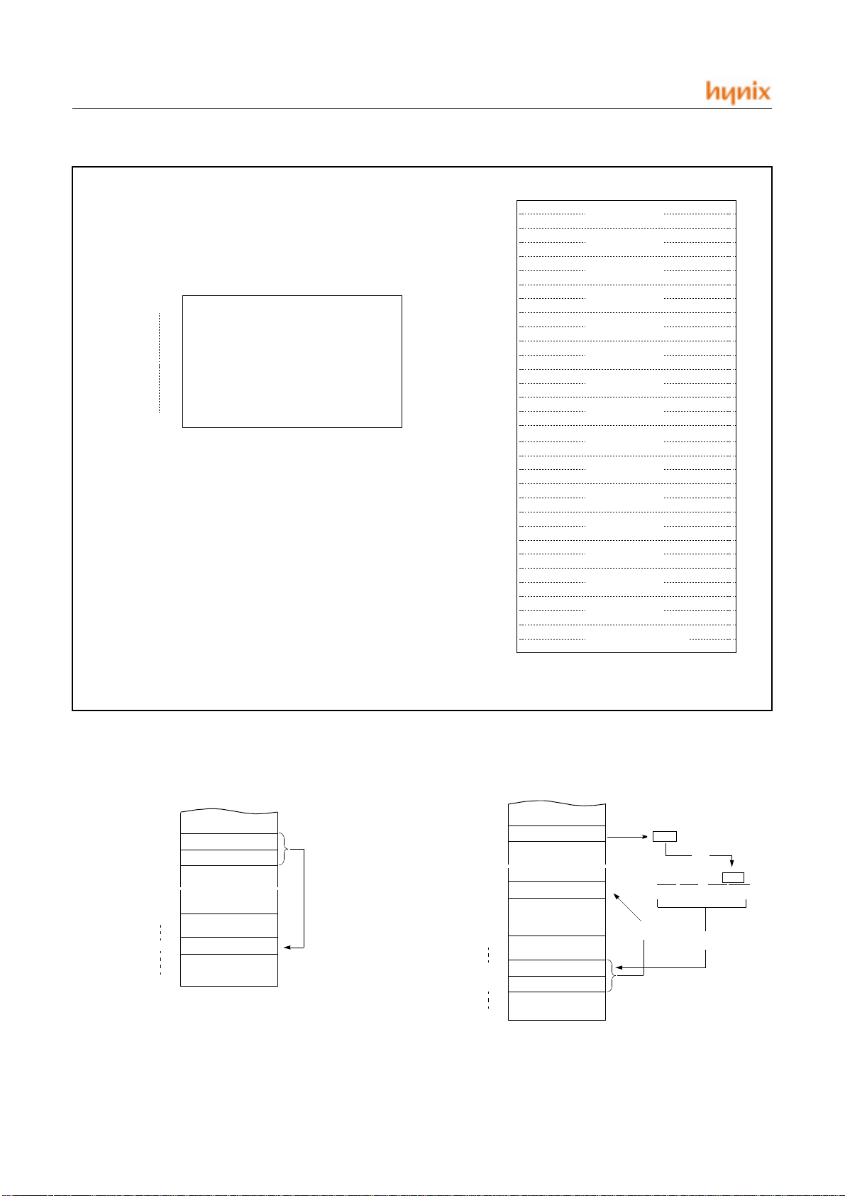
Page Call (PCALL) area contains subroutine program to
reduce program byte length by using 2 bytes PCALL instead of 3 bytes CALL instruction. If it is frequently
called, it is more useful to save program byte length.
Table Call (TCALL) c auses the CPU to jump to each
TCALL address, where it commences the execution of the
service routine. The Table Call service area spaces 2-byte
for every TCALL: 0FFC0
TCALL14, etc., as shown in Figure 8-7 .
JUNE 2001 Ver 1.00 19
for TCALL15, 0FFC2H for
H
Figure 8-6 Interrupt Vector Area
Page 23
HMS81004E/08E/16E/24E/32E
11111111
11010110
01001010
PC:
FHFHDH6
H
4A
~
~
~
~
25
0FFD6H
0FF00H
0FFFFH
D1
NEXT
0FFD7H
➊
➋
➌
0D125H
Reverse
Address PCALL Area Memory
0FF00
H
PCALL Area
(192 Bytes)
0FFBF
H
Address Pro gram Memory
0FFC0
H
C1
C2
C3
C4
C5
C6
C7
C8
C9
CA
CB
CC
CD
CE
CF
D0
D1
D2
D3
D4
D5
D6
D7
D8
D9
DA
DB
DC
DD
DE
DF
NOTE:
* means that the BRK software interrupt is using
same address with TCALL0.
TCALL 15
TCALL 14
TCALL 13
TCALL 12
TCALL 11
TCALL 10
TCALL 9
TCALL 8
TCALL 7
TCALL 6
TCALL 5
TCALL 4
TCALL 3
TCALL 2
TCALL 1
TCALL 0 / BRK *
Figure 8-7 PCALL and TCALL Memory Area
PCALL
4F35 PCALL 35H
20 JUNE 2001 Ver 1.00
→
→
→ →
rel
0FF00H
0FF35H
0FFFFH
TCALL
→
→
→ →
n
4A TCALL 4
4F
35
~
~
NEXT
~
~
Page 24

HMS81004E/08E/16E/24E/32E
Example: The usage software example of Vector address and the initialize part.
ORG 0FFE0H
DW NOT_USED
DW NOT_USED
DW NOT_USED
DW B IT_INT ; BIT
DW WDT_INT ; Watch Dog Timer
DW NOT_USED
DW NOT_USED
DW T MR2_INT ; Timer-2
DW T MR1_INT ; Timer-1
DW T MR0_INT ; Timer-0
DW N OT_USED ;
DW I NT2 ; Int.2
DW I NT1 ; Int.1
DW K EY_INT ; Key Scan
DW N OT_USED ;
DW R ESET ; Reset
ORG 08000H ;HMS81032E Program start address
;********************************************
; MAIN PROGRAM *
;********************************************
;
RESET: NOP
RAM_CLR: LDA #0 ;RAM Clear(!0000H->!00BFH)
CLRG
DI ;Disable All Interrupts
LDX #0
STA {X}+
CMPX #0C0H
BNE RAM_CLR ;
LDX #0FFH ;Stack Pointer Initialize
TXSP
LDM R0, #0 ;Normal Port 0
LDM R0DD,#1000_0010B ;Normal Port Direction
LDM P0PC,#1000_0010B ;Pull Up Selection Set
LDM PMR1,#0000_0010B ;R1 port / int
:
:
LDM CKCTLR,#0011_1101B ;WDT ON , 16mS Time delay after stop mode release
:
:
JUNE 2001 Ver 1.00 21
Page 25
HMS81004E/08E/16E/24E/32E
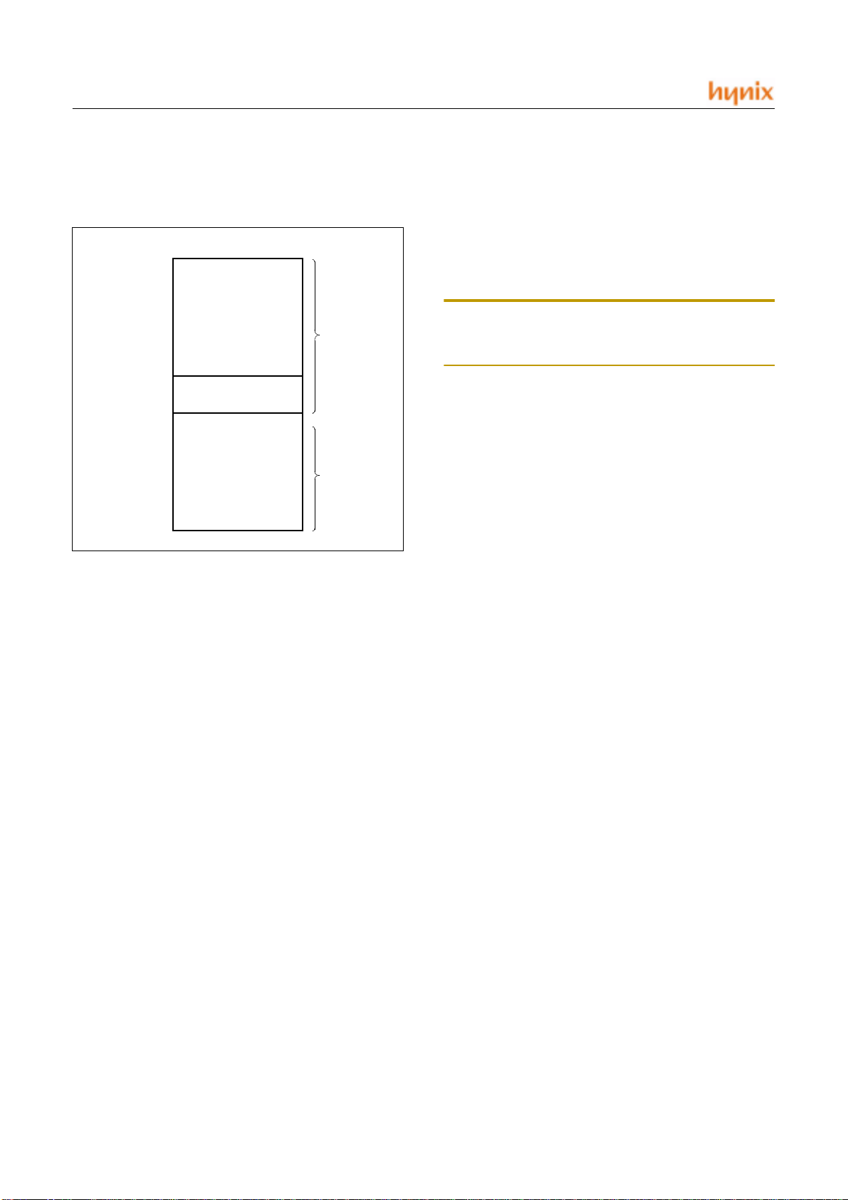
8.3 Data Memory
Figure 8-8 shows the internal Data Memory space available. Data Memory is divided into 3 groups, a user RAM,
control registers, Stack.
0000H
Note that unoccupied addresses may not be implemented
on the chip. Read accesses to these addresses will in general return random data, and write accesses will have an indeterminate effect.
More detailed informations of each register are explained
in each peripheral section.
RAM
(192 Bytes)
00BFH
00C0H
00FFH
0100H
01FFH
Figure 8-8 Data Memory Map
CONTROL
REGISTERS
RAM (STACK)
(256 Bytes)
PAGE0
PAGE1
User Memory
The HMS81004E/08E/16E/24E/32E has 448 × 8 bits for
the user memory (RAM).
Control Registers
The control registers are used by the CPU and Peripheral
function blocks for controlling the desired operation of the
device. Therefore these registers contain control and status
bits for the interrupt system, the timer/ counters, analog to
digital converters and I/O ports. The control registers are in
address range of 0C0
to 0FFH.
H
Note: Write only registers can not be accessed by bit manipulation instruction. Do not use read-modify-write instruction. Use byte manipulation instruction.
Example; To write at CKCTLR
LDM CLCTLR,#09H ;Divide ratio
÷16
Stack Area
The stack provides the area where the return address is
saved before a jump is performed during the processing
routine at the execution of a subroutine call instruction or
the acceptance of an interrupt.
When returning from the processing routine, execu ting the
subroutine return instruction [RET] restores the contents of
the program counter from the stack; ex ecuting the interrupt
return instruction [RETI] restores the contents of the program counter and flags.
The save/restore locations in the stack are determined by
the stack pointed (SP). The SP is automatically decreased
after the saving, and increased before the restoring. This
means the value of the SP indicates the stack location
number for t he next save. Refer to Figure 8-3 on page 17.
22 JUNE 2001 Ver 1.00
Page 26
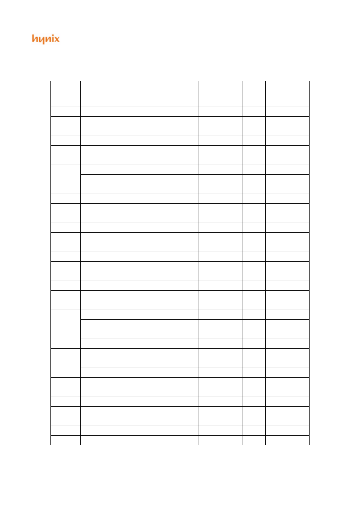
List for Control Registers
8.4
HMS81004E/08E/16E/24E/32E
Address Function Register Symbol
00C0h PORT R0 DATA REG. R0 R/W undefined
00C1h PORT R0 DATA DIRECTION REG. R0DD W 00000000b
00C2h PORT R1 DATA REG. R1 R/W undefined
00C3h PORT R1 DATA DIRECTION REG. R1DD W 00000000b
00C4h PORT R2 DATA REG. R2 R/W undefined
00C5h PORT R2 DATA DIRECTION REG. R2DD W 00000000b
00C6h reserved
00C7h
00C8h WATCH DOG TIMER REG. WDTR W -000 1111b
00C9h PORT R1 MODE REG. PMR1 W 00000000b
00CAh INT. MODE REG. IMOD R/W -0000000b
00CBh EXT. INT. EDGE SELECTION IEDS W 00000000b
00CCh INT. ENABLE REG. LOW IENL R/W -00-----b
00CDh INT. REQUEST FLAG REG. LOW IRQL R/W -00-----b
00CEh INT. ENABLE REG. HIGH IENH R/W 000-000-b
00CFh INT. REQUEST FLAG REG. HIGH IRQH R/W 000-000-b
00D0h TIMER0 (16bit) MODE REG. TM0 R/W 00000000b
00D1h TIMER1 (8bit) MODE REG. TM1 R/W 00000000b
00D2h TIMER2 (8bit) MODE REG. TM2 R/W 00000000b
00D3h TIMER0 HIGH-MSB DATA REG. T0HMD W undefined
00D4h TIMER0 HIGH-LSB DATA REG. T0HLD W undefined
00D5h
00D6h
00D7h TIMER1 HIGH DATA REG. T1HD W undefined
00D8h
00D9h
00DAh TIMER0 / TIMER1 MODE REG. TM01 R/W 00000000b
00DBh Reserved
00DCh STANDBY MODE RELEASE REG0 SMPR0 R/W 00000000b
00DDh STANDBY MODE RELEASE REG0 SMPR1 R/W 00000000b
00DEh PORT R1 OPEN DRAIN ASSIGN REG. R1ODC R/W 00000000b
CLOCK CONTROL REG. CKCTLR W --110111b
BASIC INTERVAL REG. BTR R undefined
TIMER0 LOW-MSB DATA REG. T0LMD W undefined
TIMER0 HIGH-MSB COUNT REG. R undefined
TIMER0 LOW-LSB DATA REG. T0LLD W undefined
TIMER0 LOW-LSB COUNT REG. W undefined
TIMER1 LOW DATA REG. T1LD W undefined
TIMER1 LOW COUNT REG. R undefined
TIMER2 DATA REG. T2DR W undefined
TIMER2 COUNT REG. R undefined
Read
Write
RESET Value
JUNE 2001 Ver 1.00 23
Page 27
HMS81004E/08E/16E/24E/32E
00DFh PO RT R2 OPEN DRAIN ASSIGN REG. R2ODC R/W 00000000b
00E0h Reserved
00E1h Reserved
00E2h Reserved
00E3h Reserved
00E4h PORT R0 OPEN DRAIN ASSIGN REG. R0ODC R/W 00000000b
00E5h Reserved
00E6h Reserved
00E7h Reserved
00E8h Reserved
00E9h Reserved
00EAh Reserved
00EBh Reserved
00ECh Reserved
00EDh Reserved
00EEh Reserved
00EFh Reserved
00F0h SLEEP MODE REG. SLPM W - - - - - - - 0b
00F1h Reserved
00F2 Reserved
00F3h Reserved
00F4h Reserved
00F5h Reserved
00F6h STANDBY RELEASE LEVEL CONT. REG. 0 SRLC0 W 00000000b
00F7h STANDBY RELEASE LEVEL CONT. REG. 1 SRLC1 W 00000000b
00F8h PORT R0 PULL-UP REG. CONT. REG. R0PC W 00000000b
00F9h PORT R1 PULL-UP REG. CONT. REG. R1PC W 00000000b
00FAh PORT R2 PULL-UP REG. CONT. REG. R2PC W 00000000b
00FBh Reserved
00FCh Reserved
00FDh Reserved
00FEh Reserved
00FFh Reserved
W
R/W
- : this bit location is reserved.
Registers are controlled by byte manipulation instruction such as LDM etc., do not use bit manipulation
instruction such as SET1, CLR1 etc. If bit manipulation instruction is used on these registers,
content of other seven bits are may varied to unwanted value.
Registers are controlled by both bit and byte manipulation instruction.
24 JUNE 2001 Ver 1.00
Page 28

8.5 Addressing Mode
E4
0F100
H
data
←
55H
~
~
~
~
data
0C35
H
➊
35
0F102
H
55
0F101
H
➋
data
35
35
H
0E551
H
data → A
➋
➊
~
~
~
~
C5
0E550
H
HMS81004E/08E/16E/24E/32E
The HMS81004E/08E /16E/24E/32E uses six addressing
modes;
• Register addressing
• Immediate addressing
• Direct page addressing
• Absolute addressing
• Indexed addressing
• Register-indirect addressing
(1) Register Addressing
Register addressing accesses the A, X, Y, C and PSW.
(2) Immediate Addressing
→
→
→ →
#imm
In this mode, second byte (operand) is accessed as a data
immediate ly.
Example:
0435 ADC #35H
E45535 LDM 35H,#55H
(3) Direct Page Addressing
→
→
→ →
dp
In this mode, a address is specified within direct page.
Example; G=0
C535 LDA 35H ;A ←RAM[35H]
MEMORY
04
35
A+35H+C → A
When G-flag is 1, then RAM address is difined by 16-bit
address which is composed of 8-bit RAM paging register
(RPR) and 8-bit immediate data.
Example: G=1, RPR=0CH
(4) Absolute Addressing
→
→
→ →
!abs
Absolute addressing sets corresponding memory data to
Data , i.e. second byte(Operand I) of command becomes
lower level address and third byte (Operand II) becomes
upper level address.
With 3 bytes command, it is possible to access to whole
memory area.
ADC, AND, CMP, CMPX, CMPY, EOR, LDA, LDX,
LDY, OR, SBC, STA, STX, STY
Example;
JUNE 2001 Ver 1.00 25
Page 29

HMS81004E/08E/16E/24E/32E
0735F0 ADC !0F035H ;A ←ROM[0F035H]
0F035
0F100
0F101
0F102
H
H
H
H
data
~
~
07
35
F0
~
~
➋
A+data+C → A
➊
address: 0F035
26 JUNE 2001 Ver 1.00
Page 30
HMS81004E/08E/16E/24E/32E
data
DB
35
H
data → A
➋
➊
~
~
~
~
36H → X
data
45
3A
H
0E551
H
data → A
➋
➊
~
~
~
~
C6
0E550
H
45H+0F5H=13AH
➌
The operation within data memory (RAM)
ASL, BIT, DEC, INC, LSR, ROL, ROR
Example; Addressing accesses the address 0135
regard-
H
less of G-flag and RPR.
983501 INC !0135H ;A ←ROM[135H]
135
0F100
0F101
0F102
H
H
H
H
data
~
~
98
35
01
~
~
➌
➋
data+1 → data
➊
address: 0135
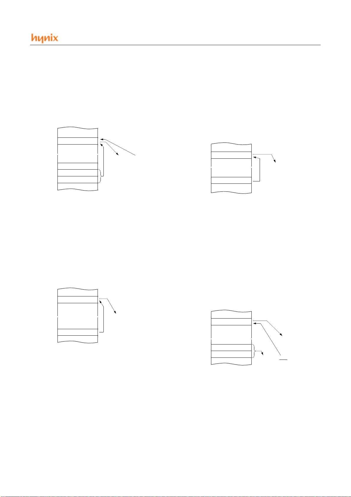
(5) Indexed Addressing
X indexed direct page (no offset)
→
→
→ →
{X}
In this mode, a address is specified by the X register.
ADC, AND, CMP, EOR, LDA, OR, SBC, STA, XMA
Example; X=15
D4 LDA {X} ;ACC←RAM[X].
115
H
H
, G=1, RPR=01
data
H
➋
X indexed direct page, auto increment
→
→
→ →
{X}+
In this mode, a address is specified within direct page by
the X register and the content of X is increased by 1.
LDA, STA
Example; G=0, X=35
DB LDA {X}+
X indexed direct page (8 bit offset)
H
dp+X
→
→
→ →
This address value is the second byte (Operand) of command plus the data of -register. And it assigns the memory in Direct page.
ADC, AND, CMP, EOR, LDA, LDY, OR, SBC, STA
STY, XMA, ASL, DEC, INC, LSR, ROL, ROR
Example; G=0, X=0F5
C645 LDA 45H+X
H
~
~
~
~
data → A
➊
0E550
H
JUNE 2001 Ver 1.00 27
D4
Page 31
HMS81004E/08E/16E/24E/32E
0A
35
H
jump to address 0E30A
H
➊
~
~
~
~
35
0FA00
H
E3
36
H
➋
3F
0E30A
H
NEXT
~
~
~
~
05
35
H
0E005
H
~
~
~
~
25
0FA00
H
E0
36
H
16
0E005
H
data
~
~
~
~
➌
A + data + C → A
25 + X(10) = 35
H
➊
➋
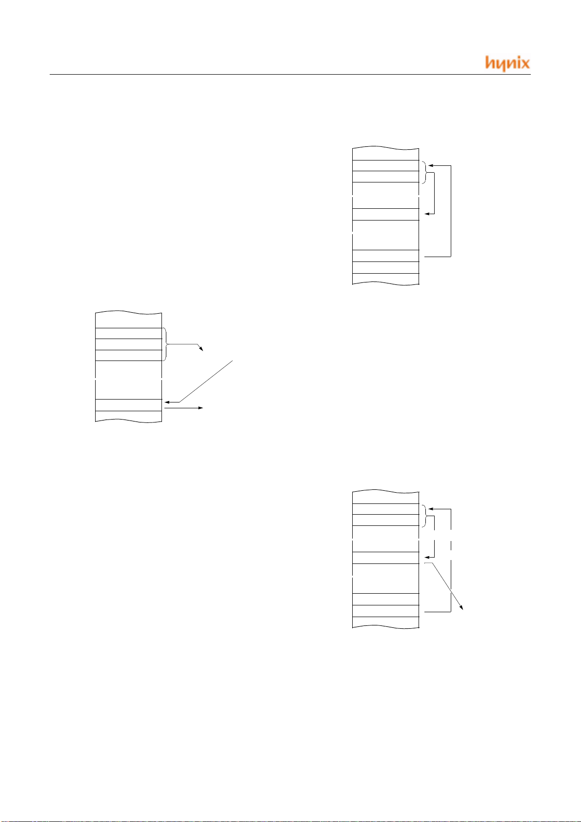
Y indexed direct page (8 bit offset)
→
→
→ →
dp+Y
This address value is the second byte (Operand) of command plus the data of Y- register, whic h assigns Memory in
Direct page.
This is same with above (2). Use Y register instead of X.
Y indexed absolute
!abs+Y
→
→
→ →
Sets the value of 16-bit absolute address plus Y-register
data as Memory. This addressing mode can specify memory in whole area.
Example; Y=55
D500FA LDA !0FA00H+Y
0F100
0F101
0F102
0FA55
H
H
H
H
~
~
H
D5
00
FA
data
➊
0FA00H+55H=0FA55H
~
~
➋
data → A
➌
3F35 JMP [35H]
X indexed indirect
→
→
→ →
[dp+X]
Processes memory data as Data, assigned by 16-bit pair
memory which is determined by pair data
[dp+X+1][dp+X] Operand plusX-register data in Direct
page.
ADC, AND, CMP, EOR, LDA, OR, SBC, STA
Example; G=0, X=10
H
1625 ADC [25H+X]
(6) Indirect Addressing
Direct page indirect
→
→
→ →
[dp]
Assigns data address to use for accomplishing command
which sets memory data(or pair memory) by Operand.
Also index can be used with Index register X,Y.
JMP, CALL
Example; G=0
28 JUNE 2001 Ver 1.00
Page 32
HMS81004E/08E/16E/24E/32E
25
0E025
H
jump to
~
~
~
~
E0
0FA00
H
E7
0E026
H
➋
25
0E725
H
NEXT
~
~
~
~
1F
PROGRAM MEMORY
➊
address 0E30A
H
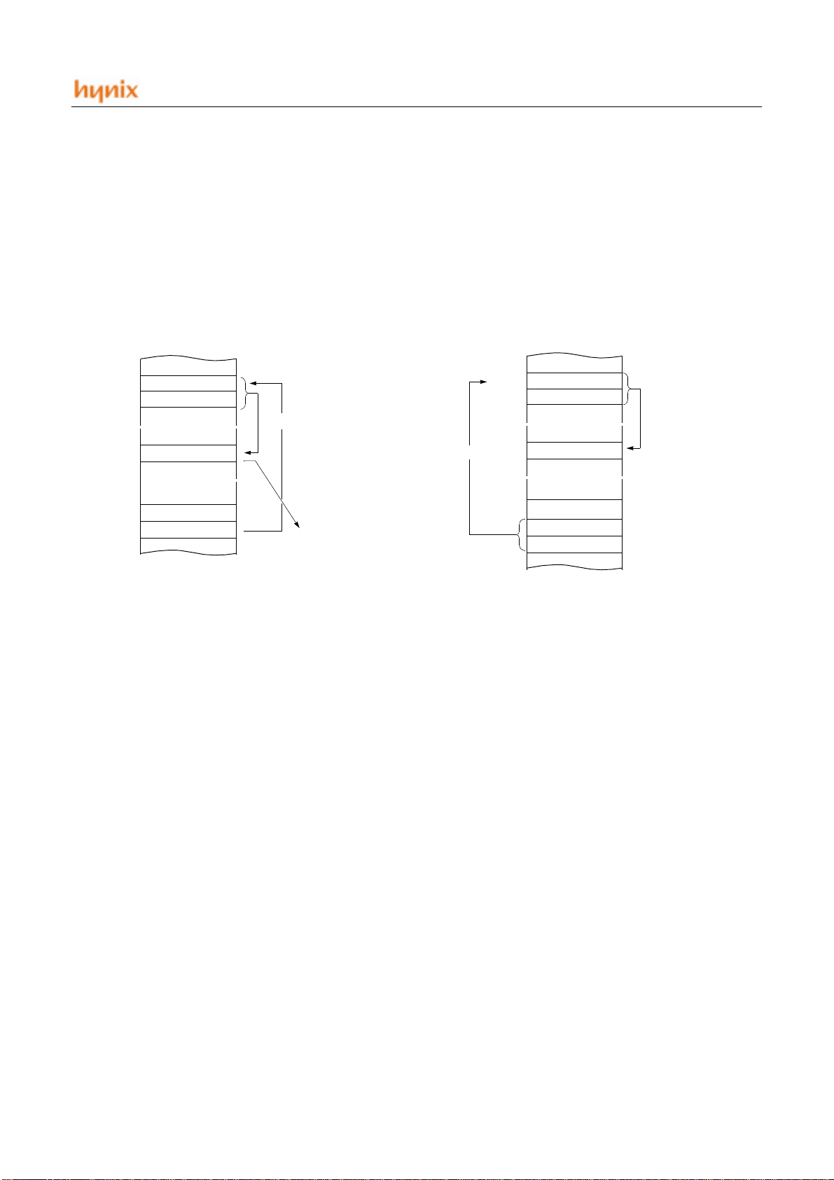
Y indexed indirect
→
→
→ →
[dp]+Y
Processes momory data as Data, assigned by the data
[dp+1][dp] of 16-bit p air memory paired by Operan d in Direct pageplus Y-register data.
ADC, AND, CMP, EOR, LDA, OR, SBC, STA
Example; G=0, Y=10
1725 ADC [25H]+Y
25
H
26
H
~
~
0E015
H
~
~
0FA00
H
05
E0
data
17
25
H
0E005H + Y(10) = 0E015
➋
~
~
H
➊
~
~
A + data + C → A
➌
Absolute indirect
→
→
→ →
[!abs]
The program jumps to address specified by 16-bit absolute
address.
JMP
Example; G=0
1F25E0 JMP [!0C025H]
JUNE 2001 Ver 1.00 29
Page 33
HMS81004E/08E/16E/24E/32E
9. I/O PORTS
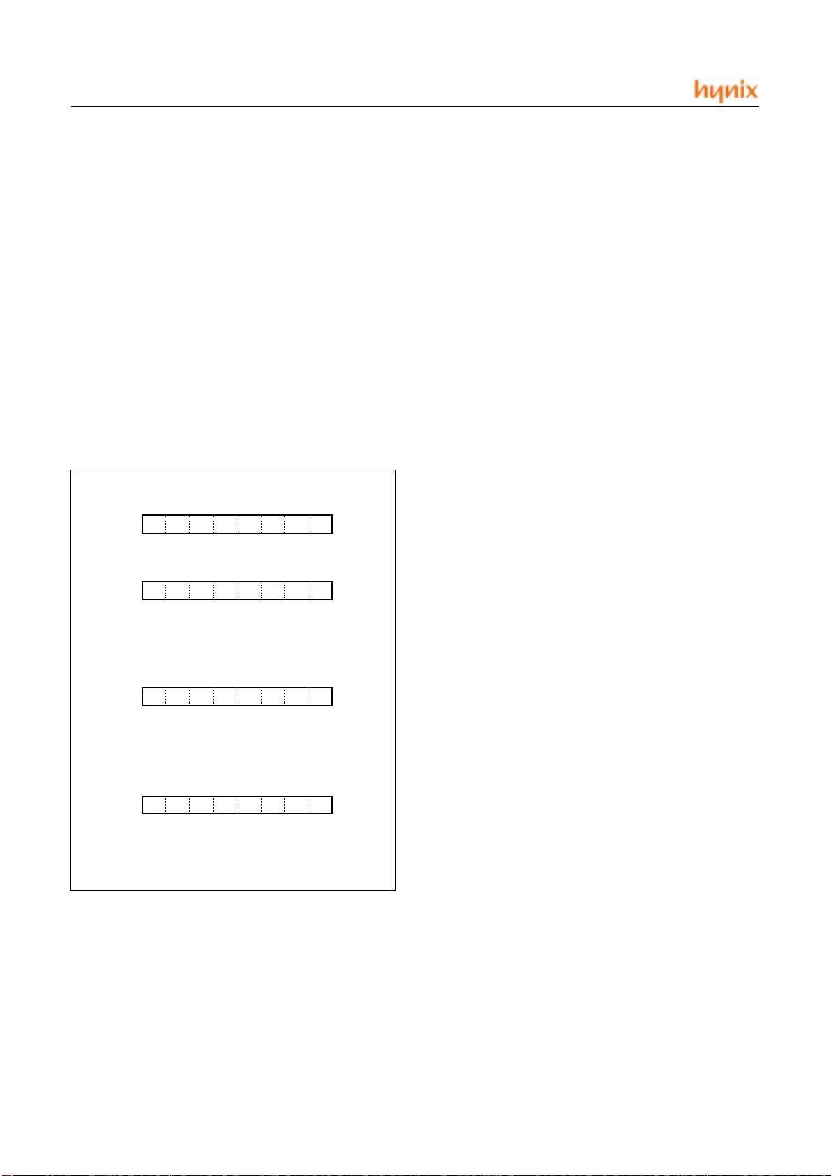
The HMS81004E/08E/16E/24E/32E has 24 I/O ports
which are PORT0(8 I/O), PORT1 (8 I/O), PORT2 (8 I/O).
Pull-up resistor of each port can be selectable by program.
Each port contains data d irect ion re gister which con trols I/
O and data register which stores port data.
9.1 R0 Ports
R0 is an 8-bit CMOS bidirectional I/O port (address
0C0
). Each I/O pin can indepe ndently used as an in put or
H
an output through the R0DD register (address 0C1
R0 has internal pull-ups that is independently connected or
disconnected by R0PC. The control registers for R0 are
shown below.
R0 Data Register (R/W)
R0
R0 Direction Register (W)
R0DD
R0 Pull-up Control Register (W)
R0PC
R07 R06 R05 R04 R03
ADDRESS : 0C0
RESET VALUE : Undefined
R02 R01
ADDRESS : 0C1
RESET VALUE : 00
ADDRESS :0F8
RESET VALUE : 00
R00
Port Direction
0: Input
1: Output
Pull-up select
1: Without pull-up
0: With pull-up
).
H
H
H
H
H
H
(1) R0 I/O Data Direction Register (R0DD)
R0 I/O Data Direction Register (R0DD) is 8-bit register,
and can assign input state or output state to each bit. If
R0DD is “1”, port R0 is in the output state, and if “0”, it is
in the input state. R0DD is write-only register. Since
R0DD is initialized as “00h” in reset state, the whole port
R0 becomes input state.
(2) R0 Data Register (R0)
R0 data register (R0) is 8-bit register to store data of port
R0. When set as the output state by R0DD, and data is written in R0, data is outputted into R0 pin. When set as the input state, input state of pin is read. The initial value of R0
is unknown in reset state.
(3) R0 Open drain Assign Register (R0ODC)
R0 Open Drain Assign Register (R0ODC) is 8bit register,
and can assign R0 port as open drain output port each bit,
if corresponding port is selected as output. If R0ODC is
selected as “1”, port R0 is open drain output, and if selected as, “0” it is push-pull output. R0ODC is write-only register and initialized as “00h” in reset state.
(4) R0 Pull-up Control Register (R0PC)
R0 Pull-up Control Register (R0PC) is 8-bit register and
can control pull-up on or off each bit, if corresponding port
is selected as input. If R0PC is selected as “1”, pull-up ia
disabled and if selected as “0”, it is enabled. R0PC is writeonly register and initiali zed as “00h” in reset state. The
pull-up is automatically disabl ed, if corresponding port is
selected as output.
R0 Open drain Assign Register (W)
R0ODC
ADDRESS :0E4
RESET VALUE : 00
H
H
Open drain select
0: Push-pull
1: Open drain
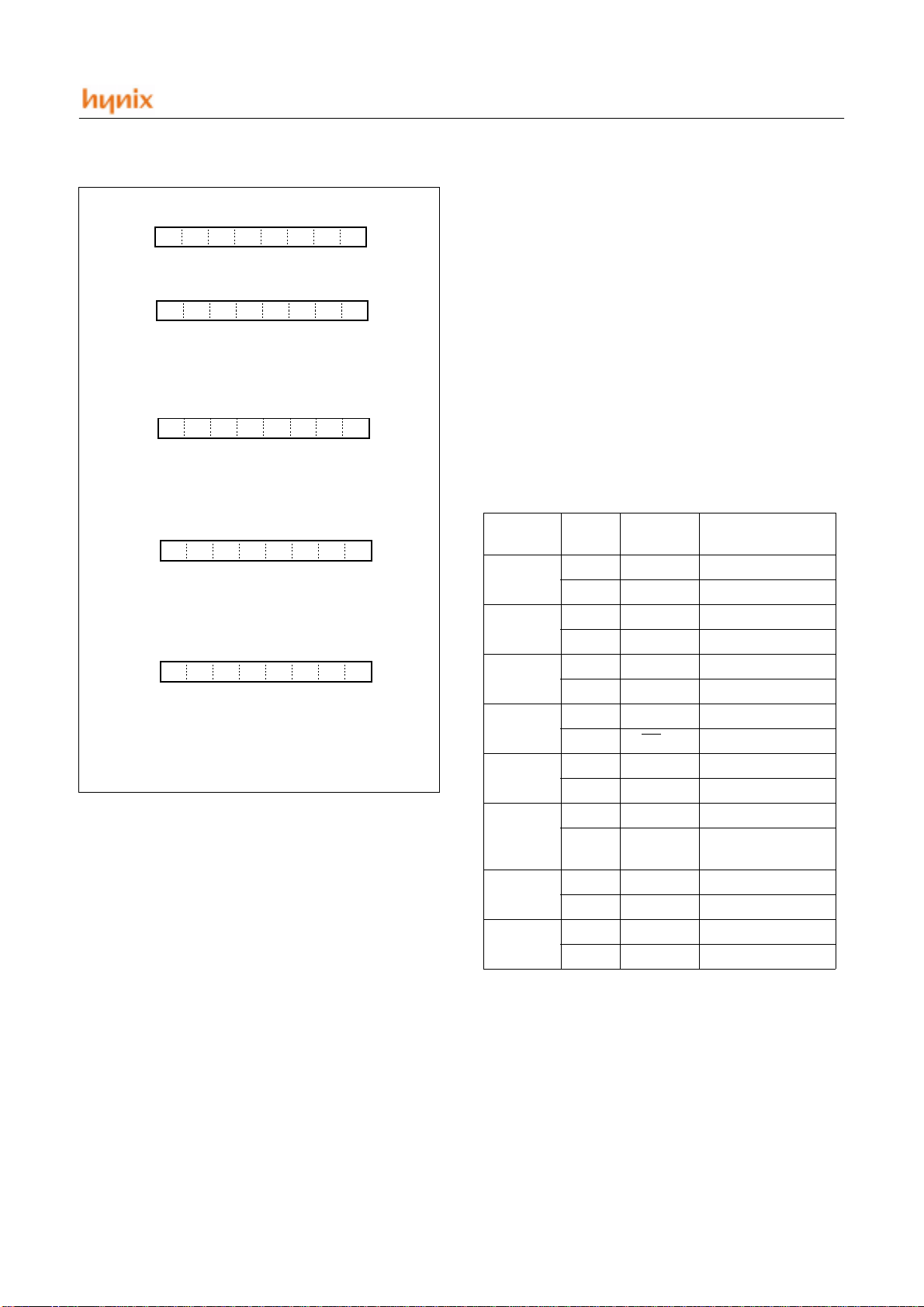
9.2 R1 Ports
R1 is an 8-bi t CMOS bidirectional I/ O port (address
0C2
). Each I/O pin can independently used as an input or
H
an output through the R1DD register (address 0C3
).
H
R1 has internal pull -ups that i s independ ently conne cted or
disconnected by register R1PC. The control registers for
R1 are shown below.
30 JUNE 2001 Ver 1.00
Page 34
R1 Data Register (R/W)
R1
R1 Direction Register (W)
R1DD
R1 Pull-up Control Register (W)
R1PC
R17 R16 R15 R14 R13 R12 R11 R10
ADDRESS : 0C2
RESET VALUE : Undefined
ADDRESS : 0C3
RESET VALUE : 00
ADDRESS : 0F9
RESET VALUE : 00
H
H
H
Port Direction
0: Input
1: Output
H
H
Pull-up select
1: Without pull-up
0: With pull-up
HMS81004E/08E/16E/24E/32E
and can assign R1 port as open drain output port each bit,
if corresponding port is selected as output. If R1ODC is
selected as “1”, port R1 is open drain output, and if selected as “0”, it is push-pull output. R1ODC is write-only register and initialized as “00h” in reset state.
(4) R1 Port Mode Register (PMR1)
R1 Port Mode Register (PMR1) is 8-bit register, and can
assign the selection mode for each bit. When set as “0”,
corresponding bit of PMR1 acts as port R1 selection mode,
and when set as “1”, it becomes function selection mode.
PMR1 is write-only register and initialized as “00h” in reset state. Therefore, becomes P ort selection mode. Port
R1 can be I/O port by manipulating each R1DD bit, if corresponding PMR1 bit is selected as “0”.
R1 Open drain Assign Register (W)
P1ODC
R1 Port Mode Register (W)
PMR1
ADDRESS : 0DE
RESET VALUE : 00
ADDRESS : 0C9
RESET VALUE : 00
H
H
Open drain select
0: Push-pull
1: Open drain
H
H
Mode select
0: Port R1 selection
1: Function selection
(1) R1 I/O Data Direction Register (R1DD)
R1 I/O Data Direction Register (R1DD) is 8-bit register,
and can assign input state or output state to eac h bit. If
R1DD is “1”, port R1 is in the output state, and if “0”, it is
in the input state. R1DD is write-only register. Since
R1DD is initialized as “00h” in reset state, the whole port
R1 becomes input state.
Pin Name PMR1
T0S
0 R17 (I/O) 1 T0 (O) Timer0
0 R16 (I/O) -
T1S
1 T1 (O) Timer1
0 R15 (I/O) -
T2S
ECS
1 T2 (O) Timer2
0 R14 (I/O) 1EC
0 R12 (I/O)
INT2S
1 INT2 (I)
0 R11 (I/O)
INT1S
1 INT1 (I)
Selection
Mode
(I) Timer0 Event
Timer0 Input Cap-
Remarks
ture
(2) R1 Data Register (R1)
Table 9-1 Selection mode of PMR1
R1 data register (R1) is 8-bit register to store data of port
R1. When set as the output state by R1DD, and data is
written in R1, data is outputted into R1 pin. When set as
the input state, input state of pin is read. The initial va lue
of R1 is unknown in reset state.
(5) R1 Pull-up Control Register (R1PC)
R1 Pull-up Control Register (R1PC) is 8-bit register and
can control pull-up on or off each bit, if corresponding port
is selected as input. If R1PC is selected as “1”, pull-up ia
(3) R1 Open drain Assign Register (R1ODC)
R1 Open Drain Assign Register (R1ODC) is 8bit register,
disabled and if selected as “0”, it is enabled. R1PC is writeonly register and initiali zed as “00h” in reset state. The
JUNE 2001 Ver 1.00 31
Page 35

HMS81004E/08E/16E/24E/32E
pull-up is automatically disabled, if corresponding port is
selected as output.
9.3 R2 Port
R2 is an 8-bit CMOS bidirectional I/O port (address
0C4
). Each I/O pin can indepe ndently used as an in put or
H
an output through the R2DD register (address 0C5
R2 has internal pujll-ups that is independently connected
or disconnected by R2PC (ad dress 0FA
). The control reg-
H
isters for R2 are shown as below.
R2 Data Register (R/W)
--
R2
R2 Direction Register (W)
R2DD
R2 Pull-up Control Register (W)
R2PC
R2 Open drain Assign Register (W)
R2ODC
-
ADDRESS : 0C4
RESET VALUE : Undefined
R23 R22 R21 R20
R24
ADDRESS : 0C5
RESET VALUE : 00
ADDRESS :0FA
RESET VALUE : 00
ADDRESS :0DF
RESET VALUE : 00
Port Direction
0: Input
1: Output
Pull-up select
1: Without pull-up
0: With pull-up
Open drain select
0: Push-pull
1: Open drain
).
H
H
H
H
H
H
H
H
(1) R2 I/O Data Direction Register (R2DD)
R2 I/O Data Direction Register (R2DD) is 8-bit register,
and can assign input state or output state to each bit. If
R2DD is “1”, port R2 is in the output state, and if “0”, it is
in the input state. R2DD is write-only register. Since
R2DD is initialized as “00h” in reset state, the whole port
R2 becomes input state.
(2) R2 Data Register (R2)
R2 data register (R2) is 8-bit register to store data of port
R2. When set as the output state by R2DD, and data is written in R2, data is outputted into R2 pin. When set as the input state, input state of pin is read. The initial value of R2
is unknown in reset state.
(3) R2 Open drain Assign Register (R2ODC)
R2 Open Drain Assign Register (R2ODC) is 8bit register,
and can assign R2 port as open drain output port each bit,
if corresponding port is selected as output. If R2ODC is
selected as “1”, port R2 is open drain output, and if selected as “0”, it is push-pull output. R2ODC is write-only register and initialized as “00h” in reset state.
(4) R2 Pull-up Control Register (R2PC)
R2 Pull-up Control Register (R2PC) is 8-bit register and
can control pull-up on or off each bit, if corresponding port
is selected as input. If R2PC is selected as “1”, pull-up ia
disabled and if selected as ”0”, it is enabled. R2PC is writeonly register and initiali zed as “00h” in reset state. The
pull-up is automatically disabl ed, if corresponding port is
selected as output.
32 JUNE 2001 Ver 1.00
Page 36
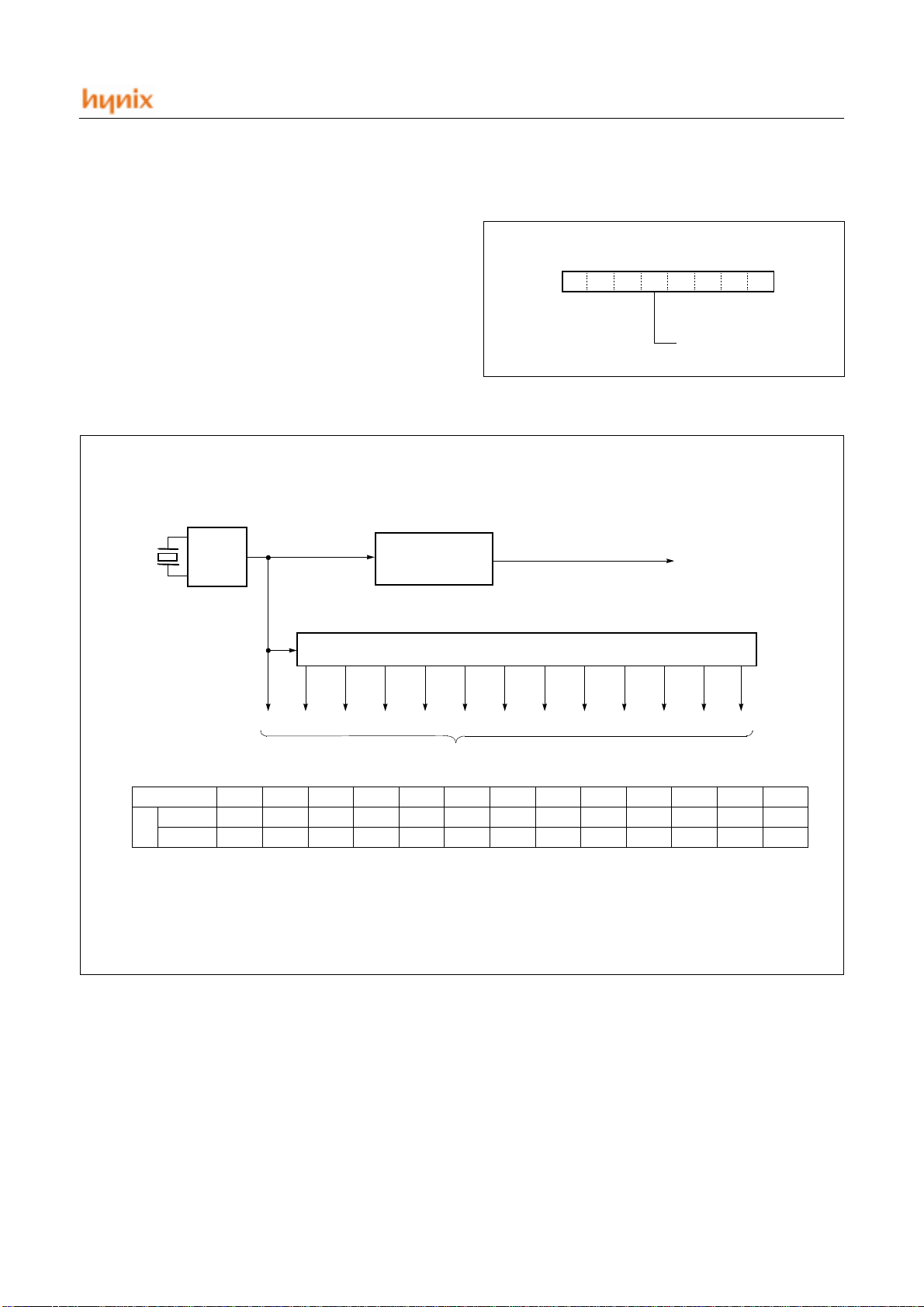
10. CLOCK GENERATOR
Clock Control Register (W)
CKCTLR
ADDRESS : 0C7
H
INITIAL VALUE : --110111b
0
123
4567
ENPCK 0: Stopped
1: Provided
HMS81004E/08E/16E/24E/32E
Clock generating circuit con sists of Clo ck Pulse Generato r
(C.P.G), Prescaler, Basic Interval Timer (B.I.T) and Watch
Dog Timer. The clock applied to the Xin pin divided by
two is used as the internal system clock.
Prescaler consist of 12-bit binary counter. The clock supplied from oscillation circuit is input to prescaler(fex)
The divided output from each bit of prescaler is provided
to periphera hardwarel
Clock to pe ripheral hardware can be stopped by bit4 (ENPCK) of CKCTLR Register. ENPCK is set to “1” in reset
OSC
CIRCUIT
fex
PS0 PS1 PS2 PS3 PS4 PS5 PS6 PS7 PS8 PS9 PS10
CLOCK PULSE
GENERATOR
state.
PRESCALER
Internal system clock (CPU clock)
PS11
PS12
fEX(MHz)
Frequency
4
period
1
2
÷
÷
PS0 PS3PS2 PS4PS1 PS10PS9PS5 PS6 PS7
4M 1M 500K 250K2M 125K 62.5K
250n 500n 1u 2u 4u 8u 16u 32u 64u 256u128u
4
÷
÷8÷
16
32÷64
÷
Peripheral clock
128÷256÷512÷1024
÷
PS8
Figure 10-1 Block diagram of Clock Generator
2048÷4096
÷
3.906K7.183K15.63K31.25K
PS11 PS12
1.953K
0.976K
1024u
512u
JUNE 2001 Ver 1.00 33
Page 37
HMS81004E/08E/16E/24E/32E
X
OUT
X
IN
10.1 Oscillation Circuit
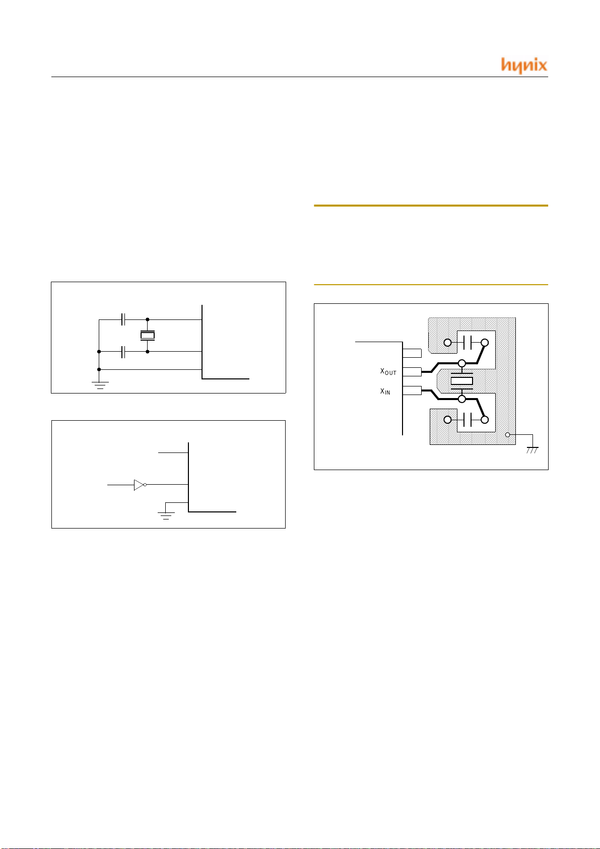
Oscillation circuit is designed to be used either with a ceramic resonator or crystal oscillator. Figure 10-2 shows
circuit diagrams using a crystal (or ceramic) oscillator. As
shown in the diagram, oscillation circuits can be constructed by connecting a oscillator between Xout and Xin. Colck
from oscillation circuit makesCPU clock via clock pulse
generator, and then enters prescaler to make per ipheral
hardware clock. Alternately, the oscillator may b e driven
from an esternal source as Figure 10-3 . In the ST OP
mode,oscillation stop, Xout state goes to “HIGH” , Xin
state goes to “LOW” , and built-in feed back resistor is disabled.
Oscillation circuit is design ed to be u sed either with a ceramic resonator or crystal oscillator. Since each crystal and
ceramic resonator have their own characteristics, the user
should consult the crystal manufacturer for appropriate
values of external components. In addition, see Figure 104 for the layout of the crystal.
Note: Minimize the wiring length. Do not allo w the wiring to
intersect with other signal co ndu ctors. Do not allo w the wi ring to come near changi ng high cu rrent. Set t he potentia l of
the grounding position of the oscillator capacitor to that of
VSS. Do not ground it to any groun d pattern w here high current is present. Do not fetch signals from the oscillator.
Cout
Cin
Xout
Xin
Vss
Figure 10-2 External Crystal(Ceramic) oscillator circuit
Xout
Xin
Vss
External
Clock
Source
OPEN
Figure 10-3 External clock input circuit
Figure 10-4 Recommend Layout of Oscillator PCB
circuit
34 JUNE 2001 Ver 1.00
Page 38
HMS81004E/08E/16E/24E/32E
Frequency Resonator Maker Part Name Load Capacitor Operating Voltage
CQ ZTT2.00 Cin=Cout=open 2.0~3.6
CQ ZTA2.00 Cin=Cout=30pF 2.0~3.6
2.00MHz
4.00MHz
MURATA CSTLS2M00G56-B0 Cin=Cout=open 2.0~3.6
MURATA CSTCC2.00MG0H6 Cin=Cout=open 2.0~3.6
MURATA CSTCC2M00G56-R0 Cin=Cout=open 2.0~3.6
CQ ZTT4.00 Cin=Cout=open 2.0~3.6
CQ ZTA4.00 Cin=Cout=30pF 2.0~3.6
MURATA CSTS0400MG06 Cin=Cout=open 2.0~3.6
MURATA CSTLS4M00G56-B0 Cin=Cout=open 2.0~3.6
MURATA CSTCR4M00G55-R0 Cin=Cout=open 2.0~3.6
TDK FCR4.0MC5 Cin=Cout=open 2.0~3.6
TDK FCR4.0MSC5 Cin=Cout=open 2.0~3.6
CORETECK CRT4.00MS Cin=Cout=open 2.0~3.6
CORETECK CRM4.00MS Cin=Cout=30pF 2.0~3.6
Table 10-1 Recommendalbe resonator
JUNE 2001 Ver 1.00 35
Page 39
HMS81004E/08E/16E/24E/32E
11. BASIC INTERVAL TIMER
The HMS81004E/08E/16E/24E/32E has one 8-bit Basic
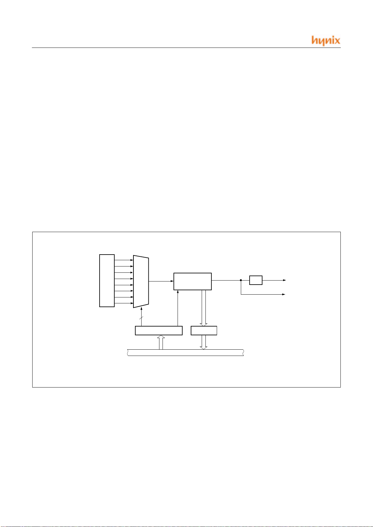
Interval Timer that is free-run and can n ot stop. Blo ck d iagram is shown in Figure 11-1 .
The Basic Interval Timer generates the time base for
Standby release time, watchdog ti m er coun ti n g, and et c. It
also provides a Basic interval timer interrupt (IFBIT). As
the count overflow from FF
to 00H, this overflow causes
H
the interrupt to be generated.
-8bit binary up-counter
-Use the bit output of prescaler as input to secure the oscillation stabilization time after power-on
-Secures the oscillation stabilization time in standby mode
(stop mode) release
-Contents of B.I.T can be read
-Provides the clock for watch dog timer
8
÷
16
÷
32
÷
64
÷
128
÷
256
÷
Prescaler
512
÷
1024
÷
MUX
source
clock
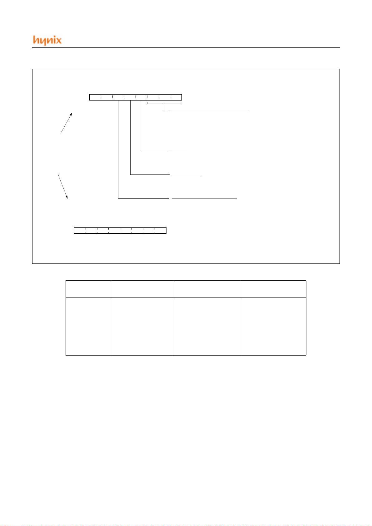
The Basic Interval Timer is controlled by th e clock control
register (CKCTLR) shown in Figure 11-2 . If bit3(BTCL)
of CKCTLR is set to “1”, B.I.T is cleared, and then, after
one machine cycle, BTCL be comes “0”, and B.I.T starts
counting. BTCL is set to ``0`` in reset state.
The input clock of B.I.T can be selected from th e prescaler
within a range of 2us to 256us by clock i nput selecti on bits
(BTS2~BTS0). (at fex = 4MHz). In reset state, or power
on reset, BTS2=“1”, BTS1= “1”, BTS0= “1” to secure the
longest oscillation stabilization time. B.I.T can generate
the wide range of basic interval time interrupt reques t (IF BIT) by selecting prescaler output.
By reading of the Basic Interval Timer Register (BITR),
we can read counter value of B.I.T. Because B.I.T can be
cleared or read, the spending time up to maximum 65.5ms
can be available. B.I.T is read-only register. If B.I.T register is written, then CKCTLR register with same address
is written.
Basic Interval Timer
8-bit up-counter
clear
overflow
IFBIT
Basic Interval Timer Interrupt
To Watchdog timer (WDTR)
Select Input clock
[0C7
clock control register
3
BTS[2:0]
CKCTLR
]
H
BTCL
BITR
Read
Internal bus line
Figure 11-1 Block diagram of Basic Interval Timer
36 JUNE 2001 Ver 1.00
Page 40
CKCTLR
76543210
Caution:
Both register are in same address,
when write, to be a CKCTLR,
when read, to be a BITR.
--
W
WDTON
WW WWW
BTCL
ENPCK
BTCL
HMS81004E/08E/16E/24E/32E
BTS1
BTS0BTS2
Basic Interval Timer source clock select
000: f
001: f
010: f
011: f
100: f
101: f
110: f
111: f
Clear bit
0: Normal operation, free-run
1: Clear 8-bit counter (BITR) to “0” and count up again.
Periphral clock
0:stopped
1:provided
Watch Dog Timer function control
0:6bit timer
1:Watch Do g Timer
ADDRESS: 0C7
INITAIL VALUE: --110111
÷ 8
XIN
÷ 16
XIN
÷ 32
XIN
÷ 64
XIN
÷ 128
XIN
÷ 256
XIN
÷ 512
XIN
÷ 1024
XIN
This bit becomes to “0” automatically after one machine cycle.
H
B
BITR
RR RRR RR
76543210
R
BTCL
8-BIT FREE-RUN BINARY COUNTER
Figure 11-2 CKCTLR AND BITR
BTS[2:0] CPU Source clock
000
001
010
011
100
101
110
111
÷
÷
16
÷
32
÷
64
÷
128
÷
256
÷
512
÷
1024
8
ADDRESS: 0C7
INITIAL VALUE: Undefined
H
B.I.T. Input
clock@4Mhz(us)
16
32
64
128
256
Standby release
2
4
8
time(ms)
0.512
1.024
2.048
4.096
8.192
16.384
32.768
65.536
JUNE 2001 Ver 1.00 37
Page 41
HMS81004E/08E/16E/24E/32E
12. WATCH DOG TIMER
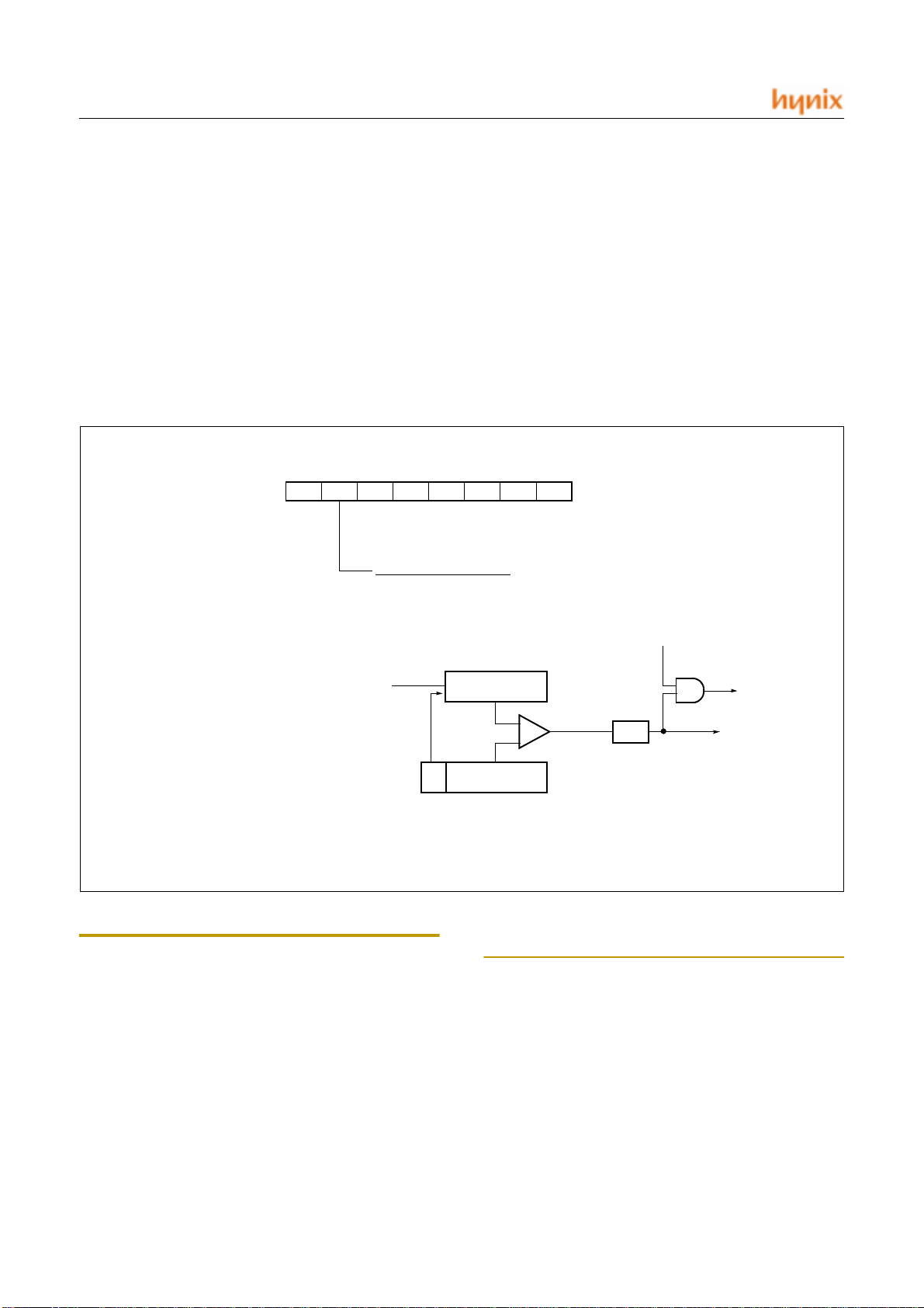
Watch Dog Timer (WDT) consists of 6- bit bi nary coun ter,
6-bit comparator, and Watch Dog Timer Register
(WDTR).Watch Dog Timer can be used 6-bit genera l Timer or specific Watch dog timer by setting bit5 (WDTON)
of Clock Control Register (CKCTLR).By assigning
bit6(WDTCL) of WDTR, 6-bit counter can be cleared.
WDT Interrupt (IFWDT) interval is determined by the interrupt IFBIT interval of Basic Interval Timer and the value of WDT Register.
-Interval of IFWDT = (IFBIT interval) * (WDTR value)
76543210
WDTR
WDTCL
-
WDTR5 WDTR4 WDTR3
Watch Dog Timer Operation
0:Free-run
1:Automatically cleared, after one machine cycle
BTCL
As IFBIT (Basic Interval Timer Interrupt Request) is used
for input clock of WDT, Input clock cycle is possible from
512 us to 65,536 us by BTS. (at fex = 4MHz)
*At Hardware reset time,WDT starts automatically.
Therefore the user must select the CKCTLR and WD TR
before WDT overflow.
-Reset WDTR value = 0F
,=15
h
-Interval of WDT = 65,536 * 15 = 983040 us
(about 1second )
WDTR2
WDTR1 WDTR0
ADDRESS: 0C8
INITIAL VALUE: -0001111
H
b
WDTON
IFBIT
Clear
Figure 12-1 Block diagram of Watch Dog Timer
Note: When WDTR Register value is 63 (3Fh)
(Caution) : Do not use “0” f or WDTR Register value.
6
[0C8H]
WDT (6-bit)
Comparator
WDTR (6-bit)
IFWDT
WDT
Device come into the reset state by WDT
To Reset circuit
WDT
INTERRUPT
38 JUNE 2001 Ver 1.00
Page 42
13. Timer0, Timer1, Timer2
HMS81004E/08E/16E/24E/32E
(1) Timer Operation Mode
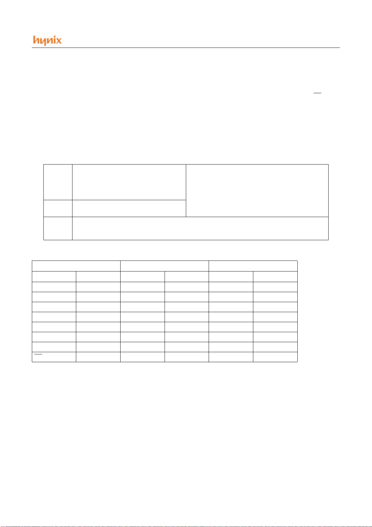
Timer consists of 16bit binary counter Timer0 (T0), 8bit
binary Timer1 (T1), Timer2 (T2), Timer Data Register,
Timer Mode Register (TM01, TM0, TM1 , TM2) an d con trol circuit. Timer Data Register Consists of Timer0 HighMSB Data Register (T0HMD), Timer0 High-LS B Data
Register (T0HLD), Timer0 Low-MSB Data Register
(T0LMD), Timer0 Low-LSB Data Register (T0LLD),
Timer1 High Data Register (T1HD), Timer1 Low Data
- 16-bit Interval Timer
- 16-bit Event Counter
Timer0
Timer1
Timer2
16bit Timer (T0) 8bit Timer (T1) 8bit Timer (T2)
- 16-bit Input Capture
- 16-bit rectangular-wave output
- 8-bit Interval Timer
- 8-bit rectangular-wave output
- 8-bit Interval Timer
- 8-bit rectangular-wave output
- Modulo-N Mode
Table 13-1 Timer Operation
Register (T1LD), Timer2 Data Register (T2DR). Any of
the PS0 ~ PS5, PS11 and external event input EC
can be
selected as clock source for T0. Any of the PS0 ~ PS3, PS7
~ PS10 can be selected as clock T1. Any of the PS5 ~ PS12
can be selected as clock source for T2.
* Relevant Port Mode Re gister (PMR1 : 00C9h) v alue
should be assigned for event counter.
- Single/Modulo-N Mode
- Timer Output Initial Value Setting
- Timer0~Timer1 combination Logic Output
- One Interrupt Generating Every 2nd
Counter Overflow
Resolution MAX. Count Resolution MAX. Count Resolution MAX. Count
PS0 (0.25us) 16,384us PS0 (0.25us) 64us PS5 (8us) 2,048us
PS1 (0.5us) 32,768us PS1 (0.5us) 128us PS6 (16us) 4,096us
PS2 (1us) 65,536us PS2 (1us) 256us PS7 (32us) 8,192us
PS3 (2us) 131,072us PS3 (2us) 512us PS8 (64us) 16,384us
PS4 (4us) 262,144us PS7 (32us) 8,192us PS9 (128us) 32,768us
PS5 (8us) 524,288us PS8 (64us) 16,384us PS10 (256us) 65,536us
PS11 (512us) 33,554,432us PS9 (128us) 32,768us PS11 (512us) 131,072us
EC
- PS10 (256us) 65,536us PS12 (1024us) 262,144us
Table 13-2 Function of Timer & Counter
JUNE 2001 Ver 1.00 39
Page 43
HMS81004E/08E/16E/24E/32E
from
/R14
EC
from
INT2/R12
(Capture Signal)
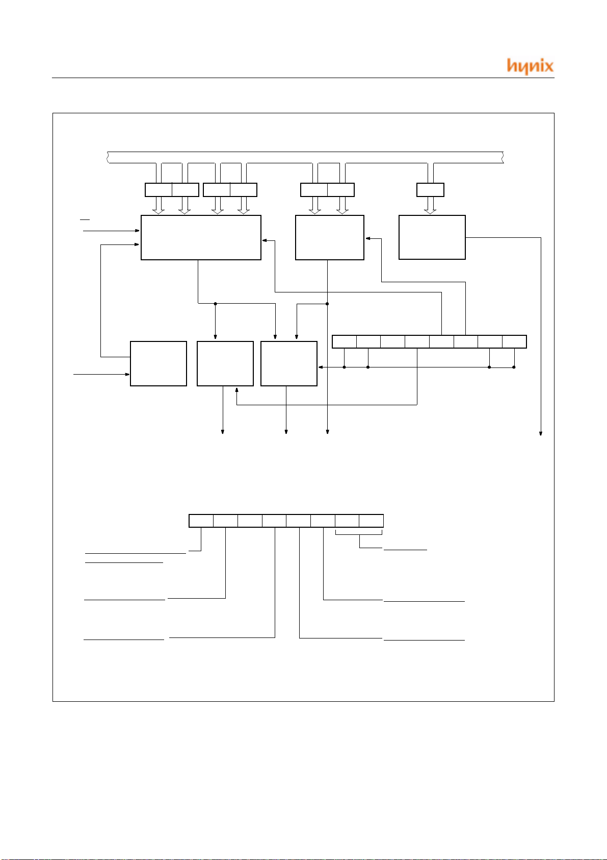
T0HMD T0LMD T0LMD T0LLD
Timer0 (16bit)
Edge
Selection
Polarity
Selection
T0OUT
(R17)
Timer1(8bit)
Tout
Logic
TOUT
(REMOUT)
T1HD T1LD T2DR
Timer2(8bit)
70
TOUTS TOUTB
T1OUT
(R16)
T0OUTP
TM01
T0 IN IT T1 INIT
BTCL-TOUT1TOUT0
T2OUT
(R15)
Timer 01 mode register
TM01
REMOUT Port Output Selection
(TOUT Logic or TOUTB)
0: Bit(TOUTB) Output Through REMOUT
1: TOUT Logic Output Through REMOUT
REMOUT Port Bit Control
0: REMOUT Output Low
1: REMOUT Output High
T0OUT Polarity Selection
0: T0OUT Polarity Equal to TOUT Logic input signal
1: T0OUT Polarity Reverse to TOUT Logic input signal
R/WR/W
76543210
TOUTS TOUTB
Figure 13-1 Block Diagram of Timer/Counter
R/W R/W R/W R/W R/W
T0 IN IT T 1INIT
T0OUT P
-
BTCL
TOUT1 TO UT0
ADDRESS: 0DA
INITIAL VALUE: 00
TOUT LOGIC
00: AND of T0 OUTPUT and T1 OUTPUT
01: NAND of T0 OUTPUT and T1 OUTPUT
10: OR of T0 OUTPUT and T1 OUTPUT
11: NOR of T0 OUTPUT and T1 OUTPUT
Timer1 output initial value
0: Timer1 output low
1: Timer1 output high
Timer0 output initial value
0: Timer0 output low
1: Timer0 output high
H
H
40 JUNE 2001 Ver 1.00
Page 44
HMS81004E/08E/16E/24E/32E
IEDS[5:4]
INT2/R12 PIN
EC PIN
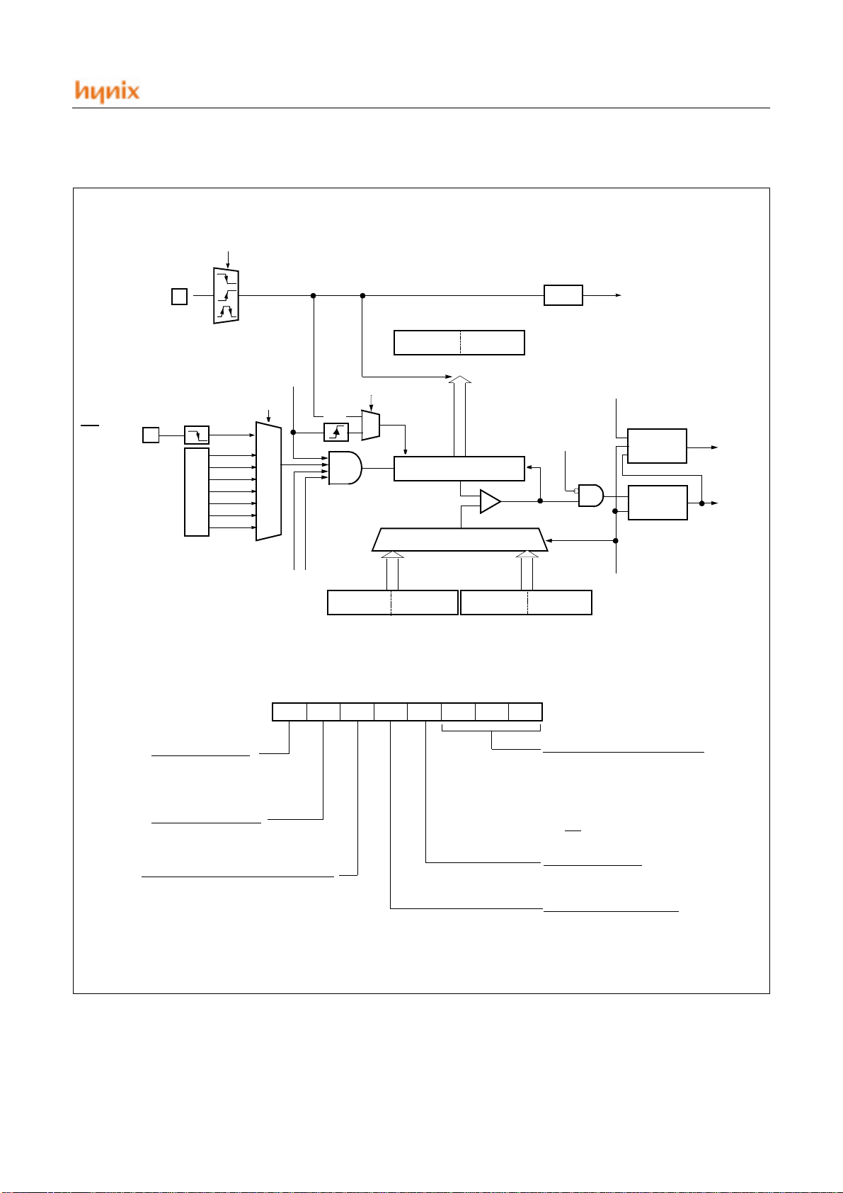
Timer 0 mode register
TM0
Edge Detector
PS11
PS5
PS4
PS3
PS2
PS1
Prescaler
PS0
01
10
11
T0 SL [2 :0]
111
110
101
100
011
010
001
000
MUX
16 BITSMSB LSB
T0ST
T0MOD T0CN
delay
CAP0
1
0
T0HC T0LC
capture
clear
T0 COUNTER (16-bit)
1
MUX(16-bit)
[0D5
clear
Comparator
0
T0HMD T0HLD T0LMD T0LLD
[0D5
][0D6H]
[0D3H][0D4H]
R/W R/W R/W R/W R/W R/W
R/WR/W
H
76543210
CAP0 T0ST
T0CN T0IFS
T0MOD
BTCL
T0SL2 T0SL1 T0SL0
IFINT2
][0D6H]
H
T0IFS
CAP0
T0INIT
ADDRESS: 0D0
INITIAL VALUE: 00
INT2
INTERRUPT
Interrupt
GEN.
OUTPUT
GEN.
H
H
IFT0
T0OUT
Timer0 Interrupt select
0: Timer/Co unter
1: Input capture (PS1:not support ing
input cature)
Timer0 Start/Stop control
0: Timer0 Stop
1: Tiemr0 Start after clear
Timer0 input clock select (fex=4Mhz)
000: PS0 250ns
001: PS1 500ns
010: PS2 1us
011: PS3 2us
100: PS4 4us
101: PS5 8us
110: PS11 512us
111: EC
Timer0 Interrupt selec t
Timer0 Counter Continuation/Pause Control
0: Count Pause
1: Count Continuation
0: Interrupt Every Count Overflow
1: Interrupt Every 2nd Count Overflow
Timer0 Single/Moudol-N select
0: Modulo-N
1: Single Mode
Figure 13-2 Block Diagram of Timer0
JUNE 2001 Ver 1.00 41
Page 45
HMS81004E/08E/16E/24E/32E
T1ST
T1 SL [2 :0]
PS10
PS9
PS8
PS7
PS3
PS2
Prescaler
PS1
PS0
111
110
101
100
011
010
001
000
MUX
T1MOD T1CN
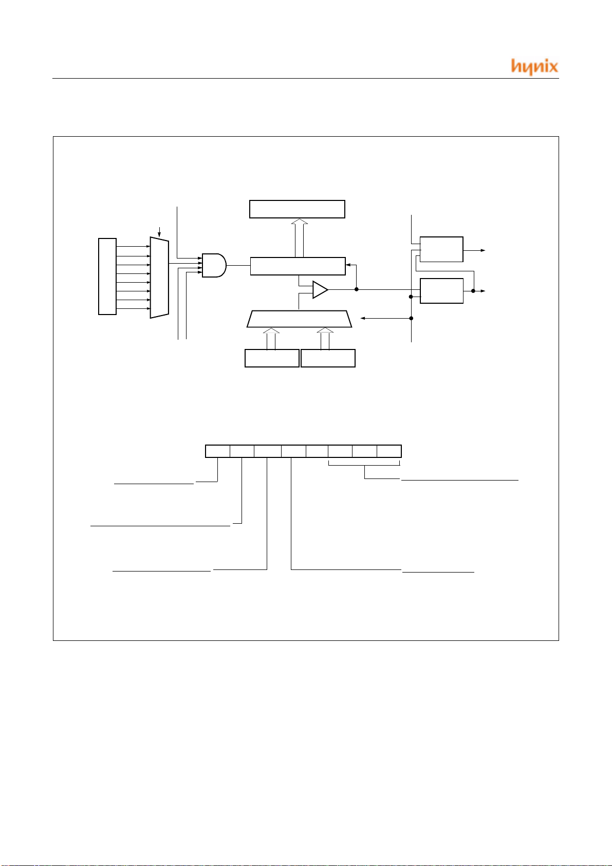
Timer 1 mode register
76543210
TM1
Timer1 Start/Stop control
0: Timer1 Stop
1: Tiemr1 Start after clear
Timer1 Counter Continuation/Pause Control
0: Count Pause
1: Count Continuation
T1ST
T1 COUNT REG.
[0D8H]
T1 COUNTER (8-bit)
Comparator
MUX(8-bit)
10
T1HD(8-bit) T1LD(8-bit)
[0D7H][0D8
R/W R/W R/W R/W R/W
R/WR/W
T1CN
T1MOD
T1IFS
H
-
BTCL
T1SL2 T1SL1 T 1SL0
T1IFS
clear
T1INIT
Interrupt
GEN.
OUTPUT
GEN.
IFT1
T1OUT
]
ADDRESS: 0D1
INITIAL VALUE: 00
H
H
Timer1 input clock select (fex=4Mhz)
000: PS0 250ns
001: PS1 500ns
010: PS2 1us
011: PS3 2us
100: PS7 32us
101: PS8 64us
110: PS9 128us
111: PS10 256us
Timer1 Single/Moudol-N select
0: Modulo-N
1: Single Mode
Timer1 Interrupt select
0: Interrupt Every Count Overflow
1: Interrupt Every 2nd Count Overflow
Figure 13-3 Block Diagram of Timer1
42 JUNE 2001 Ver 1.00
Page 46
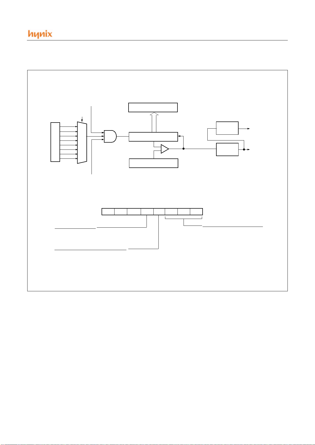
HMS81004E/08E/16E/24E/32E
T2ST
T2 SL [2 :0]
PS12
PS11
PS10
PS9
PS8
PS7
Prescaler
PS6
PS5
111
110
101
100
011
010
001
000
MUX
T2CN
Timer 2 mode register
76543210
TM2
Timer2 Start/Stop control
0: Timer2 Stop
1: Tiemr2 Start after clear
Timer2 Counter Continuation/Pause Control
0: Count Pause
1: Count Continuation
-
T2 COUNT REG.
[0D9H]
T2 COUNTER (8-bit)
Comparator
clear
Interrupt
GEN.
OUTPUT
GEN.
IFT2
T2OUT
T2DR
]
[0D9
H
R/W R/W R/W R/W R/W
-
-
T2ST
BTCL
T2CN
T2SL2 T2SL1 T2SL0
ADDRESS: 0D2
INITIAL VALUE: 00
H
H
Timer2 input clock select (fex=4Mhz)
000: PS5 8us
001: PS6 16us
010: PS7 32us
011: PS8 64us
100: PS9 128us
101: PS10 256us
110: PS11 512us
111: PS12 1,024us
Figure 13-4 Block Diagram of Timer2
JUNE 2001 Ver 1.00 43
Page 47
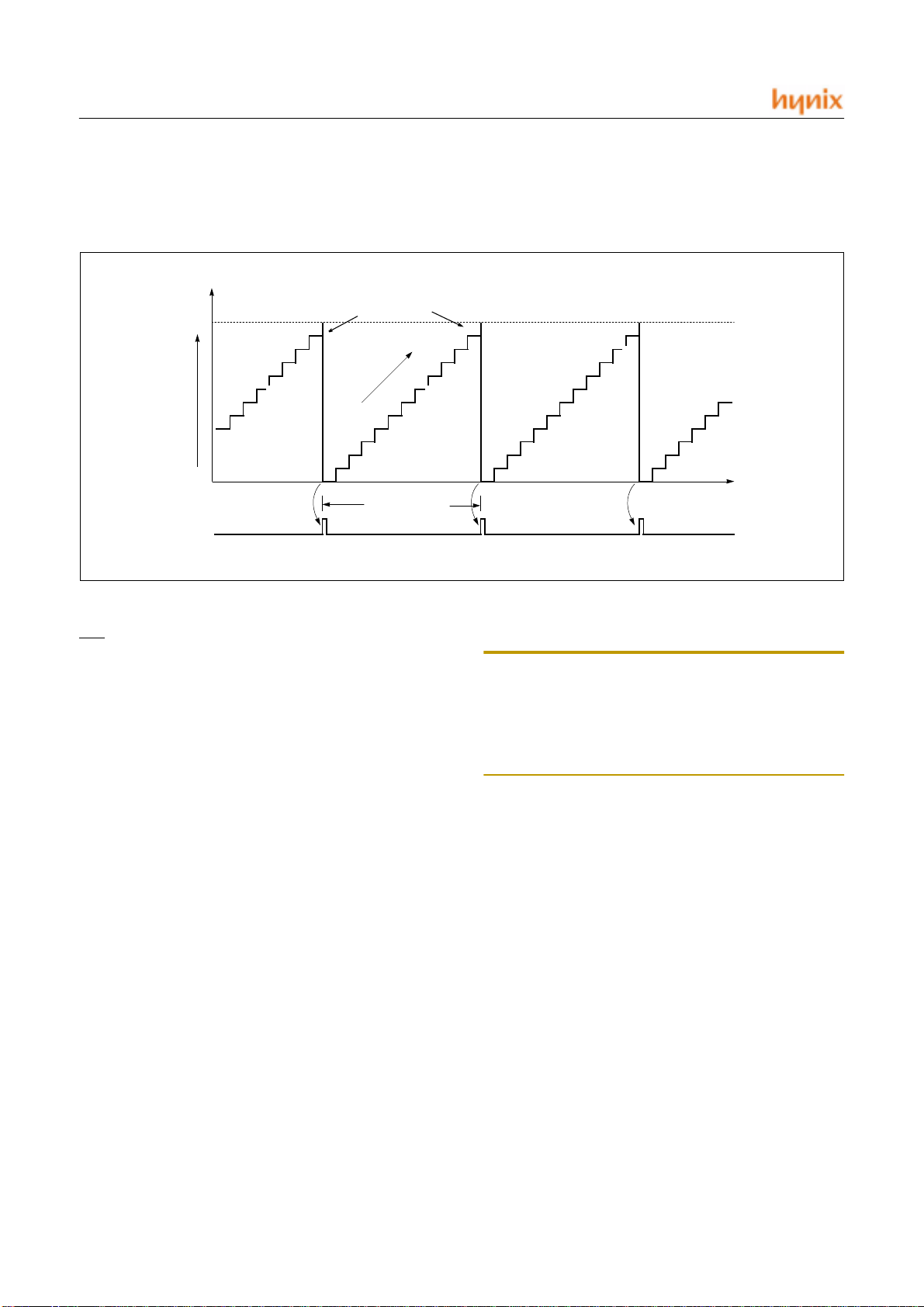
HMS81004E/08E/16E/24E/32E
2) Timer0, Timer1
TIMER0 and TIMER1 have an up-counter. When val ue of
the up-counter reaches the content of Timer Data Register
T0 Data
Register
Value
T0 Value
0
Timer 0 (IFT0)
Interrupt
~
~
0
Occur interrupt Occur interrupt Occur interrupt
MATCH
(TDR = T0)
up-count
3
2
1
~
~
6
5
4
Interrupt period
Figure 13-5 Operation of Timer0
For Timer0, the internal clock (PS) and the external clock
) can be selected as counter clock. But Timer 1 and
(EC
Timer2 use only internal clock. As internal clock. Timer0
can be used as internal-timer which period is determined
by Timer Data Re gister (TDR). Chosen as e xternal
clock, Timer0 executes as event-counter. The counter execution of Timer0 and Timer1 is controlled by T0CN,
T0ST, CAP0, T1CN, T1ST, of Timer Mode Regi ster TM0
and TM1. T0CN, T1CN are used to stop and start Timer0
and Timer1 without clearing the counter. T0ST, T1ST is
used to clear the counter. For cleari ng and starting the
counter, T0ST or T1ST should be temporarily set to “0 ”
and then set to “1”. T0CN, T1CN, T0ST and T1ST should
be set “1”, w hen Timer coun ting-up. Contr olling of
CAP0 enables Timer0 as input capture. By programming
of CAP0 to “1”, the period of signal from INT2 can be
measured and then, event counter value for INT2 can be
read. During counting-up, value of counter can be readTimer execution is stopped by the reset signal(RE-
(TDR), the up-counter is clear ed to “00h”, and interrupt
(IFT0, IFT1) is occured at the next clock.
~
~
TIME
SET=”L”)
Note: In the process of reading 16-bit Timer Data, first
read the upper 8-bit data. Then read the lower 8-bit data,
and read the upper 8-bit data again. If the earlier read upper 8-bit data are matched with the later read upper 8-bit
data, read 16-bit data are correct. If not, caution should be
taken in the selection of upper 8-bit data.
(Example)
1) Upper 8-bit Read 0A 0A
2) Lower 8-bit Read FF 01
3) Upper 8-bit Read 0B 0B
=====================
0AFF 0B01
44 JUNE 2001 Ver 1.00
Page 48
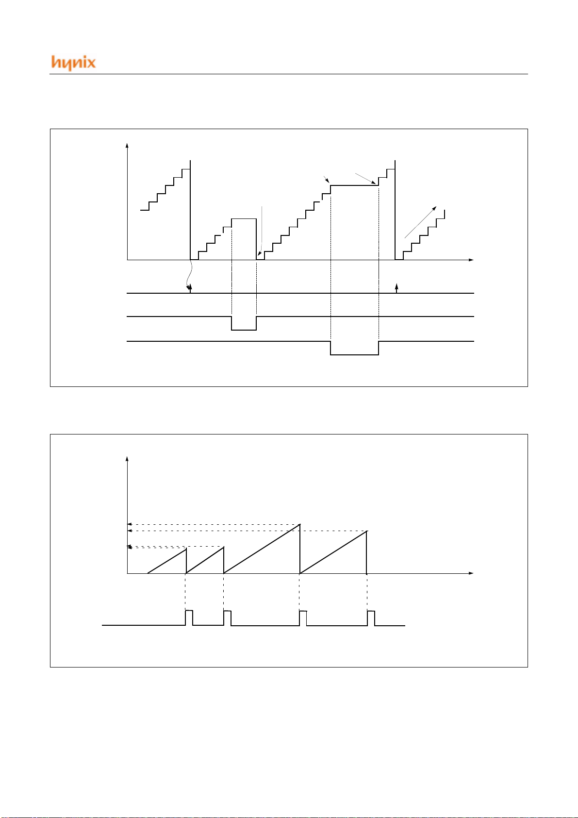
HMS81004E/08E/16E/24E/32E
TDR
Timer 0 (IFT0)
Interrupt
T0ST
Start & St op
T0CN
Control count
disable
clear & start
stop
~
~
Occur interrupt Occur interrupt
T0ST = 1
T0ST = 0
enable
~
~
up-count
T0CN = 1
T0CN = 0
Figure 13-6 Start/Stop Operation of Timer0
TIME
T2
T3
T1
T0
INT2
Figure 13-7 Input capture operation of Timer0
JUNE 2001 Ver 1.00 45
Page 49
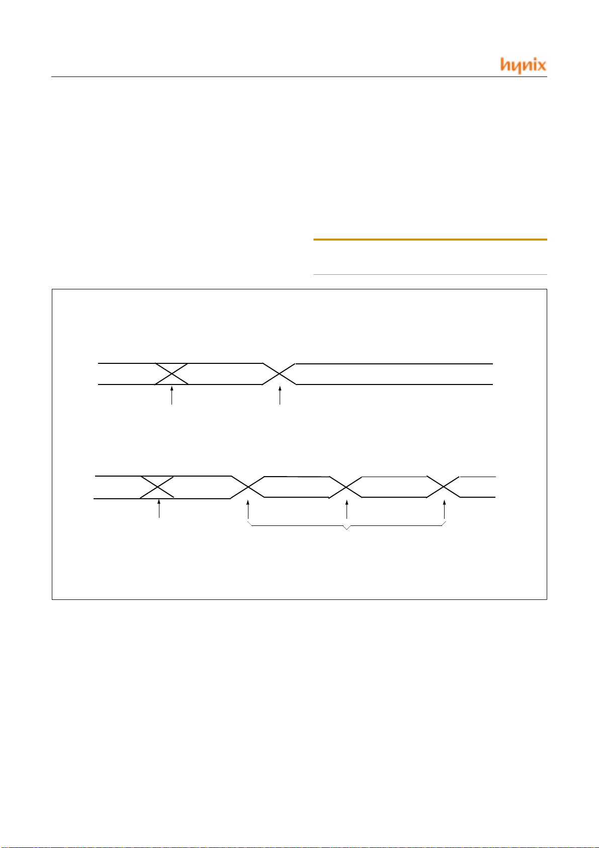
HMS81004E/08E/16E/24E/32E
3) Single/Modulo-N Mode
Timer0 (Timer1) can sel ect initial (T0INIT, T 1INIT of
TM01) output level of Timer Output port. If initial level is
“L”, Low-Data R egister value of T imer Data Re gister is
transferred to comparator an d T0OUT (T1OUT) is to be
“Low”, if initial level is High? High -Data Register is
transferred and to be “High”. Single Mode can be set by
Mode Select bit (T0MOD, T1MOD) of Timer Mode Register (TM0, TM1) to “1” When used as Single Mode, Timer counts up and compares with value of Data Register. If
the result is same, Time Out interrupt occurs and leve l
of Timer Output port togg le, then counter stops a s reset
state. When used as Modulo-N Mode, T0MOD (T1MOD)
[ Single Mode ]
8bit/16bit
counting
Timer Enable initial
value toggle
should be set “0”. Counter counts up until the value of
Data Register and occurs Time-out interrupt. The level of
Timer Output port toggle and repeats process of
counting the value which is selected in Data Register.
During Modulo-N Mode, If interrupt select bit (T0IFS,
T1IFS) of Mode Register is “0”, Interrupt occurs on every
Time-out. If it is “1”, Interrupt occurs every second timeout.
Note: Timer Output is toggled whenever time out happen
[ Module-N Mode ]
8bit/16bit
counting
Timer Enable initial
value toggle
Figure 13-8 Operation Diagram for Single/Modulo-N Mode
(4) Timer 2
Timer2 operates as a up-counter. The content of T2DR are
compared with the contents of up-counter. If a match is
found. Timer2 interrupt (IFT2) is generated and the upcounter is cleared to “00h”. Therefore, Timer2 executes
as a interval timer. Interrupt period is determined by the
count source clock for the Timer2 and content of T2DR.
Timer-output toggle
Int occurs (IFS=1) Each 2nd time out
Int occurs (IFS=0) when Time out
When T2ST is set to “1”, count value of Timer 2 is cleared
and starts counting-up. For clearing and starting the
Timer2. T2ST have to set to “1” after set to “0”. In order to
write a value directly into the T2DR, T2ST sh ould be set
to “0”. Count value of Timer2 can be read at any time.
46 JUNE 2001 Ver 1.00
Page 50
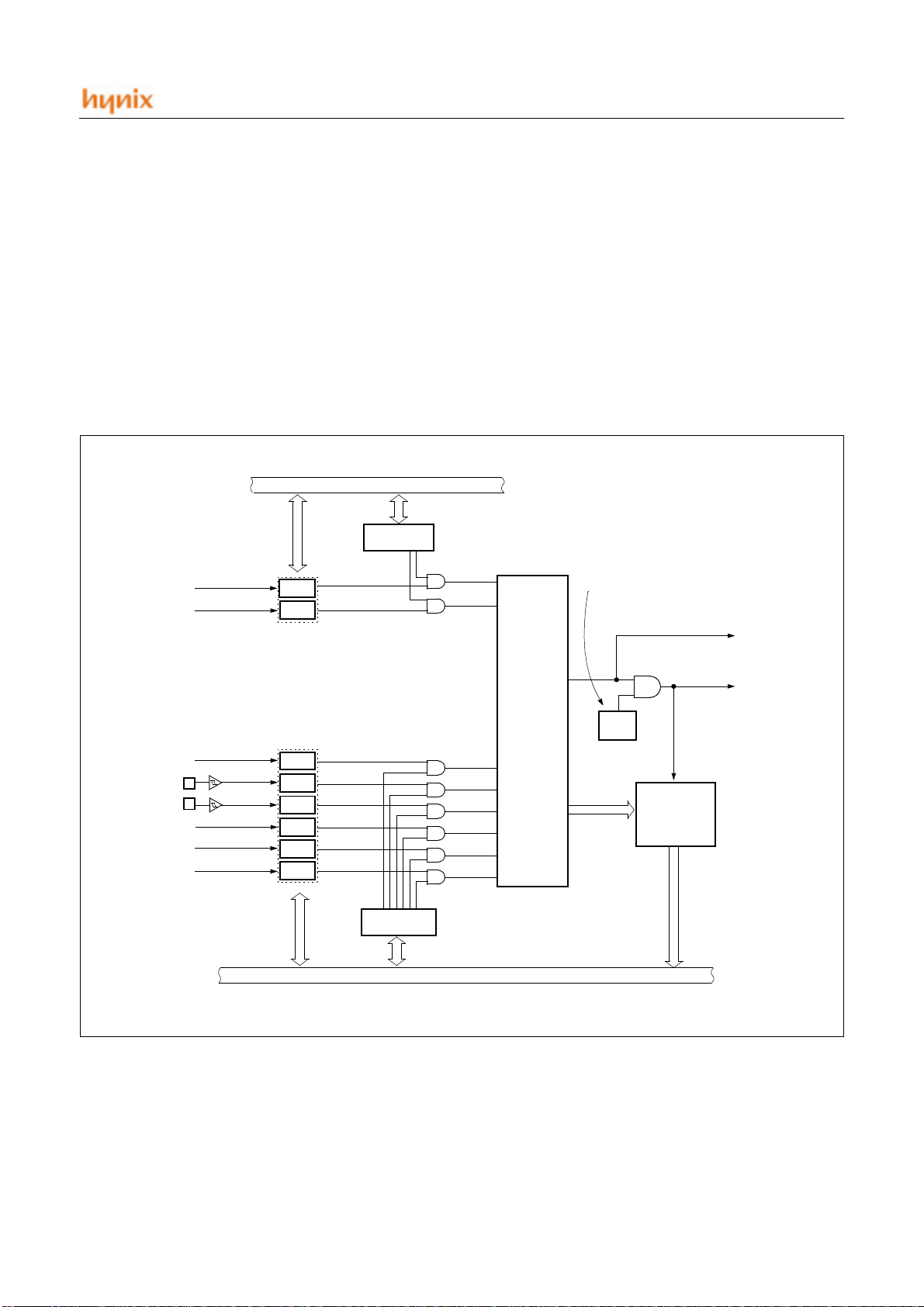
14. INTERRUPTS
HMS81004E/08E/16E/24E/32E
The HMS81004E/08E/16E/24E/32E interrupt circuits
consist of Interrupt Mode Register (M OD), Interrupt enable register (IENH, IENL), Interrupt request flags of
IRQH, IRQL, Priority circuit and Master enable flag ("I"
flag of PSW). 8 interrupt sources are provided. The config uration of interrupt circuit is shown in Figure 14-1 .
The HMS81004E/08E/16E/24E/3 2E contains 8 interrupt
sources; 3 externals and 5 internals. Nested interrupt services with priority control is also possible. Software interrupt is non-maskable interrupt, the others are all maskable
interrupts.
Internal bus line
IENL
IRQL
Watch Dog Timer
Basic Interval Timer
WDTR
BITR
- 8 interrupt source (2Ext, 3Timer, BIT, WDT and
Key Scan)
- 8 interrupt vector
- Nested interrupt control is possible
- Programmable interrupt mode
(Hardware and software interrupt accept mode)
- Read and write of interrupt request flag are possible.
- In interrupt accept, request flag is automatically cleared.
Interrupt Enable
Register (Lower byte)
I-flag is in PSW, it is cleared by “DI”, set by
“EI” instruction. When it goes interrupt service,
I-flag is cleared by hardware, thus any other
interrupt are inhibited. When interrupt service is
completed by “RETI” instruction, I-flag is set to
“1” by hardware.
Release STOP
Key Scan
INT1
INT2
Timer 0
Timer 1
Timer 2
IRQH
KSCNR
INT1R
INT2R
T0R
T1R
T2R
IENH
Internal bus line
Priority Control
Interrupt Enable
Register (Higher byte)
Interrupt Master
Enable Flag
Figure 14-1 Block Diagram of Interrupt
To CPU
I-flag
Interrupt
Vector
Address
Generator
JUNE 2001 Ver 1.00 47
Page 51
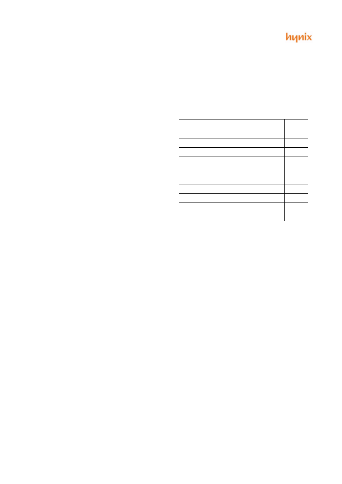
HMS81004E/08E/16E/24E/32E
14.1 Interrupt priority and sources
Each interrupt vector is independent and has its own priority. Software interrupt (BRK) is also availabl e. Interrupt
14.2 Interrupt control register
I flag of PSW is a interrupt mask enable flag. When I flag
= “0”, all interrupts become disable. When I flag = “1”, interrupts can be selectively enabled and disabled by contents of corresponding Interrupt Enable Register. When
interrupt is occured, interrupt request flag is set, and Interrupt request is detected at the edge of interrupt sig nal . The
accepted interru pt request flag is automatic ally cleared
during interrupt cycle process. The interrupt request flag
maintains “1” until the interrupt is accepted or is cleared in
program. In reset sta te, interrupt request flag regist er
(IRQH, IRQL) is cleared to “0”. It is possible to read the
state of interrupt register and to mainpulate the contents of
register and to generate interrupt. (Refer to software interrupt)
source classification is shown in Table 14-1.
Reset/Interrupt Symbol Priority
Hardware Reset RESET Key Scan KSCNR 1
External Interrupt1 INT1R 2
External Interrupt2 INT2R 3
Timer0 T0R 4
Timer1 T1R 5
Timer2 T2R 6
Watch Dog Timer WDTR 7
Basic Interval Timer BITR 8
BRK Instruction BRK -
Table 14-1 Interrupt Source
48 JUNE 2001 Ver 1.00
Page 52
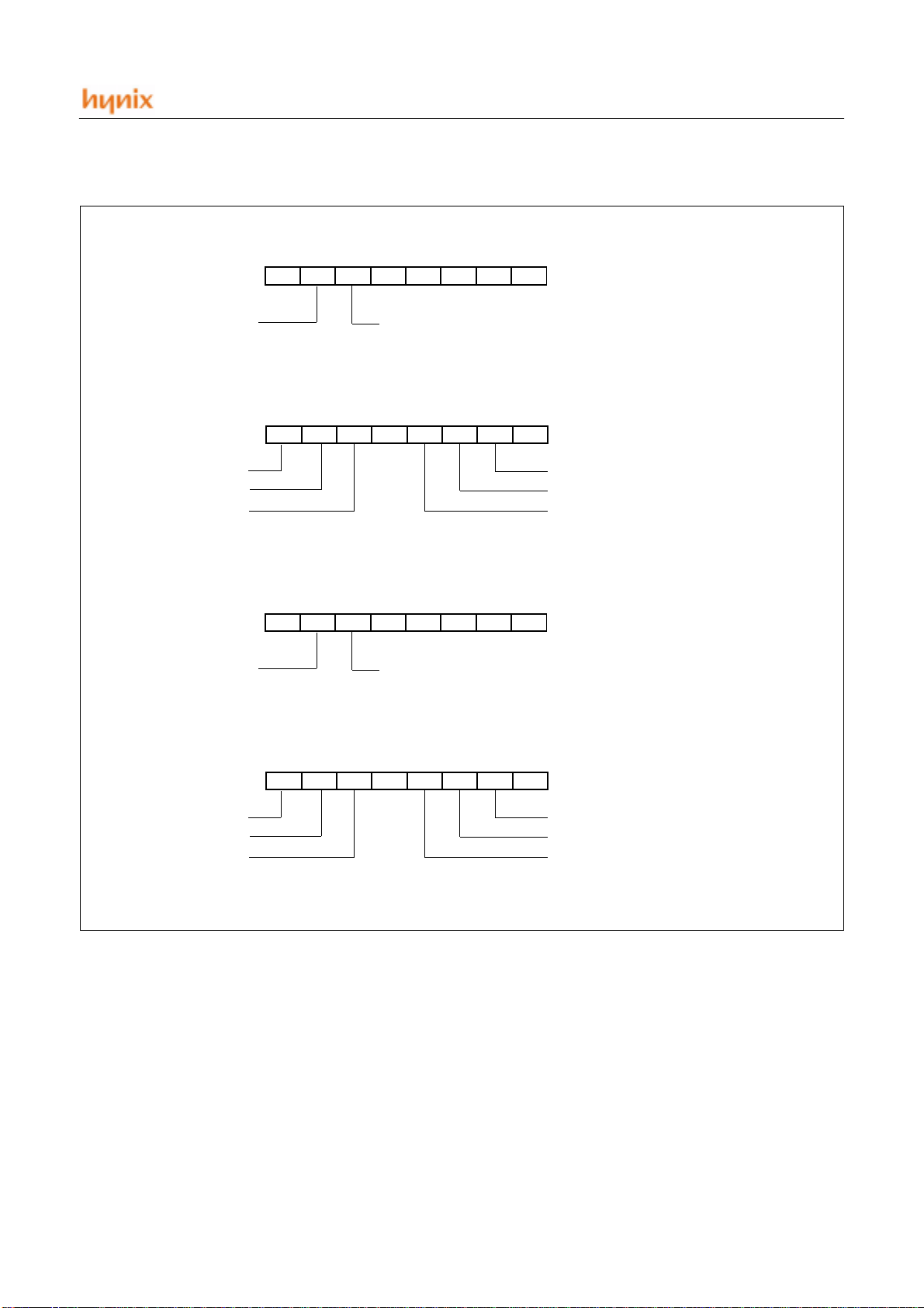
HMS81004E/08E/16E/24E/32E
R/WR/W
-
R/W
KSCNE
-
WDTE
INT1E
WDTR
R/WR/W
BITR
IENL
MSB LSB
IENH
MSB LSB
Key scan
External interrupt 1
External interrupt 2
.
IRQL
MSB LSB
-----BITE
Basic Interval TimerWatchdog timer
R/W
--
-----
Basic Interval TimerWatchdog timer
R/W R/WR/W R/W
T0E T1EINT2E
T2E
ADDRESS: 0CC
INITIAL VALUE: -00- ----
ADDRESS: 0CE
INITIAL VALUE: 000- 000-
Timer2
Timer1
Timer0
ADDRESS: 0CD
INITIAL VALUE: -00- ----
H
B
VALUE
H
B
H
B
0: Disable
1: Enable
IRQH
Key scan
External interrupt 1
External interrupt 2
R/W
KSCNR T2R
MSB LSB
INT1R
R/W
--
T0R T1RINT2R
Figure 14-2 Interrupt Enable & Request Flag
14.3 Interrupt accept mode
The interrupt priority order is determined by bit (IM1,
IM0) of IMOD register. The condition allow for accepting
interrupt is set state of the interrupt mask enable flag and
R/W R/WR/W R/W
ADDRESS: 0CF
INITIAL VALUE: 000- 000-
Timer2
Timer1
Timer0
H
B
the interrupt enable bit must be “1”. In Reset state, these
IP3 - IP0 registers become all “0”.
JUNE 2001 Ver 1.00 49
Page 53

HMS81004E/08E/16E/24E/32E
l
Interrupt mode register
IMOD
76543210
IM0
BTCL
IP 2IP3
IP1 IP0
--
IM1
ADDRESS: 0CA
INITIAL VALUE: --00_0000
R/W R/W R/W R/W R/W R/W
R/WR/W
H
B
Priority
00: Fixed by hardware
01: Changeable by IP3~IP0
1x: Interrupt is inhibited
Figure 14-3 Interrupt Accept Mode & Selection by IP3~IP0
14.4 Interrupt Sequence
An interrupt request is held until the interrupt is accepted or the
interrupt latch is cleared to “0” by a rese t or an instruc tio n. Interrupt acceptance sequ enc e re quire s 8
the current instruction exec ution. The in terrupt service task is terminated upon executio n of an interrup t return instr uction [RETI].
Interrupt acceptance
1. The interrupt master enable flag (I-flag) is cleared to
“0” to temporarily disable the acceptance of any following maskable interrupts. When a non-maskable interrupt is accepted, the acceptance of any following
interrupts is temporarily disabled.
after the completion of
f
XIN
Selection interrupt
0001: KSCNR
0010: INT1R
0011: INT2R
0101: T0R
0110: T1R
0111: T2R
1010: WDTR
1011: BITR
2. Interrupt request flag for the interrupt source accepted is
cleared to “0”.
3. The contents of the program counter (return address)
and the program status word are saved (pushed) onto the
stack area. The stack pointer decreases 3 times.
4. The entry address of the interrupt service program is
read from the vector table address and the entry address
is loaded to the program counter.
5. The instruction stored at the entry address of the interrupt service program is executed.
50 JUNE 2001 Ver 1.00
Page 54
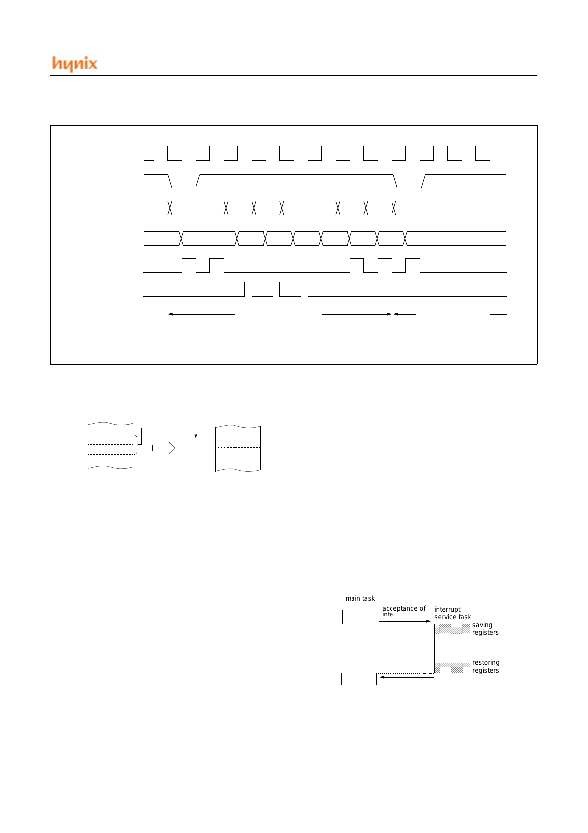
System clock
main task
interrupt
service task
saving
registers
restoring
registers
acceptance of
interrupt
interrupt return
Instruction Fetch
HMS81004E/08E/16E/24E/32E
Address Bus
Data Bus
PC
Not used
SP SP-1
PCH PCL
Internal Read
Internal Write
Interrupt Processing Step Interrupt Service Task
V.L. and V.H. are vector addresses.
ADL and ADH are start addresses of interrupt service routi ne as vector contents.
Figure 14-4 Timing chart of Interrupt Acceptance and Interrupt Return Instruction
External Interrupt1
Vector Table Address
012
0FFF8
H
0FFF9
H
Correspondence between vector table address for Exteranl Interrupt1
and the entry address of the interrupt service program.
0E3
H
H
0E312
0E313
Entry Address
0E
H
2E
H
H
H
A interrupt request is not accepted until t he I-flag is set to “1”
even if a requested interrupt has higher priority than that of the
current interrupt being serviced.
When nested interrupt service is required, the I-flag should be set
to “1” by “EI” instruction in the interrupt service program. In this
case, acceptable in terrupt sources are select ively enabled by the
individual interrupt enable flags.
SP-2 V.H. New PC
PSW ADL OP codeADH
V.L.
V.L.
registers.
Example: Registe r sa v e us in g pu s h an d po p ins t ru c tions
INTxx: PUSH A
PUSH X
PUSH Y
interrupt processing
POP Y
POP X
POP A
RETI
;SAVE ACC.
;SAVE X REG.
;SAVE Y REG.
;RESTORE Y REG.
;RESTORE X REG.
;RESTORE ACC.
;RETURN
General-purpose register save/restore using push and pop instructions;
Saving/Restoring General-purpose Register
During interrupt acceptance processing, the program counter and
the program status word are automatically saved on the stack, but
accumulator and other registers are not saved itsel f. These re gisters are saved by the software if necessary. Also, when multiple
interrupt services are nested, it is necessary to avoid using the
same data memory area for saving registers.
The following method is used to sav e/restore th e general-p urpose
JUNE 2001 Ver 1.00 51
Page 55
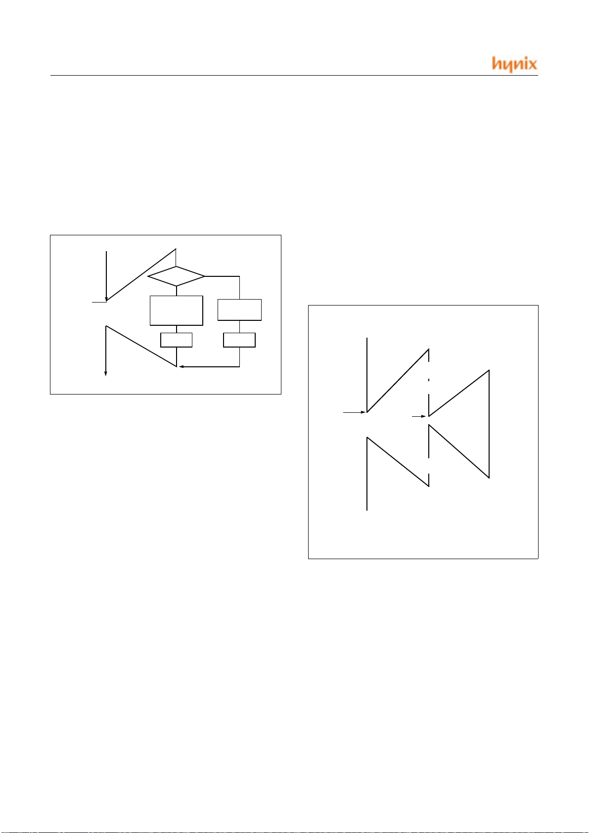
HMS81004E/08E/16E/24E/32E
enable INT1
TIMER 1
service
INT1
service
Main Program
service
Occur
TIMER1 interrupt
Occur
INT1
EI
disable other
enable INT1
enable other
In this example, the INT1 interrupt can be serviced without any
pending, even TIMER1 is in progress.
Because of re-setting the interrupt enable registers IENH,IENL
and master enable “EI” in the TIMER1 routine.
14.5 BRK Interrupt
Software interrupt can be invoked by BRK instru ction, whic h has
the lowest priority order.
Interrupt vector address of BRK is shared with the vector of
TCALL 0 (Refer to Program Memory Section). When BRK interrupt is generated, B-flag of PSW is set to distinguish BRK from
TCALL 0.
Each processing step is determined by B-flag as shown in Figure
14-5
=0
=1
TCALL0
ROUTINE
RET
BRK or
TCALL0
B-FLAG
BRK
INTERRUPT
ROUTINE
RETI
Example:
During Timer1 interrupt is in progress, INT1 inte rrupt
serviced without any suspend.
TIMER1: PUSH A
PUSH X
PUSH Y
LDM IENH,#40H ;
LDM IENL,#00H ;
EI ;
:
:
:
:
LDM IENH,#0FFH ;
LDM IENL,#0FFH
POP Y
POP X
POP A
RETI
Enable INT1 only
Disable other
Enable Interrupt
Enable all interrupts
Figure 14-5 Execution of BRK/TCALL0
14.6 Multi Interrupt
If two requests of different priority levels are received simultaneously, the request of higher priority level is serviced. If requests of the interrupt are received at the same time
simultaneously, an int ernal p olling sequ ence de termin es by hardware which request is serviced.
However, multiple processing through software for special features is possible. Generally when an interrupt is accepted, the Iflag is cleared to disable any further interrupt. But as user sets Iflag in interrupt routine, some further interrupt can be serviced
even if certain interrupt is in progress.
14.7 External Interrupt
) as
H
The external interrupt on INT1 and INT2 pins are edge triggere d
depending on the edge selection register IEDS (address 0D8
Figure 14-6 Execution of Multi Interrupt
shown in Figure14-7.
52 JUNE 2001 Ver 1.00
Page 56
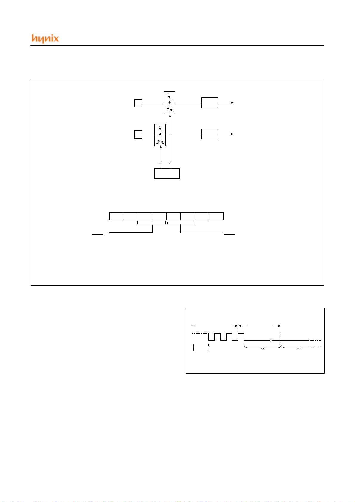
HMS81004E/08E/16E/24E/32E
Interrupt
goes
active
Interrupt
latched
Interrupt
processing
Interrupt
routine
8 f
XIN
periodmax. 12 f
XIN
period
Ext. Int. Edge Selection reg.
IEDS
IED2*
01: Falling Edge Selection
10: Rising Edge Selection
11: Both Edsg Selection
INT1 pin
INT2 pin
2 2
IEDS
[0CBH]
W
76543210
--
IED 2 H
WWW
BTCL
IED 2 L IE D 1 H IE D1 L
IFINT1
INT1 INTERRUPT
IFINT2
INT2 INTERRUPT
Edge selection
Register
-
ADDRESS: 0CB
INITIAL VALUE: 0000_0000
IED1*
01: Falling Edge Selection
10: Rising Edge Selection
11: Both Edsg Selection
H
B
Figure 14-7 External Interrupt Block Diagram
Response Time
The INT1 ~ INT2 edge are latched into IFINT1 ~ IFINT2 at every
machine cycle. The v alues are no t actu ally po lled by th e circuitry
until the next machine cycle. If a request is active and conditions
are right for it to be acknowledg e d, a hard ware sub r o uti ne call to
the requested service routine will be the next instructio n to be executed. The DIV itself takes twel ve cycles. T hus, a mini mum of
twelve complete machine cycles elapse between activation o f an
external interrupt request and the beginning of execution of the
first instruction of the service routine.
Figure 14-8 shows interrupt response timings.
14.8 Key Scan Input Processing
Key Scan Interrupt is generated by detectin g low or high
Input from each Input pin (R0, R1) is one of the sources
which release standby (SLEEP, STOP) mode. Key Scan
ports are all 16bit which are controlled by Standby Mode
Release Register (SMRR0, SMRR1). Key Input is considered as Interrupt, therefore, KSCNE bit of IEHN should be
Figure 14-8 Interrupt Response Timing Diagram
set for correct interrupt executing, SLEEP mode and STOP
mode, the rest of executing is the same as that of external
Interrupt. Each SMRR Register bit is allowed for each port
(for Bit= “0”, no Key Input, for Bit= “1”, Key Input available). At reset, SMRR becomes “00h”. So, there is no Key
Input source.
JUNE 2001 Ver 1.00 53
Page 57
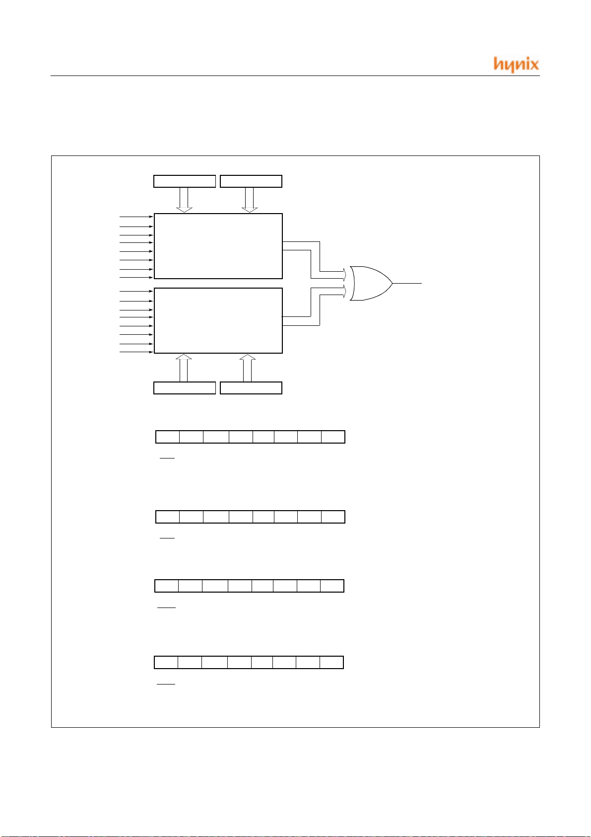
HMS81004E/08E/16E/24E/32E
Standby release level control register (SRLC) can select
the key scan input level “L” or “H” fo r stan dby release b y
each bit pin (R0, R1). Standby release level control register
SMRR0 SRLC0
R00
R01
R02
R03
R04
R05
R06
R07
R10
R11
R12
R13
R14
R15
R16
R17
R0 PORT LOGIC
R1 PORT LOGIC
SMRR1 SRLC1
(SRLC) is write-only register and initialized as “00h” in reset state.
Internal
Key Scan
Input
SMRR0
SMRR1
SRLC0
SRLC1
WW
76543210
KR07
KR06 KR05 KR04 KR03 KR02
KR0*
1: Select
0: No Select
WW
76543210
KR17
KR16 KR15 KR14 KR13 KR12
KR1*
1: Select
0: No Select
WW
76543210
KLR07
KLR06 KLR05 KLR04 KLR03 K LR02
KLR0*
1: High
0: Low
WW
76543210
KLR17
KLR16 KLR15 KLR14 KLR13 K LR12
KLR1*
1: High
0: Low
BTCL
BTCL
BTCL
BTCL
KLR11 KLR10
W
WWWWW
KR01 KR00
W
WWWWW
KR11 KR10
W
WWWWW
KLR0 1 KLR 00
W
WWWWW
ADDRESS: 0DC
INITIAL VALUE: 00
ADDRESS: 0DD
INITIAL VALUE: 00
ADDRESS: 0F6
INITIAL VALUE: 00
ADDRESS: 0 F7
INITIAL VALUE: 00
H
H
H
H
H
H
H
H
Figure 14-9 Block Diagram of Key Scan Block
54 JUNE 2001 Ver 1.00
Page 58
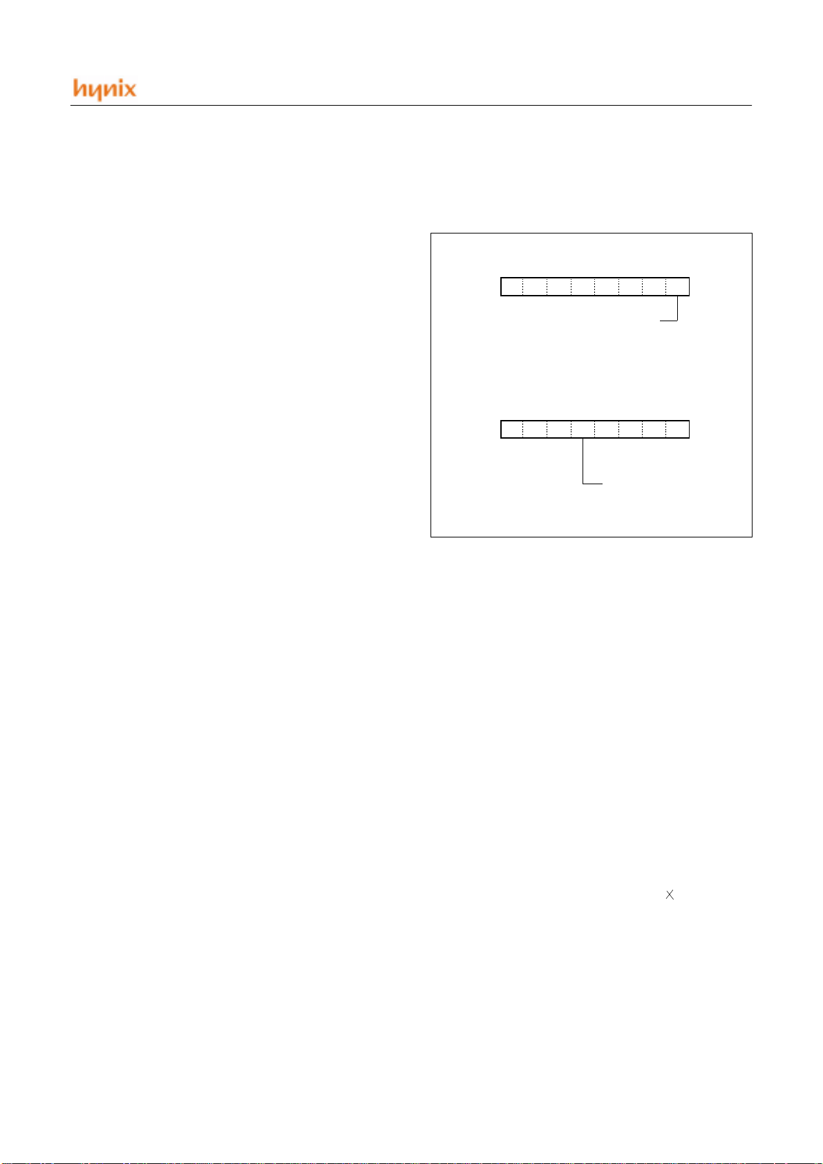
15. STANDBY FUNCTION
Sleep Mode Control Register (W)
SLPM
ADDRESS : 0F0
H
INITIAL VALUE : -------0b
-
SLPM0
1: sleep mode
Clock Control Register (W)
CKCTLR
ADDRESS : 0C7
H
INITIAL VALUE : --110111b
0
123
4567
ENPCK 0: Stopped
1: Provided
---- --
0: Sleep mode release
0
15.1 Sleep Mode
HMS81004E/08E/16E/24E/32E
SLEEP mode can be entered by setting the bit of SLEEP
mode register (SLPM). In the mode, CPU clock stops but
oscillator keeps running. B.I.T and a part of peripheral
hardware execute, but prescalerís output which provide
clock to peripherals can be stopped by program. (Except,
PS10 can’t stopped.) In SLEEP mode, more consuming
power can be saved by not using other peripheral hard ware
except for B.I.T. By setting ENPCK (peripheral clock control bit) of CKCTLR (clock control register) to “0”, peripheral hardware halted, and SLEEP mode is entered. To
release SLEEP mode by BITR (basic interval timer interrupt), bit10 of prescaler should be selected as B.I.T input
clock before entering SLEEP mode. “NOP” instruction
should be follows setting of SLEEP mode for risi ng pr echarge time of data bus line.
(ex) setting of SLEEP mode : set the bit of SLEEP
; mode register (SLPM)
NOP : NOP instruction
15.2 STOP MODE
STOP mode can be en tered by STOP instruction dur ing
program. In STOP mode, oscillator is stopped to make all
clocks stop, which leads to less power consumption. All
registers and RAM data are preserved. “NOP” instruction
should be follows STOP instruction for rising precharge
time of Data Bus line.
(ex) STOP : STOP instruction execution
NOP : NOP instruction
JUNE 2001 Ver 1.00 55
Page 59
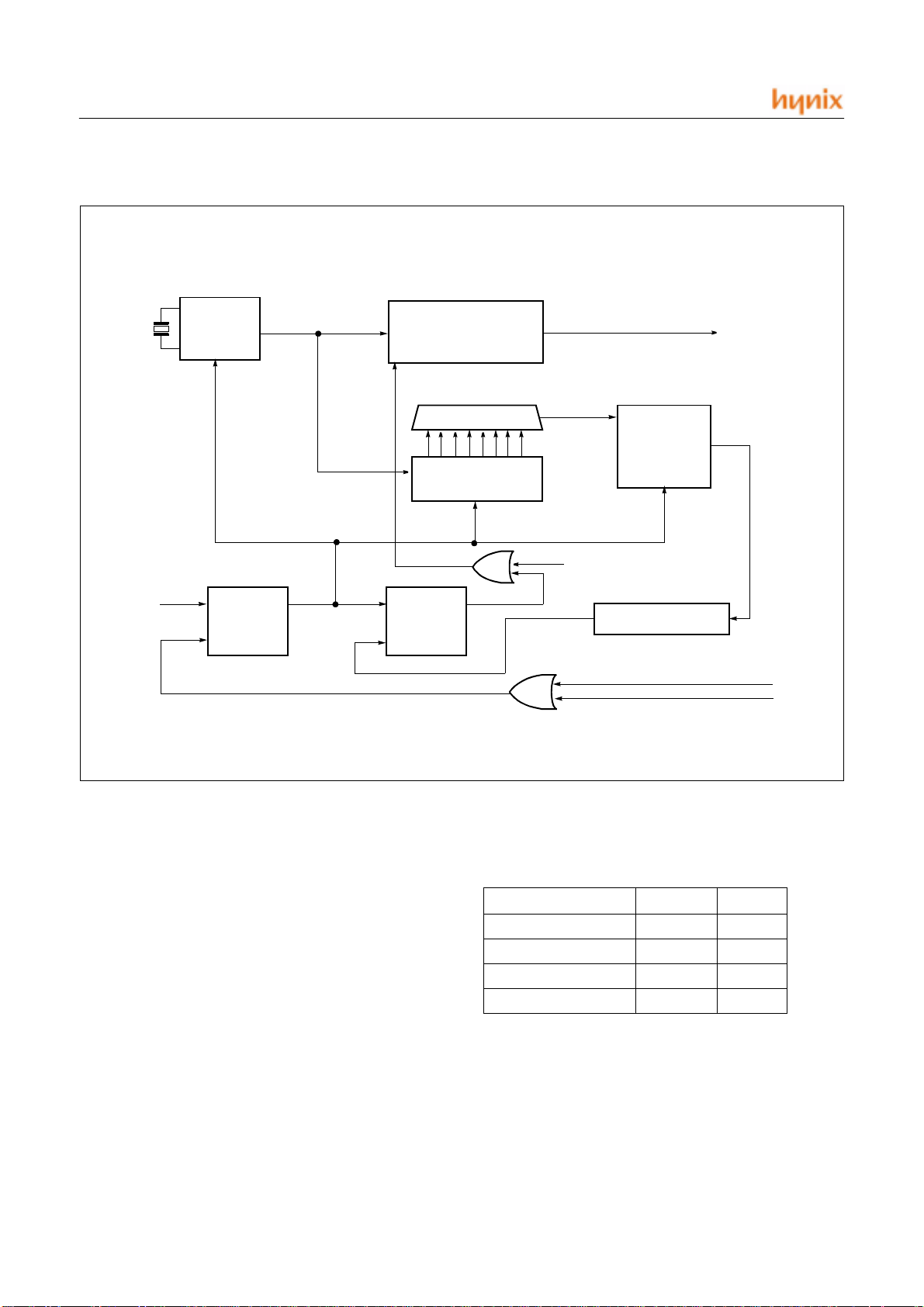
HMS81004E/08E/16E/24E/32E
STOP
OSC
Circuit
S
R
Clock Pulse
Generator
MUX
Basic
CPU Clock
Interval
Timer
Prescaler
Clear
Clear
bit7
Control Signal
Q
S
Q
Overflow Detection
R
Release Signal from Interrupt
RESETB
Figure 15-1 Block Diagram of Standby Circuit
15.3 STANDBY MODE RELEASE
Release of STANDBY mode is executed by RESET input
and Interrupt signal. Regist er value is defin ed when Reset.
When there is a release signal of STOP mode (Interrupt,
Release Signal SLEEP STOP
RESET input), the instruction execution starts after stabilization oscillation time is set by value of BTS2 ~ BTS0
and set ENPCK to “1”.
RESETB O O
KSCN(Key Input) O O
INT1,INT2 O O
B.I.T. O
Table 15-1 Release Signal of Standby Mode
56 JUNE 2001 Ver 1.00
Page 60
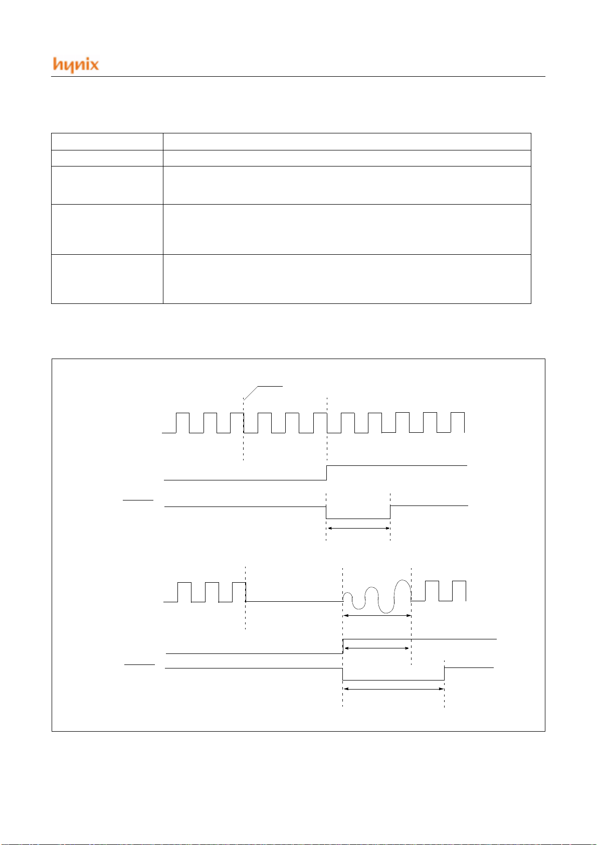
HMS81004E/08E/16E/24E/32E
Release Factor Release Method
RESETB By RESETB Pin=Low level, Standby mode is releas and system is initialized
Standby mode is released by low input of selected pin by key scan Input(SMRR0,SMRR1).
KSCN(Key Input)
INT1,INT2
Basic Interval
Timer(IFBIT)
In case of interrupt mask enable flag= “0”, program executes just after standby instruction,
if flag= “1” enters each interrupt service routine.
When external interrupt (INT1,INT2)enable flag is “1”, standby mode is released at the
rising edge of each terminal. When standby mode is released at interrupt. Mask Enable
flag= “0”, program executes from the next instruction of standby instruction. When “1”,
enters each interrupt service routine.
When B.I.T. is executed only by bit10 of prescaler(PS10), SLEEP mode can be released.
Interrupt release SLEEP mode , when BIT inte rrupt ena ble flag is “1”. Wh en stand by mode
is released at interrupt. Mask enable flag= “0”, program executes from the next instruction
of SLEEP instruction. When “1”, enters each interrupt service routine.
Table 15-2
[SLEEP MODE]
release by interrupt
[STOP MODE]
release by interrupt
Xin
RESET
Xin
RESET
SLEEP command
SLEEP mode
STOP mode
Longer than 2 machine cycle
Stable OSC.time
Program setting time by CKCTLR
Longer than stabe OSC. Time
Figure 15-2 Block Diagram of Standby Circuit
JUNE 2001 Ver 1.00 57
Page 61
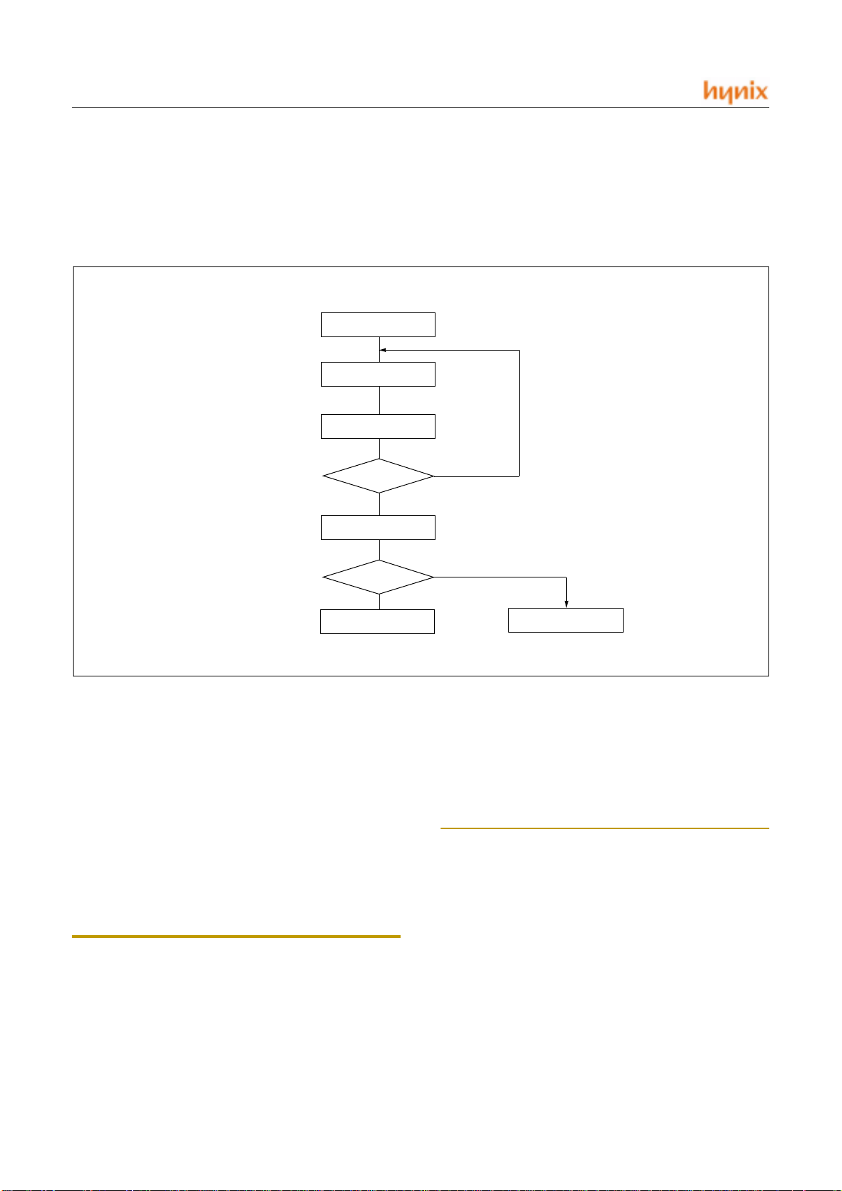
HMS81004E/08E/16E/24E/32E
15.4 RELEASE OPERA TION OF STANDBY MODE
After standby mode is released, the operation be gins according to content of related interrupt register just before
STOP Command
Standby Mode
Interrupt Request GEN.
Int. enable reg.
1
Standby Mode Release
PSW
I Flag
1
Interrupt Service Routine
standby mode start (Figure 15-3).
0
0
Standby Next Command
Execution
.
Figure 15-3 Standby Mode Release Flow
(1) Interrupt Enable Flag(I) of PSW = “0”
Release by only interrupt which interrupt enable flag =
“1”, and starts to execute from next to standby instruction
(SLEEP or STOP).
(2) Interrupt Enable Flag(I) of PSW = “1”
Released by only interrupt which each interrupt enable flag
= “1”, and jump to the relevant interrupt service routine.
Note: When STOP instruction is used, B.I.T should guarantee the stabilizati on oscillati on time. Thus, jus t before en-
tering STOP mode, clock of bit10 (PS10 ) of prescale r is
selected or peripheral hardware clock control bit (ENPCK)
to “1”, Therefore the clock necessary for stabilization oscillation time should be input into B.I.T. otherwise, standby
mode is released by reset signal. In case of interrupt request flag and interrupt enable flag are both “1”, standby
mode is not entered.
58 JUNE 2001 Ver 1.00
Page 62
HMS81004E/08E/16E/24E/32E
Internal circuit SLEEP mode STOP mode
Oscillator Active Stop
Internal CPU Stop Stop
Register Retained Retained
RAM Retained Retained
I/O port Retained Re tai ned
Prescaler Active Retained
Basic Interval Timer
Watch-dog Timer Stop Stop
Timer Stop Stop
Address Bus,Data Bus Retained Retained
Table 15-3 Operation State in Standby Mode
PS10 select ed:Active
Others: Stop
Stop
JUNE 2001 Ver 1.00 59
Page 63
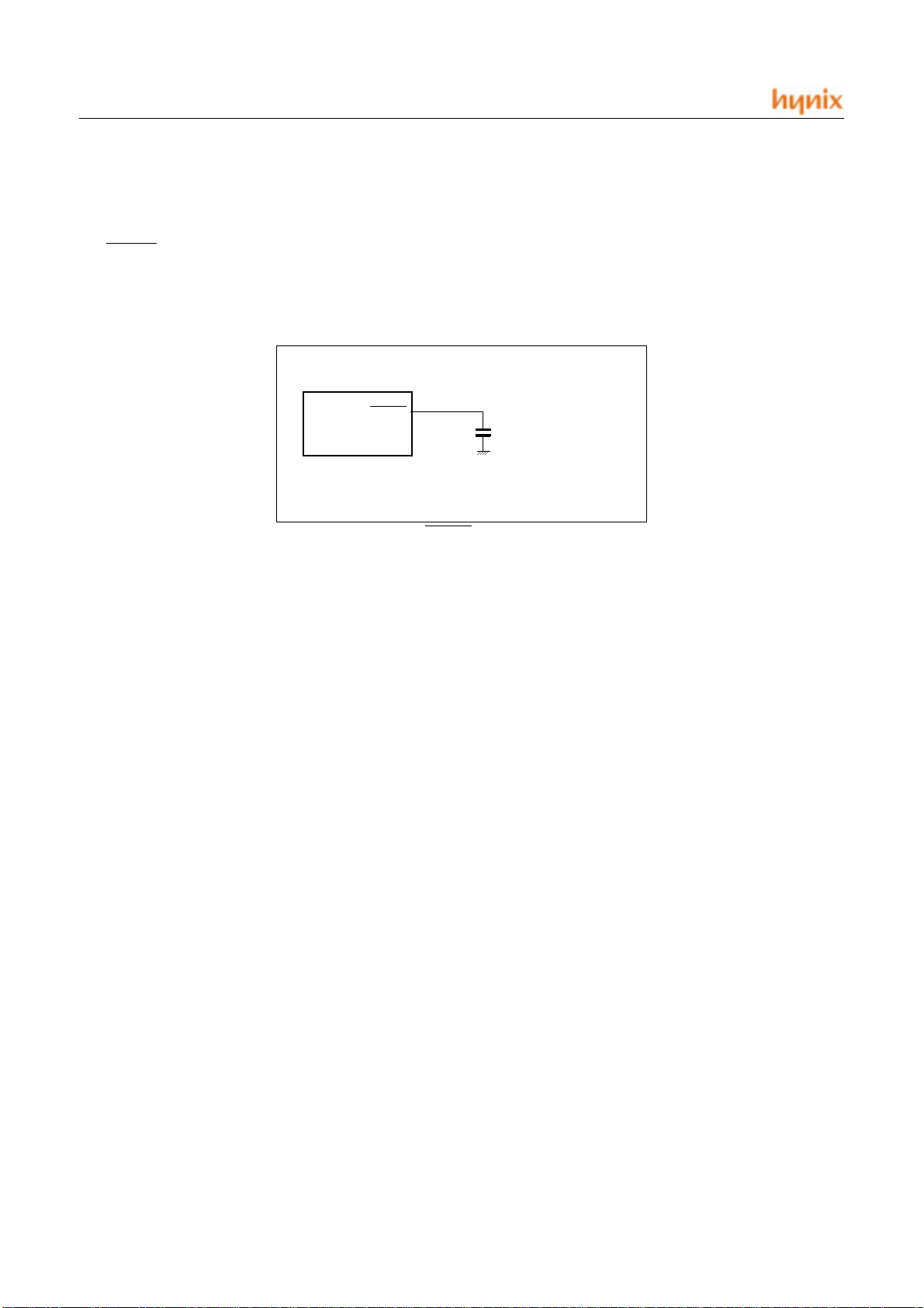
HMS81004E/08E/16E/24E/32E
16. RESET FUNCTION
16.1 EXTERNAL RESET
The RESET pin should be held at low for at least 2mach ine
cycles with the power supply voltage within th e operat ing
voltage range and must be connected 0.1uF capacitor for
RESET
Figure 16-1 RESET Pin connection
16.2 POWER ON RESET
Power On Reset circuit automatically detects the rise of
power voltage (the rising time s hould be with in 50ms ) the
power voltage reaches a certain level, RESET terminal is
maintained at “L” Level until a crystal ceramic oscillator
oscillates stably. After power applies and starting of oscillation, this reset state is maintained for about oscillation
cycle of 219 (about 65.5ms : at 4MHz).The execution of
built-in Power On Reset circuit is as follows :
(1) Latch the pulse f rom Power On Detection Pu lse Generator circuit, and reset Prescaler, B.I.T and B.I.T Overflow
stable system initialization. The RESET pin contains a
Schmitt trigger with an internal pull-up resistor.
0.1uF capacito r
GND
detection circuit.
(2) Once B.I.T Overflow detection circuit is reset. Then,
Prescaler starts to count.
(3) Prescaler output is inputted into B.I.T and PS10 of
Prescaler output is automatically selected. If overflow of
B.I.T is detected, Overflow detection circuit is set.
4) Reset circuit generates maximum period of reset pulse
from Prescaler and B.I.T
60 JUNE 2001 Ver 1.00
Page 64
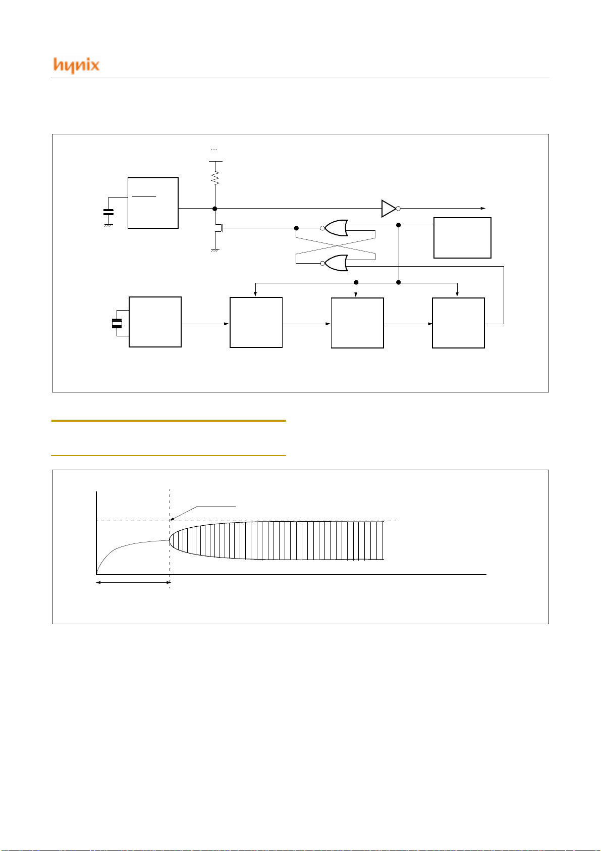
HMS81004E/08E/16E/24E/32E
VDD
RESET
0.1uF
GND
GND
Clear
OSC
Circuit
Prescaler
Figure 16-2 Block Diagram of Power On Reset Circuit
Note: When Power On Reset, oscillator stabilization time
doesn`t include OSC. Start time.
VDD
Prescaler Count Start
PS10
Internal Reset
Power on
Detect Pulse
Generator
Clear
Basic
Interval
Timer
MSB
Clear
B.I.T.
Overflow
Detction
Circuit
OSC. Start Time
Figure 16-3 Oscillator stabiliaztion diagram
JUNE 2001 Ver 1.00 61
Page 65
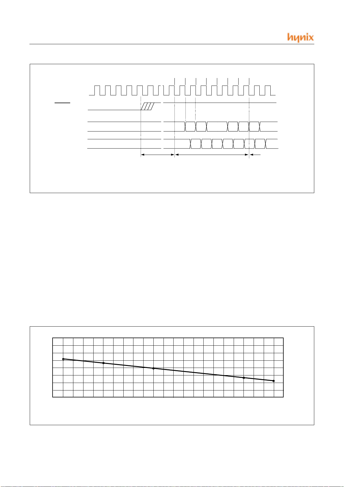
HMS81004E/08E/16E/24E/32E
Oscillator
(X
pin)
IN
RESET
ADDRESS
BUS
DATA
BUS
ADL and ADH are start addresses of interrupt service routine as vector contents.
?
?
Stabilization Time
Figure 16-4 Timing Diagram of Reset
16.3 Low Voltage Detection Mode
(1) Low voltage detection condition
An on board voltage comparator checks that VDD is at the
required level to ensure correct operation of the device. If
VDD is below a certain level, Low voltage detector forces
the device into low voltage detection mode.
~
~
~
~
~
~
~
~
~
~
~
~
1 2 3 4 5 6 7
?
??
??
RESET Process Step
FFFE FFFF
FE?ADL
ADH
Start
OP
MAIN PROGRAM
all port can be selected with Pull-up resistor by Mask option. If there is no information on the Mask option sheet
,the default pull up option (all port connect to pull-up resistor ) is selected.
(3) Release of Low Voltage Detection Mode
(2) Low Voltage Detection Mode
There is no power consumption except stop current, stop
mode release function is disabled. All I/O port is configured as input mode and Data memory is retained until voltage through external capacitor is worn out. In this mode,
LVD(V)
1.85
1.80
1.75
1.70
1.65
1.60
1.55
-25 -20 -15 -10 -5 0 5 10 15 20 25 30 35 40 45 50 55 60 65 70 75 80 85 90
Temperature (
Figure 16-5 Low Voltage vs Temperature
Reset signal result from new battery(normally 3V) wakes
the low voltage detection mode and come into normal reset
state. It depends on user whether to execute RAM clear
routine or not
C)
°
62 JUNE 2001 Ver 1.00
Page 66
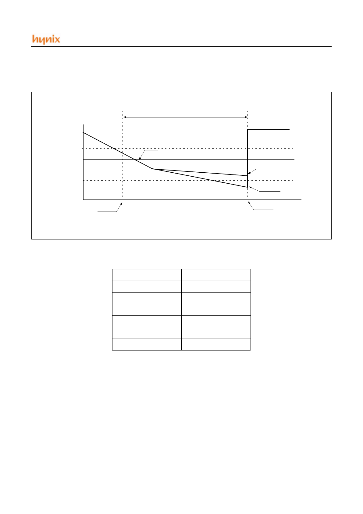
(4) SRAM BACK-UP after Low Voltage Detection.
about hours depend on Vdd-GND Capacito r
VDD
3V
SRAM Dat a Backup
HMS81004E/08E/16E/24E/32E
2V(Min.)
1.7V(typ.20 °
0.7V(Vret)
C
)
0V
User removes
batteries
Low Voltage detetion point
Power on Reset
(SRAM retention)
Power on Reset
(SRAM unstable)
Time
User replac es
batteries
Figure 16-6 Oscillator stabiliaztion diagram
Interrupt disable
Stop release disable
All I/O port input Mode
Remout port Low Level
OSC STOP
All I/O port pull-up on Mask Option
SRAM Data retention until Vret
Table 16-1 The operation after Low Voltage detection
JUNE 2001 Ver 1.00 63
Page 67
HMS81004E/08E/16E/24E/32E
(5) S/W flow chart example after Reset using SRAM Back-up
RESET
Stack Pointer initialize
Check the SRAM value
(RAM Pattern, Checksum)
SRAM DATA
VALID?
Y
Use Saved SRAM value
Main routine
N
Clear all Ram area
Figure 16-7 S/W flow chart example after Reset using SRAM Back-up
64 JUNE 2001 Ver 1.00
Page 68

APPENDIX
Page 69
A. MASK ORDER SHEET
MASK ORDER & VERIFICATION SHEET
HMS810
E -UE
Customer should write inside thick line box.
1. Customer Information
Company Name
Application
Order Date
Tel:
Name&Signature:
YYYY MM DD
Fax:
2. Device Information
20SOP
Package
Mask Data File Name: ( .OTP)
Check Sum ( @27c256)
24SOP
28SOP
28PIN DIE
3. Inclusion of pull-up resistor in Low Volatage Detection mode
*1
Port R00 R01 R02 R03 R04
Y/N
*1 : is not avilable for 20PIN. So default option is pull-up on.
*2 : is not avilable for 20PIN & 24PIN. So default option is pull-up on.
R05 R06
R07
R10 R11 R12 R13 R14
*1 *1 *1
R15 R16
R17
*2
R20 R21 R22 R23 R24
4. Marking Specification
(Please check mark into )
20PDIP
24SKDIP
28SKDIP
*2
*2 *2
04/08/16/24/32
Customer’s logo
HMS810
E -UE
Hynix ROM Code
Number
HMS810
YYWW
If the customer logo must be used in the special mark, please submit a clean original of the logo.
Customer’s part number
KOREA
Lot Number
YYWW
Customer logo is not required.
5. Delivery Schedule
Customer Sample
Risk Order
YYYY MM DD
YYYY MM DD
6. ROM Code Verification
Verifica tio n D a te :
Please confirm our verification data.
Check Sum:
Tel: Fax:
Name &
Signature:
YYYY MM DD
Date
Quantity
pcs
pcs
This box is written after “6.Verification”.
Approval Date:
I agree with your verification data and confirm
yo u to m a k e ma sk se t.
Tel:
Name &
Signature:
E -UE
KOREA
Hynix Confirmation
YYYY MM DD
Fax:
JUNE 2001
Page 70
B. INSTRUCTION
B.1 Terminology List
Terminology Description
A Accumulator
X X - register
Y Y - register
PSW Program Status Word
#imm 8-bit Immediate data
dp Direct Page Offset Address
!abs Absolute Address
[ ] Indirect expr ession
{ } Register Indirect expression
{ }+ Register Indirect expression, after that, Register auto-increment
.bit Bit Position
A.bit Bit Position of Accumulator
dp.bit Bit Position of Direct Page Memory
M.bit
rel Relative Addressing Data
upage
n Table CALL Number (0~15)
+ Addition
x
y
−
×
/ Division
( ) Contents Expression
∧
∨
⊕
~NOT
←
→
↔
= Equal
≠
Bit Position of Memory Data (000
~0FFFH)
H
U-page (0FF00H~0FFFFH) Offset Address
0
Bit Position
1
Bit Position
Upper Nibble Expression in Opcode
Upper Nibble Expression in Opcode
Subtraction
Multiplication
AND
OR
Exclusive OR
Assignment / Transfer / Shift Left
Shift Right
Exchange
Not Equal
APPENDIX
JUNE 2001 Ver 1.00 lxxi
Page 71

APPENDIX
B.2 Instruction Map
0000000000010100010020001103001000400101050011006001110701000080100109010100A010110B011000C011010D011100E01111
LOW
HIGH
0F
000 -
001 CLRC
010 CLRG
011 DI
100 CLRV
101 SETC
110 SETG
111 EI
LOW
HIGH
000
SET1
dp.bit
1000010100011110010121001113101001410101151011016101111711000181100119110101A110111B111001C111011D111101E11111
BPL
CLR1
rel
dp.bit
BBS
A.bit,rel
BBC
A.bit,rel
BBS
dp.bit,rel
BBC
dp.bit,rel
ADC
ADCdpADC
#imm
SBC
#imm
CMP
#imm
OR
#immORdpORdp+XOR!abs
AND
#imm
EOR
#imm
LDA
#imm
LDM
dp,#imm
ADC
{X}
!abs+Y
dp+X
SBCdpSBC
dp+X
CMPdpCMP
dp+X
ANDdpAND
dp+X
EORdpEOR
dp+X
LDAdpLDA
dp+X
STAdpSTA
dp+X
ADC
ADC
[dp+X]
ADC
!abs
SBC
!abs
CMP
!abs
AND
!abs
EOR
!abs
LDA
!abs
STA
!abs
ADC
[dp]+Y
ASLAASLdpTCALL0SETA1
ROLAROLdpTCALL2CLRA1
LSRALSRdpTCALL4NOT1
RORARORdpTCALL6OR1
INCAINCdpTCALL8AND1
DECADECdpTCALL10EOR1
LDYdpTCALL12LDC
TXA
STYdpTCALL14STC
TAX
ASL
ASL
dp+X
TCALL1JMP
!abs
.bit
.bit
M.bit
OR1B
AND1B
EOR1B
LDCB
M.bit
!abs
BITdpPOPAPUSH
COMdpPOPXPUSHXBRA
TSTdpPOPYPUSHYPCALL
CMPXdpPOP
CMPYdpCBNE
DBNEdpXMA
LDXdpLDX
STXdpSTX
BIT
ADDWdpLDX
!abs
PSW
dp+X
dp+X
dp+Y
dp+Y
PUSH
TXSP
TSPX
#imm
BRK
A
rel
Upage
RET
PSW
INC
X
DEC
X
XCN DAS
XAX STOP
1F
JMP
[!abs]
001
010
011
100
101
110
111
BVC
rel
BCC
rel
BNE
rel
BMI
rel
BVS
rel
BCS
rel
BEQ
rel
SBC
SBC
SBC
CMP
AND
EOR
LDA
STA
SBC
[dp]+Y
CMP
[dp]+Y
AND
[dp]+Y
EOR
[dp]+Y
LDA
[dp]+Y
STA
[dp]+Y
{X}
!abs+Y
[dp+X]
CMP
CMP
{X}
!abs+Y
[dp+X]
OR
{X}OR!abs+YOR[dp+X]OR[dp]+Y
AND
AND
{X}
!abs+Y
[dp+X]
EOR
EOR
{X}
!abs+Y
[dp+X]
LDA
LDA
{X}
!abs+Y
[dp+X]
STA
STA
{X}
!abs+Y
[dp+X]
ROL
!abs
LSR
!abs
ROR
!abs
INC
!abs
DEC
!abs
LDY
!abs
STY
!abs
ROL
TCALL3CALL
dp+X
LSR
TCALL
dp+X
ROR
dp+X
INC
dp+X
DEC
dp+X
LDY
dp+X
STY
dp+X
5
TCALL7DBNEYCMPX
TCALL
9
TCALL11XMA
TCALL13LDA
TCALL15STA
TEST
!abs
!abs
TCLR1
MUL
!abs
!abs
CMPY
DIV
!abs
XMAdpDECWdpDEC
{X}
LDX
{X}+
!abs
STX
{X}+
!abs
SUBWdpLDY
CMPWdpCMPX
#imm
#imm
LDYAdpCMPY
#imm
INCWdpINC
STYA
dp
CBNE
dp
Y
Y
XAY DAA
XYX NOP
JMP
[dp]
CALL
[dp]
RETI
TAY
TYA
lxxii JUNE 2001 Ver 1.00
Page 72
B.3 Instruction Set
Arithmetic / Logic Operation
APPENDIX
No. Mnemonic
1 ADC #imm 04 2 2 Add with carry.
2 ADC dp 05 2 3 A ← ( A ) + ( M ) + C
3 ADC dp + X 06 2 4
4 ADC !abs 07 3 4
5 ADC !abs + Y 15 3 5
6 ADC [ dp + X ] 16 2 6
7 ADC [ dp ] + Y 17 2 6
8 ADC { X } 14 1 3
9 AND #imm 84 2 2 Logical AND
10 AND dp 85 2 3 A ← ( A ) ∧ ( M )
11 AND dp + X 86 2 4
12 AND !abs 87 3 4
13 AND !abs + Y 95 3 5
14 AND [ dp + X ] 96 2 6
15 AND [ dp ] + Y 97 2 6
16 AND { X } 94 1 3
17 ASL A 08 1 2
18 ASL dp 09 2 4
19 ASL dp + X 19 2 5
20 ASL !abs 18 3 5
21 CMP #imm 44 2 2
22 CMP dp 45 2 3
23 CMP dp + X 46 2 4
24 CMP !abs 47 3 4
25 CMP !abs + Y 55 3 5
26 CMP [ dp + X ] 56 2 6
27 CMP [ dp ] + Y 57 2 6
28 CM P { X } 54 1 3
29 CMPX #imm 5E 2 2 Compare X conte nts with memory contents
30 CM PX dp 6C 2 3 ( X ) - ( M )
31 CMPX !abs 7C 3 4
32 CMPY #imm 7E 2 2 Compare Y conte nts with memory contents
33 CM PY dp 8C 2 3 ( Y ) - ( M )
34 CMPY !abs 9C 3 4
35 COM dp 2C 2 4 1’S Complement : ( dp ) ← ~( dp )
36 DAA DF 1 3 Decimal adjust for addition
37 DAS CF 1 3 Decimal adjust for subtraction
38 DEC A A8 1 2 Decrement
39 DEC dp A9 2 4 M ← ( M ) - 1
40 DEC dp + X B9 2 5
41 DEC !abs B8 3 5
42 DEC X AF 1 2
43 DEC Y BE 1 2
Op
Code
ByteNoCycle
No
Operation
Arithmetic shift left
76543210
C
←
Compare accumulator contents with memory contents
( A ) - ( M )
“0”
←
←←←←←←←←
Flag
NVGBHIZC
NV--H-ZC
N-----Z-
N-----ZC
N-----ZC
N-----ZC
N-----ZC
N-----ZN-----ZC
N-----ZC
N-----ZN-----ZN-----ZN-----ZN-----ZN-----Z-
JUNE 2001 Ver 1.00 lxxiii
Page 73
APPENDIX
No. Mnemonic
Op
Code
ByteNoCycle
No
Operation
44 DIV 9B 1 12 Divide : YA / X Q: A, R: Y
45 EOR #imm A4 2 2 Exclusive OR
46 EOR dp A5 2 3 A ← ( A ) ⊕ ( M )
47 EOR dp + X A6 2 4
48 EOR !abs A7 3 4
49 EOR !abs + Y B5 3 5
50 EOR [ dp + X ] B6 2 6
51 EOR [ dp ] + Y B7 2 6
52 EOR { X } B4 1 3
53 INC A 88 1 2 Increment
54 INC dp 89 2 4 M ← ( M ) + 1
55 INC dp + X 99 2 5
56 INC !abs 98 3 5
57 INC X 8F 1 2
58 INC Y 9E 1 2
59 LSR A 48 1 2
60 LSR dp 49 2 4
61 LSR dp + X 59 2 5
Logical shift right
76543210
“0”
→
62 LSR !abs 58 3 5
63 MUL 5B 1 9 Multiply : YA ← Y × A
64 OR #imm 64 2 2 Logical OR
65 OR dp 65 2 3 A ← ( A ) ∨ ( M )
66 OR dp + X 66 2 4
67 OR !abs 67 3 4
68 OR !abs + Y 75 3 5
69 OR [ dp + X ] 76 2 6
70 OR [ dp ] + Y 77 2 6
71 OR { X } 74 1 3
72 ROL A 28 1 2
73 ROL dp 29 2 4
Rotate left through Carry
76543210
C
74 ROL dp + X 39 2 5
75 ROL !abs 38 3 5
76 ROR A 68 1 2
77 ROR dp 69 2 4
Rotate right through Carry
76543210
78 ROR dp + X 79 2 5
79 ROR !abs 78 3 5
80 SBC #imm 24 2 2 Subtract with Carry
81 SBC dp 25 2 3 A ← ( A ) - ( M ) - ~( C )
82 SBC dp + X 26 2 4
83 SBC !abs 27 3 4
84 SBC !abs + Y 35 3 5
85 SBC [ dp + X ] 36 2 6
86 SBC [ dp ] + Y 37 2 6
87 SBC { X } 34 1 3
88 TST dp 4C 2 3
89 XCN CE 1 5
Test memory contents for negative or zero, ( dp ) - 00
Exchange nibbles within the accumulator
↔ A3~A
A
7~A4
0
Flag
NVGBHIZC
NV--H-Z-
N-----Z-
N-----ZC
N-----ZN-----ZN-----ZN-----ZN-----Z-
H
N-----ZC
N-----Z-
N-----Z-
N-----ZC
N-----ZC
NV--HZC
N-----Z-
N-----Z-
C
→→→→→→→→
→
←←←←←←←←
C
→→→→→→→→
lxxiv JUNE 2001 Ver 1.00
Page 74
Register / Memory Operation
APPENDIX
No. Mnemonic
1 LDA #imm C4 2 2 Load accumulator
2 LDA dp C5 2 3 A ← ( M )
3 LDA dp + X C6 2 4
4 LDA !abs C7 3 4
5 LDA !abs + Y D5 3 5
6 LDA [ dp + X ] D6 2 6
7 LDA [ dp ] + Y D7 2 6
8 LDA { X } D4 1 3
9 LDA { X }+ DB 1 4 X- register auto-increment : A ← ( M ) , X ← X + 1
10 LDM dp,#imm E4 3 5 Load memory with immediate data : ( M ) ← imm
11 LDX #imm 1E 2 2 Load X-register
12 LDX dp CC 2 3 X ← ( M )
13 LDX dp + Y CD 2 4
14 LDX !abs DC 3 4
15 LDY #imm 3E 2 2 Load Y-register
16 LDY dp C9 2 3 Y ← ( M )
17 LDY dp + X D9 2 4
18 LDY !abs D8 3 4
19 STA dp E5 2 4 Store acc umulator contents in memory
20 S TA dp + X E 6 2 5 ( M ) ← A
21 STA !abs E7 3 5
22 STA !abs + Y F5 3 6
23 STA [ dp + X ] F6 2 7
24 STA [ dp ] + Y F7 2 7
25 STA { X } F4 1 4
26 STA { X }+ FB 1 4 X- register auto-increment : ( M ) ← A, X ← X + 1
27 STX dp EC 2 4 Store X-register contents in memory
28 S TX dp + Y ED 2 5 ( M ) ← X
29 STX !abs FC 3 5
30 STY dp E 9 2 4 Store Y-register contents in memory
31 S TY dp + X F9 2 5 ( M ) ← Y
32 STY !abs F8 3 5
33 TAX E8 1 2 Transfer accumulator contents to X-register : X ← A
34 TAY 9F 1 2 Transfer accumulator contents to Y-register : Y ← A
35 TSPX AE 1 2 Transfer stack-pointer contents to X-register : X ← sp
36 TXA C8 1 2 Transfer X-register contents to accumulator: A ← X
37 TXS P 8E 1 2 Transfer X-re gister content s to stack-pointer: sp ← X
38 TYA BF 1 2 Transfer Y-register contents to accumulator: A ← Y
39 XAX EE 1 4 Exchange X-register contents with accumulator :X ↔ A
40 XAY DE 1 4 Exchange Y-register contents with accumulator :Y ↔ A
41 XMA dp BC 2 5 Exchange memory contents with accumulator
42 X MA dp+X AD 2 6 ( M ) ↔ A
43 X MA {X} BB 1 5
44 XYX FE 1 4 Exchange X-register contents with Y-register : X ↔ Y
Op
Code
ByteNoCycle
No
Operation
Flag
NVGBHIZC
N-----Z-
--------
N-----Z-
N-----Z-
--------
--------
--------
N-----ZN-----ZN-----ZN-----ZN-----ZN-----Z-
--------
--------
N-----Z-
--------
JUNE 2001 Ver 1.00 lxxv
Page 75
APPENDIX
16-BIT operation
No. Mnemonic
1 ADDW dp 1D 2 5
2CMPW dp 5D 2 4
3DECW dp BD 2 6
4 INCW dp 9D 2 6
5 LDYA dp 7D 2 5
6 STYA dp DD 2 5
7 SUBW dp 3D 2 5
Op
Code
ByteNoCycle
No
Operation
16-Bits add without Carry
YA ← ( YA ) ( dp +1 ) ( dp )
Compare YA contents with memory pair contents :
(YA) − (dp+1)(dp)
Decrement memory pair
( dp+1)( dp) ← ( dp+1) ( dp) - 1
Increment memory pair
( dp+1) ( dp) ← ( dp+1) ( dp ) + 1
Load YA
YA ← ( dp +1 ) ( dp )
Store YA
( dp +1 ) ( dp ) ← YA
16-Bits subtract without carry
YA ← ( YA ) - ( dp +1) ( dp)
Bit Manipulation
No. Mnemonic
1 AND1 M.bit 8B 3 4 Bit AND C-flag : C ← ( C ) ∧ ( M .bit )
2 AND1B M.bit 8B 3 4 Bit AND C-flag and NOT : C ← ( C ) ∧ ~( M .bit )
3 BIT dp 0C 2 4 Bit test A with memory :
4 BIT !abs 1C 3 5
5 CLR1 dp.bit y1 2 4 Clear bit : ( M.bit ) ← “0”
6 CLRA1 A.bit 2B 2 2 Clear A bit : ( A.bit ) ← “0”
7 CLRC 20 1 2 Clear C-flag : C ← “0”
8 CLRG 40 1 2 Clear G-flag : G ← “0”
9 CLRV 80 1 2 Clear V-flag : V ← “0”
10 EOR1 M.bit AB 3 5 Bit exclusive-OR C-flag : C ← ( C ) ⊕ ( M .bit )
11 EOR1B M.bit AB 3 5 Bit exclusive-OR C-flag and NOT : C ← ( C ) ⊕ ~(M .bit)
12 LDC M.bit CB 3 4 Load C-flag : C ← ( M .bit )
13 LDCB M.bit CB 3 4 Load C-flag with NOT : C ← ~( M .bit )
14 NOT1 M.bit 4B 3 5 Bit complement : ( M .bit ) ← ~( M .bit )
15 OR1 M.bit 6B 3 5 Bit OR C-flag : C ← ( C ) ∨ ( M .bit )
16 OR1B M.bit 6B 3 5 Bit OR C-flag and NOT : C ← ( C ) ∨ ~( M .bit )
17 SET1 dp.bit x1 2 4 Set bit : ( M.bit ) ← “1”
18 SETA1 A.bit 0B 2 2 Set A bit : ( A.bit ) ← “1”
19 SETC A0 1 2 Set C-flag : C ← “1”
20 SETG C0 1 2 Set G-flag : G ← “1”
21 STC M.bit EB 3 6 Store C-flag : ( M .bit ) ← C
22 TCLR1 !abs 5C 3 6
23 TSET1 !abs 3 C 3 6
Op
Code
ByteNoCycle
No
Operation
Z ← ( A ) ∧ ( M ) , N ← ( M
Test and clear bits with A :
A - ( M ) , ( M ) ← ( M ) ∧ ~( A )
Test and set bits with A :
A - ( M ) , ( M ) ← ( M ) ∨ ( A )
) , V ← ( M6 )
7
Flag
NVGBHIZC
NV--H-ZC
N-----ZC
N-----Z-
N-----Z-
N-----Z-
--------
NV--H-ZC
Flag
NVGBHIZC
-------C
-------C
MM----Z-
--------
--------
-------0
--0-----
-0--0---
-------C
-------C
-------C
-------C
--------
-------C
-------C
--------
--------
-------1
--1-----
--------
N-----Z-
N-----Z-
lxxvi JUNE 2001 Ver 1.00
Page 76
Branch / Jump Operation
APPENDIX
No. Mnemonic
Op
Code
ByteNoCycle
No
Operation
1 BBC A.bit,rel y2 2 4/6 Branch if bit clear :
2 BBC dp.bit,rel y3 3 5/7 if ( bit ) = 0 , then pc ← ( pc ) + rel
3 BBS A.bit,rel x2 2 4/6 Branch if bit set :
4 BBS dp.bit,rel x3 3 5/7 if ( bit ) = 1 , then pc ← ( pc ) + rel
5 BCC rel 50 2 2/4
6 BCS rel D0 2 2/4
7 BEQ rel F0 2 2/4
8 BMI rel 90 2 2/4
9 BNE rel 70 2 2/4
10 BPL rel 10 2 2/4
11 BRA rel 2F 2 4
12 BVC rel 30 2 2/4
13 BVS rel B0 2 2/4
Branch if carry bit clear
if ( C ) = 0 , then pc ← ( pc ) + rel
Branch if carry bit set
if ( C ) = 1 , then pc ← ( pc ) + rel
Branch if equal
if ( Z ) = 1 , then pc ← ( pc ) + rel
Branch if minus
if ( N ) = 1 , then pc ← ( pc ) + rel
Branch if not equal
if ( Z ) = 0 , then pc ← ( pc ) + rel
Branch if plus
if ( N ) = 0 , then pc ← ( pc ) + rel
Branch always
pc ← ( pc ) + rel
Branch if overflow bit clear
if (V) = 0 , then pc ← ( pc) + rel
Branch if overflow bit set
if (V) = 1 , then pc ← ( pc ) + rel
14 CALL !abs 3B 3 8 Subroutine call
15 CALL [dp] 5F 2 8
M( sp)←( pc
if !abs, pc← abs ; if [dp], pc
), sp←sp - 1, M(sp)← (pcL), sp ←sp - 1,
H
( dp ), pc
←
L
16 CBNE dp,rel FD 3 5/7 Compare and branch if not equal :
17 CBNE dp+X,rel 8 D 3 6/8 if ( A ) ≠ ( M ) , then pc ← ( pc ) + rel.
18 DBNE dp,rel AC 3 5/7 Decrement and branch if not equal :
19 DBNE Y,rel 7B 2 4/6 if ( M ) ≠ 0 , then pc ← ( pc ) + rel.
20 JMP !abs 1B 3 3 Unconditional jump
21 JMP [!abs] 1F 3 5 pc ← jump address
22 JMP [dp] 3F 2 4
U-page call
23 PCALL upage 4F 2 6
24 TCALL n nA 1 8
M(sp) ←( pc
sp ← sp - 1, pc
Table call : (sp) ←( pc
M(sp) ← ( pc
← (Table vector L), pc
pc
L
), sp ←sp - 1, M(sp) ← ( pcL ),
H
( upage ), pc
←
L
), sp ← sp - 1,
H
),sp ← sp - 1,
L
←
H
(Table vector H)
←
H
”0FF
←
H
” .
H
( dp+1 ) .
Flag
NVGBHIZC
--------
--------
--------
--------
--------
--------
--------
--------
--------
--------
--------
--------
--------
--------
--------
--------
--------
JUNE 2001 Ver 1.00 lxxvii
Page 77
APPENDIX
Control Operation & Etc.
No. Mnemonic
1 BRK 0F 1 8
2 DI 60 1 3 Disable all interrupts : I ← “0”
3 EI E0 1 3 Enable all interrupt : I ← “1”
4 NOP FF 1 2 No operation
5 POP A 0D 1 4 sp ← sp + 1, A ← M( sp )
6 POP X 2D 1 4 sp ← sp + 1, X ← M( sp )
7 POP Y 4D 1 4 sp ← sp + 1, Y ← M( sp )
8 POP PSW 6D 1 4 sp ← sp + 1, PSW ← M( sp )
9 PUSH A 0E 1 4 M( sp ) ← A , sp ← sp - 1
10 PUSH X 2E 1 4 M( sp ) ← X , sp ← sp - 1
11 PUSH Y 4E 1 4 M( sp ) ← Y , sp ← sp - 1
12 PUSH PSW 6E 1 4 M( sp ) ← PSW , sp ← sp - 1
13 RET 6F 1 5
14 RETI 7F 1 6
15 STOP EF 1 3 Stop mode ( halt CPU, stop oscillator )
Op
Code
ByteNoCycle
No
Operation
Software interrupt : B ← ”1”, M(sp)
M(s) ← (pc
pc
L
Return from subroutine
sp ← sp +1, pc
Return from interrupt
sp ← sp +1, PSW ← M( sp ), sp ← sp + 1,
← M( sp ), sp ← sp + 1, pcH ← M( sp )
pc
L
), sp ← sp - 1, M(sp) ← (PSW), sp ← sp -1,
L
( 0FFDE
←
) , pc
H
L
←
H
← M( sp ), sp ← sp +1, pcH ← M( sp )
←
( 0FFDF
(pc
) .
H
), sp ←sp-1,
H
Flag
NVGBHIZC
---1-0--
-----0--
-----1--
--------
--------
restored
--------
--------
restored
--------
lxxviii JUNE 2001 Ver 1.00
 Loading...