

Page 1
HI-SINCERITY
MICROELECTRONICS CORP.
Spec. No. : HE6319-B
Issued Date : 1996.07.18
Revised Date : 2000.10.01
Page No. : 1/4
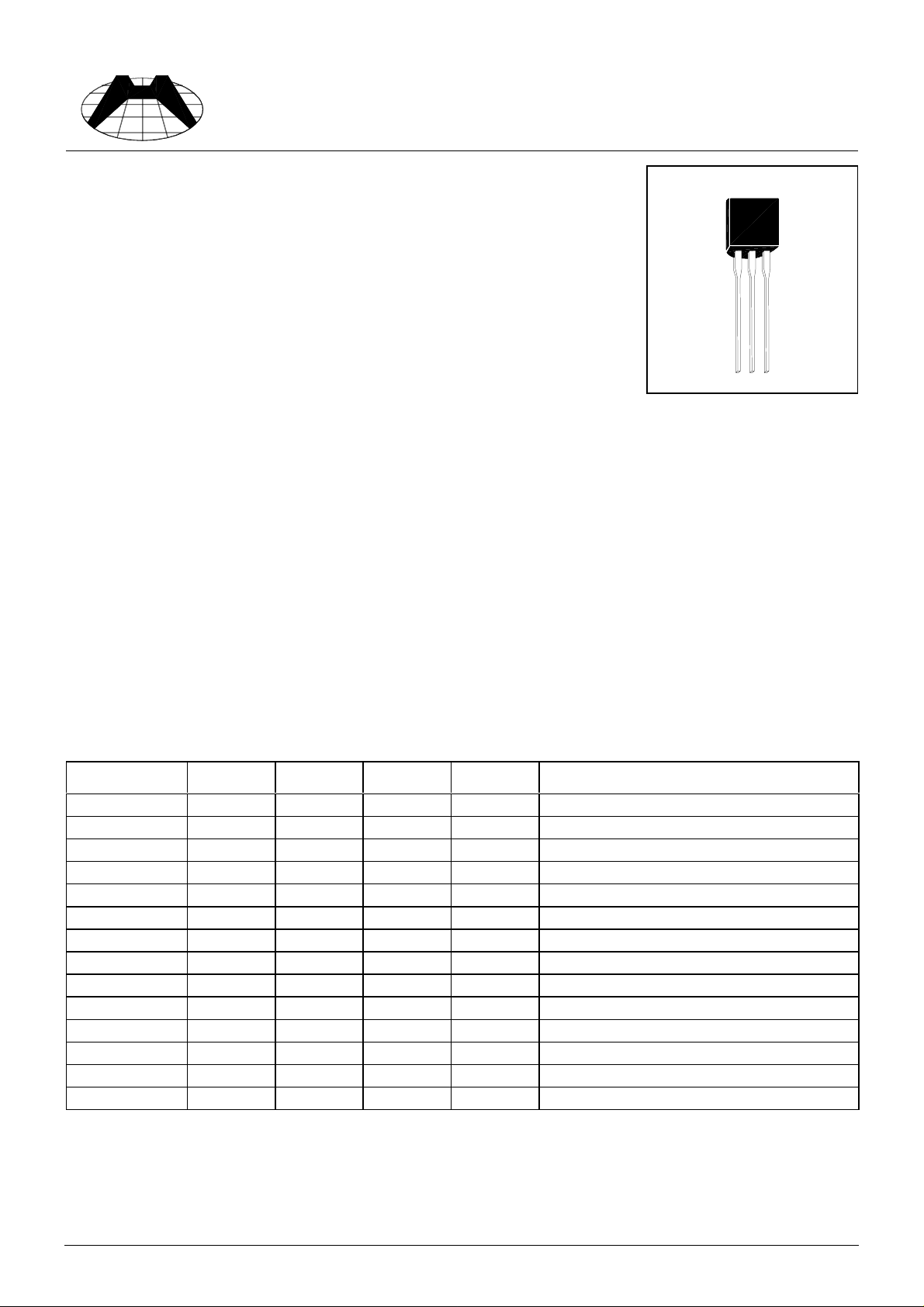
HMPS8599
PNP SILICON TRANSISTOR
Description
HMPS8599 is designed for general purpose amplifier applications.
Features
Low Collector-Emitter Saturation Voltage
•
HMPS8599 is complementary to HMPS8099
•
Absolute Maximum Ratings
Maximum Temperatures
•
Storage Temperature............................................................................................ -55 ~ +125 °C
Junction Temperature................................................................................... +150 °C Maximum
Maximum Power Dissipation
•
Total Power Dissipation (Ta=25°C)............................................................................... 625 mW
Maximum Voltages and Currents (Ta=25°C)
•
VCBO Collector to Base Voltag e....................................................................................... -80 V
VCES Collector to Emitter Voltage..................................................................................... -80 V
VEBO Emitter to Base Voltage ............................................................................................ -5 V
IC Collector Current...................................................................................................... -500 mA
Characteristics
Symbol Min. Typ. Max. Unit Test Co nditions
BVCBO -80 - - V IC=-100uA, IE=0
BVCEO -80 - - V IC=-10mA, IB=0
BVEBO -5 - - V IE=-10uA, IC=0
ICBO - - -100 nA VCB=-80V, IE=0
IEBO - - -100 nA VEB=-4V, IC=0
ICEO - - -100 nA VCE=-60V, IB=0
*hFE1 100 - 300 IC=-1mA, VCE=-5V
*hFE2 100 - - IC=-10mA, VCE=-5V
*hFE3 75 - - IC=-100mA, VCE=-5V
*VCE(sat)1 - - -0.4 V IC=-100mA, IB=-5mA
*VCE(sat)2 - - -0.3 V IC=-100mA, IB=-10mA
VBE(on) -0.6 - -0.8 V IC=-10mA, VCE= -5V
fT 150 - - MHz VCE=-5V, IC=-10mA, f=100MHz
Cob - - 8 PF VCB=-5V, IE=0, f=1MHz
(Ta=25°C)
*Pulse Test : Pulse Width ≤380us, Duty Cycle≤2%
HSMC Product Specification
Page 2
HI-SINCERITY
MICROELECTRONICS CORP.
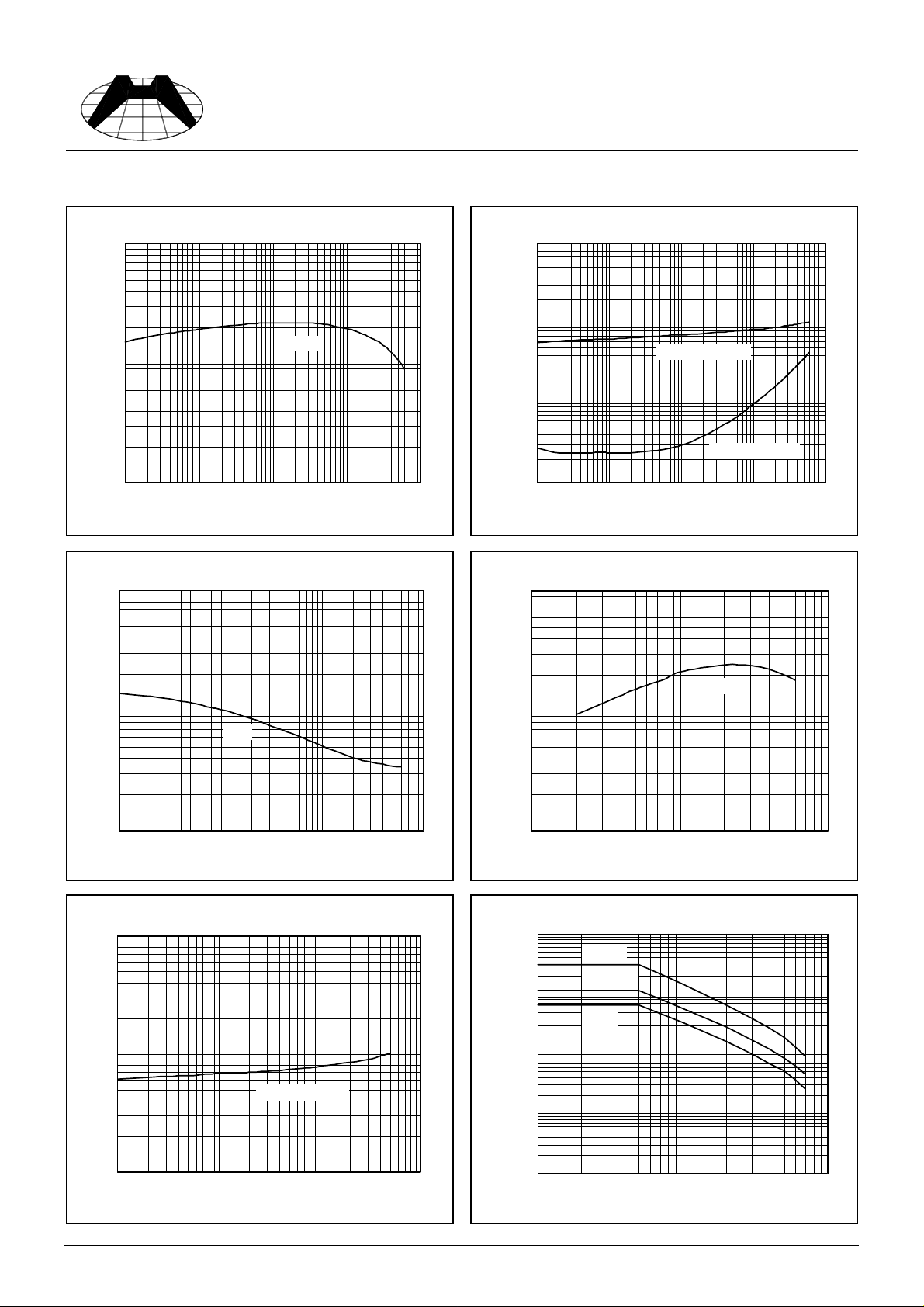
Characteristics Curve
Spec. No. : HE6319-B
Issued Date : 1996.07.18
Revised Date : 2000.10.01
Page No. : 2/4
1000
Current Gain & Collector Current
VCE=5V
100
hFE
10
0.1 1 10 100 1000
100
Capa citance & Rev er se-Bia sed Vol t age
Collector Curren t ( mA)
10000
1000
BE(sat)
V
100
Satu r ation Vol tage (m V)
10
0.1 1 10 100 1000
Collector Curren t ( mA)
@ IC=10I
CE(sat)
V
B
@ IC=10I
Cut o ff Fr equency & Col lector Current
1000
Saturation Voltage & Collector Current
B
10
Cob
Capac itance (pF)
1
0.1 1 10 100
Reverse Biased Vol t age ( V)
On Volta ge C ollector Current
10
1
On Voltage (V)
BE(ON)
V
@ VCE=5V
VCE=20V
100
Cutoff Frequency (MHz)
10
1 10 100
Collector Curren t ( mA)
Safe Operating Area
10000
PT=1ms
PT=100ms
PT=1s
(mA)
C
Collector Curren t- I
1000
100
10
0.1
1 10 100 1000
Collector Curren t ( mA)
1
1 10 100
Forwar d Biased Vol tage-VCE (V)
HSMC Product Specification
Page 3

HI-SINCERITY
MICROELECTRONICS CORP.
Spec. No. : HE6319-B
Issued Date : 1996.07.18
Revised Date : 2000.10.01
Page No. : 3/4
700
600
500
400
300
200
Power Dissipation-PD(mW)
100
0
0 20 40 60 80 100 120 140 160
Ambient Tem p er at ure- Ta(oC)
PD-Ta
HSMC Product Specification
Page 4

HI-SINCERITY
g
MICROELECTRONICS CORP.
TO-92 Dimension
A
Spec. No. : HE6319-B
Issued Date : 1996.07.18
Revised Date : 2000.10.01
Page No. : 4/4
α
2
Marking :
C
B
31
2
α
3
HSMC Logo
Part Number
Date Code
HSMC Logo
D
Part Number
H
α
I
1
G
Style : Pin 1.Emitter 2.Base 3.Collec tor
Product Series
Rank
Laser Mark
Product Series
Ink Mark
E
DIM
F
Inches Millimeters Inches Millimeters
Min. Max. Min. Max.
3-Lead TO-92 Plastic Package
HSMC Packa
e Code : A
DIM
Min. Max. Min. Max.
A 0.1704 0.1902 4.33 4.83 G 0.0142 0.0220 0.36 0.56
B 0.1704 0.1902 4.33 4.83 H - *0.1000 - *2.54
C 0.5000 - 12.70 - I - *0.0500 - *1.27
D 0.0142 0.0220 0.36 0.56
E - *0.0500 - *1.27
F 0.1323 0.1480 3.36 3.76
Notes :
Material :
• Lead : 42 Alloy ; solder plating
• Mold Compound : Epoxy resin family, flammability solid burning class:UL94V-0
1.Dimension and tolerance based on our Spec. dated Apr. 25,1996.
2.Controlling dimension : millimeters.
3.Maximum lead thickness includes lead finish thickness, and minimum lead thickness is the minimum thickness of base material.
4.If there is any question with packing specification or packing method, pleas e contact your l ocal HSMC sal es office.
1
α
2
α
3
α
-
-
-
*5
*2
*2
°
°
°
-
-
-
*:Typical
*5
°
*2
°
*2
°
Important Notice:
• All rights are reserved. Reproduction in whole or in part is prohibited without the prior written approval of HSMC.
• HSMC reserves the right to make changes to its products without notice.
•
HSMC semiconductor products are not warranted to be suitable for use in Life-Support Applications, or systems.
• HSMC assumes no liability for any consequence of customer product design, infringem ent of pat ents, or applic ati on assistance.
Head Office And Factory :
•
Head Office
Tel : 886-2-25212056 Fax : 886-2-25632712, 25368454
•
Factory 1 :
Tel : 886-3-5983621~5 Fax : 886-3-5982931
•
Factory 2 :
Tel : 886-3-5977061 Fax : 886-3-5979220
(Hi-Sincerity Microelectronics Corp.) : 10F.,No. 61, Sec. 2, Chung-Shan N. Rd. Taipei Taiwan R.O.C.
No. 38, Kuang Fu S. Rd., Fu-Kou Hsin-Chu Industrial Park Hsin-Chu Taiwan. R.O.C
No. 17-1, Ta-Tung Rd., Fu-Kou Hsin-Chu Industrial Park Hsin-Chu Taiwan. R.O.C
HSMC Product Specification
 Loading...