

Page 1
Silicon Bipolar RFIC
900 MHz Vector Modulator
Technical Data
HPMX-2003
Features
• 800–1000 MHz Output
Frequency Range
• +6 dBm Peak P
out
• Unbalanced 50 Ω Output
• Internal 90° Phase Shifter
• 5 Volt, 36 mA Bias
•
SO-16 Surface Mount Package
Applications
• Direct Modulator for 900
MHz Cellular Telephone
Handsets, Including GSM,
JDC, and NADC
• Direct Modulator for
900␣ MHz ISM Band SpreadSpectrum Transmitters and
LANs
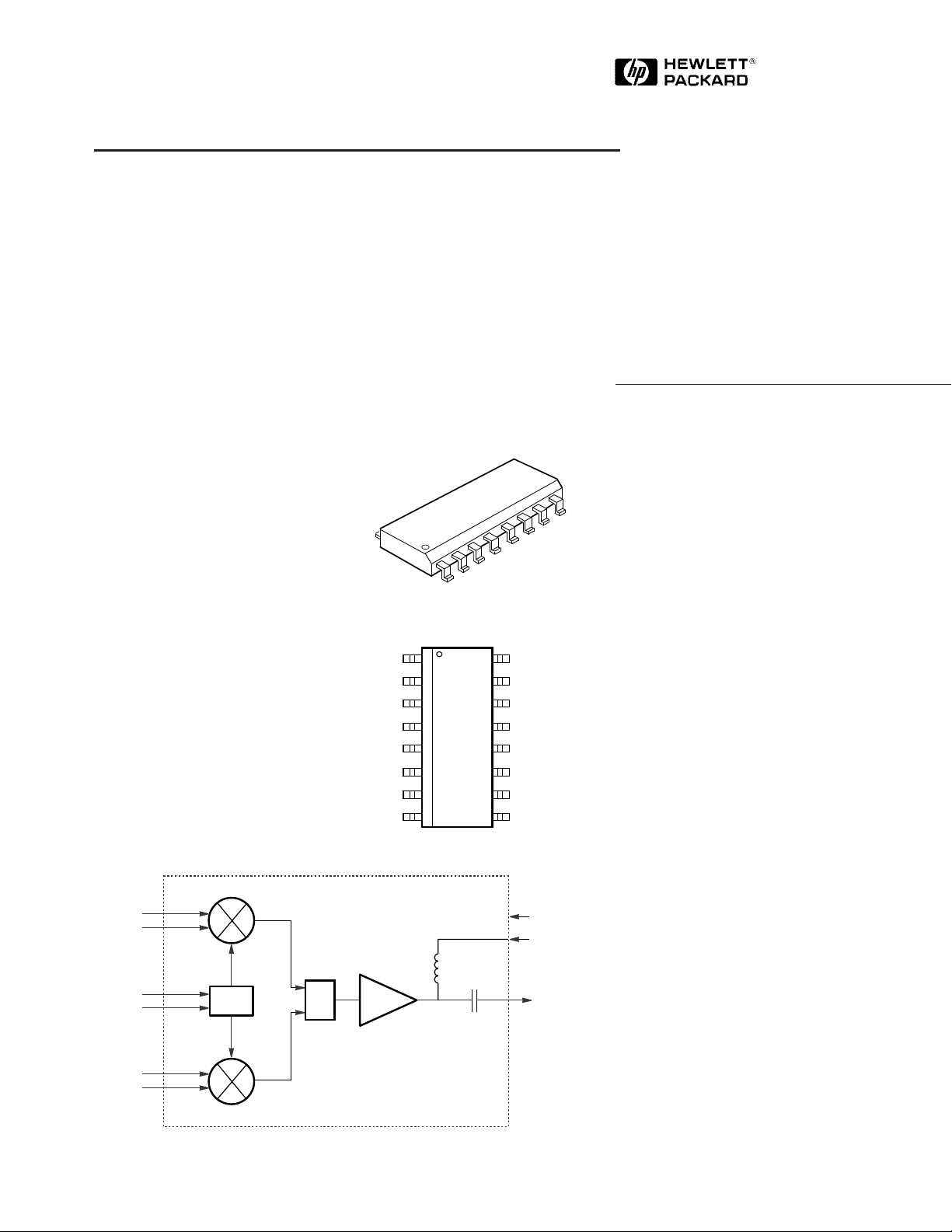
Functional Block Diagram
Plastic SO-16 Package
Pin Configuration
V
CC
V
CC
GROUND 3
GROUND 4
Q
ref
Q
mod
LO
in
LO
gnd
1
2
5
6
7
8
16 V
CC
15 RF
14 GROUND
13 GROUND
12 I
ref
11 I
mod
10 GROUND
9 DO NOT CONNECT
Description
Hewlett Packard’s HPMX-2003 is a
Silicon RFIC direct conversion
vector modulator designed for use
at output frequencies between
800␣ MHz and 1 GHz. Housed in a
SO-16 surface mount plastic package, the IC contains two matched
Gilbert cell mixers, an RC phase
shifter, a summer, and an output
amplifier complete with 50 Ω
L
out
impedance match and DC block.
This device is suitable for use in
direct and offset-loop modulated
portable and mobile telephone
handsets for cellular systems such
as GSM, North American Digital
Cellular and Japan Digital Cellular. It can also be used in digital
transmitters operating in the
900 MHz ISM (Industrial-Scientific-Medical) band, including use
in Local Area Networks (LANs).
I
mod
I
ref
LO +
LO –
Q
ref
Q
mod
5965-9103E
The HPMX-2003 is fabricated with
Hewlett-Packard’s 25 GHz
ISOSAT-II process, which
0°
I MIXER
V
CC
V
L
CC
combines stepper lithography,
PHASE
φ
SHIFTER
90°
Q MIXER
Σ
SUMMER
OUTPUT
AMPLIFIER
•
RF
out
50 Ω ZO
unbalanced
ion-implantation, self-alignment
techniques, and gold metallization
to produce RFICs with superior
performance, uniformity and
reliability.
7-38
Page 2
HPMX-2003 Absolute Maximum Ratings, T
= 25° C
A
Absolute
Symbol Parameter Units Maximum
P
diss
LO
in
V
CC
∆V
Imod
∆V
Qmod
V
, V
Iref
T
STG
T
j
Power Dissipation
LO Input Power dBm 15
Supply Voltage V 10
, Swing of V
or V
Reference Input Levels
Qref
Qmod
Imod
about V
Storage Temperature °C -65 to +150
Junction Temperature °C 150
[2,3]
about V
Qref
Iref
[4]
[4]
m W 500
V
p-p
V5
Thermal Resistance
[1]
Notes:
1. Operation of this device above any one
of these parameters may cause
permanent damage.
2. TC = 25°C (TC is defined to be the
[4]
5
[4]
temperature at the end of pin 3 where it
contacts the circuit board).
3. Derate at 8 mW/°C for TC > 88°C.
4. Do not exceed VCC by more than 0.8 V.
θjc =125°C/W
[2]
:
HPMX-2003 Guaranteed Electrical Specifications, T
VCC = 5 V, LO= -12 dBm at 900 MHz (Unbalanced Input), V
Iref
= V
= 25° C, ZO = 50 Ω
A
= 2.5 V (Unless Otherwise Noted).
Qref
Symbol Parameters and Test Conditions Units Min. Typ. Max.
LO
ε
P
I
d
out
leak
mod
Device Current mA 36 44
Output Power V
P
- LO at Output V
out
Average % 4 7
√
(V
- 2.5)2 + (V
Imod
= V
Imod
Qmod
Qmod
= V
Imod
Qmod
- 2.5)2= 1.25 V
= 3.75 V dBm +4.0 +6
= 2.5 V dBc +30 +37
Modulation
Error
HPMX-2003 Summary Characterization Information, T
VCC = 5 V, LO = -12 dBm at 900 MHz (Unbalanced Input), V
Iref
= V
Qref
= 25°C, ZO = 50 Ω
A
= 2.5 V (Unless Otherwise Noted).
Symbol Parameters and Test Conditions Units Typ.
R
in
R
in-gnd
VSWR
Input Resistance (I
mod
to I
ref
or Q
mod
to Q
) Ω 10 k
ref
Input Resistance to Ground (Any I, Q Pin to Ground) Ω 10 k
LO VSWR (50 Ω) GSM: 890-915 MHz Bandwidth 1.5:1
LO
NADC: 824-850 MHz Bandwidth 1.5:1
JDC: 940-960 MHz Bandwidth 1.5:1
VSWR
IM
A
i
P
i
Output VSWR (50 Ω) (Tuned by GSM: 890-915 MHz Bandwidth 1.2:1
O
Placement of V
Capacitor – NADC: 824-850 MHz Bandwidth 1.1:1
ccL
See Figures 22, 32, and 42) JDC: 940-960 MHz Bandwidth 1.2:1
Output Noise Floor
V
= V
Imod
DSB Third Order Intermodulation Products dBc +34
3
= 3.75 V dBm/Hz -134
Qmod
RMS Amplitude Error dB 0.3
RMS Phase Error degrees 2
7-39
Page 3
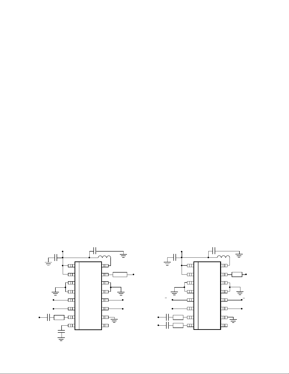
HPMX-2003 Pin Description
VCC (pins 1,2)
These two pins provide DC power
to the mixers in the RFIC, and are
connected together internal to the
package. They should be connected to a 5 V supply, with appropriate AC bypassing (1000 pF typ.)
used near the pins, as shown in
figures 1 and 2. The voltage on
these pins should always be
kept at least 0.8 V more posi-
tive than the DC level on any
of pins 5, 6, 11, or 12. Failure to
do so may result in the modulator
drawing sufficient current
through the data or reference
inputs to damage the IC.
Ground (pins 3, 4, 10, 13 & 14)
These pins should connect with
minimal inductance to a solid
ground plane (usually the backside of the PC board). Recommended assembly employs
multiple plated through via holes
where these leads contact the PC
board.
I
(pin 12) and Q
ref
I␣ (pin 11) and Q (pin 6) Inputs
The I and Q inputs are designed
for unbalanced operation but can
be driven differentially with simi-
(pin 5),
ref
lar performance. The recommended level of unbalanced I and
Q signals is 2.5 V
with an aver-
p-p
age level of 2.5 V above ground.
The reference pins should be DC
biased to this average data signal
level (VCC/2 or 2.5 V typ.). For
single ended drive, pins 5 and 12
can be tied together. For balanced
operation, 2.5 V
applied across the I
Q
mod/Qref
pairs. The average level
signals may be
p-p
mod/Iref
and the
of all four signals should be about
2.5 V above ground. The impedance between any I or Q and
ground is typically 10 K Ω and the
impedance between I
Q
mod
and Q
is typically 10 KΩ.
ref
mod
and I
ref
or
The input bandwidth typically
exceeds 40 MHz. It is possible to
reduce LO leakage through the IC
by applying slight DC imbalances
between I
and Q
and I
mod
(see section entitled
ref
and/or Q
ref
mod
“HPMX-2003 Using Offsets to Improve Lo Leakage”). All performance data shown on this data
sheet was taken with unbalanced
I/Q inputs.
LO Input (pins 7 and 8)
The LO input of the HPMX-2003 is
balanced and matched to 50 For
drive from an unbalanced LO, pin
7 should be AC coupled to the LO
using a 50 Ω transmission line and
a blocking capacitor (1000 pF
typ.), and pin 8 should be AC
grounded (1000 pF capacitor
typ.), as shown in figure 1. For
drive from a balanced LO source,
50 Ω transmission lines and blocking capacitors (1000 pF typ.) are
used on both pins 7 and 8, as
shown in figure 2. The internal
phase shifter allows operation
from 800 - 1000 MHz. The recommended LO input level is -12 dBm.
All performance data shown on
this data sheet was taken with unbalanced LO operation.
RF Output (pin15)
The RF output of the HPMX-2003
is configured for unbalanced
operation. The output is internally
DC blocked and matched to 50 Ω,
so a simple 50 Ω microstrip line is
all that is required to connect the
modulator to other circuits.
V
(pin 16)
CCL
Pin 16 is the VCC input for the output stage of the IC. It is not internally connected to the other V
CC
pins. The external connection allows the addition of a small inductor (0 - 6 nH) to tune the output
for minimum VSWR, depending
upon the operating frequency.
+5 V
1000 pF
Q
ref
Q
mod
LO
in
1000 pF
1000 pF
Figure 1. HPMX-2003 Connections Showing Unbalanced LO
and I, Q Inputs.
1000 pF
1
2
3
4
5
6
7
8
16
15
14
13
12
11
10
OPTIONAL INDUCTOR
9
DO NOT CONNECT
I
I
RF
ref
mod
out
7-40
1000 pF
Q
mod I
1000 pF
LO
+
in
LO
–
in
1000 pF
Figure 2. HPMX-2003 Connections Showing Balanced LO
and I, Q Inputs.
+5 V
Q
ref
1000 pF
1
2
3
4
5
6
7
8
16
15
14
13
12
11
10
9
OPTIONAL INDUCTOR
DO NOT CONNECT
I
ref
mod
RF
out
Page 4
HPMX-2003 Typical Data Measurement
Direct measurement of the amplitude and phase error at the output
is an accurate way to evaluate
modulator performance. By measuring the error directly, all the
harmonics, LO leakage, etc. that
show up in the output signal are
accounted for. Figure 3, below,
shows the test setup that was used
to create the amplitude and phase
error plots (figures 12 and 13).
Amplitude and phase error are
measured by using the four channel power supply to simulate I and
Q input signals. Real 2.5 V
Q signals would swing 1.25 volts
above and below an average 2.5 V
level, therefore, a “high” level input is simulated by applying
3.75␣ V, and a “low” level by applying 1.25 V to the I and/or Q inputs.
p-p
I and
Amplitude and phase are
measured by setting the network
analyzer for an S21 measurement
at frequency of choice. Set the
port 1 stimulus level to the LO
level you intend to use in your circuit (-12 dBm for the data sheet).
A 6-10 dB attenuator can be
placed in the line to port 2 to prevent network analyzer overload,
depending upon the network analyzer you are using.
By adjusting the V
Imod
and V
Qmod
settings you can step around the
I, Q vector circle, reading magnitude and phase at each point.
The relative values of phase and
amplitude at the various points
will indicate the accuracy of the
modulator. Note: you must use
very low ripple power supplies
for the reference, V
Imod
, and V
Qmod
supplies. Ripple or noise of only a
few millivolts will appear as wob-
bling phase readings on the network analyzer.
The same test setup shown below
is used to measure input and output VSWR, reverse isolation, and
power vs. frequency. V
V
are set to 3.75 V and the
Qmod
Imod
and
appropriate frequency ranges are
swept. S11 provides input VSWR
data, S22 provides output VSWR
data. S21 provides power output
(add source power to S21 derived
gain).
LO leakage data shown in figures
18, and 19 is generated by setting
V
Imod
= V
Qmod
= V
Iref
= V
Qref
= 2.5 V
then performing an S21 sweep.
Since phase is not important for
these measurements, a scalar network analyzer or a signal generator and spectrum analyzer could
be used.
HP-8753C VECTOR NETWORK ANALYZER
PORT 1
Q
5 V
HP-6626A
SYSTEM DC POWER SUPPLY
(FOUR OUTPUTS)
2.5 V
Figure 3. Test Setup for Measuring Amplitude and Phase Error, Input and Output
VSWR, Power Output and LO Leakage of the Modulator.
V
Qmod
V
Imod
VER 1
H
HPMX-2003/5
I
R
C
LO
C
C
C
OUT
PORT 2
R
V
CC
5 V
7-41
Page 5
HPMX-2003 Typical Performance
45
42
39
36
DEVICE CURRENT (mA)
33
30
-55
-35 -15
5
25 45 65 85
TEMPERATURE (°C)
Figure 4. HPMX-2003 Device Current
vs. Temperature, V
10
8
6
4
OUTPUT POWER (dBm)
2
0
-55
-35 -15
= 5 V.
CC
5
25 45 65 85
TEMPERATURE (°C)
Figure 6. HPMX-2003 Power Output
vs. Temperature at 900 MHz,
LO␣ =␣ -12␣ dBm, V
V
= V
Iref
= 2.5 V, V
Qref
Imod
= V
CC
Qmod
= 5 V.
= 3.75 V,
50
45
40
35
DEVICE CURRENT (mA)
30
25
4.5
4
V
CC
5
(VOLTS)
5.5 6
Figure 5. HPMX-2003 Device Current
vs. VCC, T
OUTPUT POWER (dBm)
= 25° C.
A
10
8
6
4
2
0
-2
-4
-6
-8
-10
4.5
4.25 4.75 5.25 5.75
4
V
CC
5
(VOLTS)
4.25 V
3.75 V
3.25 V
3.0 V
2.75 V
5.5 6
Figure 7. HPMX-2003 Power Output
vs. V
and I, Q Level at 900 MHz,
CC
LO␣ =␣ -12 dBm, V
Imod
= V
Qmod
, T
A
= 25° C.
10
8
6
4
OUTPUT POWER (dBm)
2
0
-25
-20
-15 -10 -5 0
LO INPUT POWER (dBm)
Figure 8. HPMX-2003 Power Output
vs. LO Level at 900 MHz, VCC = 5 V,
V
= V
Imod
Qmod
= 3.75 V , T
= 25° C.
A
5:1
4:1
3:1
INPUT VSWR
2:1
1:1
750
-55 °C
85 °C
850
FREQUENCY (MHz)
950 1050
Figure 9. HPMX-2003 LO Input VSWR
vs. Frequency and Temperature,
V
=␣ 5 V.
CC␣
5:1
4:1
3:1
OUTPUT VSWR
2:1
-55 °C
1:1
750
850
85 °C
950 1050
FREQUENCY (MHz)
Figure 10. HPMX-2003 Output VSWR
vs. Frequency and Temperature.
7-42
2:1
1.8:1
1.6:1
1.4:1
OUTPUT VSWR
1.2:1
1:1
4
4.5
V
CC
5
(VOLTS)
5.5 6
Figure 11. HPMX-2003 Output VSWR
vs. V
at 900 MHz, T
CC
= 25° C.
A
Page 6

HPMX-2003 Modulation Accuracy (Sample Part)
1
0.5
0
-0.5
OUTPUT AMPLITUDE ERROR (dB)
-1
0
90
85 °C
-55 °C
INPUT PHASE (DEGREES)
180
270 360
Figure 12. HPMX-2003 Amplitude Error vs. Input Phase at 900 MHz,
V
= 5 V, √(V
CC␣
-2.5)2 + (V
Imod
- 2.5)2 = 1.25 V, LO = -12 dBm.
Qmod
25° C␣ Curve Deleted for Clarit y.
4
2
0
-2
OUTPUT PHASE ERROR (DEGREES)
-4
0
-55 °C
85 °C
90
INPUT PHASE (DEGREES)
180
270 360
Figure 13. HPMX-2003 Output Phase Error vs. Input Phase at 900 MHz,
V
= 5 V, √(V
CC␣
25° C Curve Deleted for Clarity.
8
6
4
2
OUTPUT MODULATION ERROR (%)
0
0
Figure 14. Modulation Error vs. Input Phase at 900 MHz, V
√(V
-2.5)2 + (V
Imod
-2.5)2 + (V
Imod
Qmod
-2.5)2 = 1.25 V, LO = -12 dBm.
Qmod
85 °C
-55 °C
90
INPUT PHASE (DEGREES)
-2.5)2 = 1.25 V, LO = -12 dBm. Percent Modulation
180
270 360
= 5 V,
CC
Error is Calculated from the Values of Amplitude and Phase Error.
7-43
Page 7

HPMX-2003 Single and
OUTPUT POWER (dB )
Double Sideband
and DSB output spectrum graphs
(figures 15 and 16).
flect the performance of the
modulator IC.
Performance
Single sideband (SSB) and double
sideband (DSB) tests are sometimes used to evaluate modulator
performance. Figure 17, below,
shows the test equipment setup
that was used to create the SSB
The phase shift provided by the I
and Q signal generators must be
very close to 90 degrees and the
amplitude of the two signals must
be matched within a few millivolts
or results will not accurately re-
The I, Q signal generator must put
out low distortion signals or the
output spectrum will show high
harmonic levels that reflect the
performance of the signal generator, not the modulator.
HPMX-2003 Typical Sideband Performance Data
SSB: V
DSB: V
= V
Iref
Iref
= V
= 2.5 V, V
Qref
= 2.5 V, V
Qref
Imod
Imod
= V
+1.25 sin (2π f t), V
Iref
= V
+1.25 cos (2π f t), V
Iref
Qmod
Qmod
= V
= V
+ 1.25 cos (2π f t), f = 25 kHz
Qref
+ 1.25 cos (2π f t), f = 25 kHz
Qref
Symbol Parameters and Test Conditions Units SSB DSB
P
LSB
LO
leak
P
USB
IM
3
5
-5
-15
-25
-35
-45
-55
OUTPUT POWER (dBm)
-65
-75
899.9
899.95
Lower Sideband Power Output dBm +30
LO Suppression dBc 34 31
Upper Sideband Power Output dBm -32 0
Third Order Intermodulation Products dBm NA -34
900 900.05 900.1
FREQUENCY (MHz)
Figure 15. Single Sideband Output Spectrum.
LO␣ =␣ -12␣ dBm at 900 MHz. The Test Setup is Shown
in␣ Figure␣ 1 7.
HP-8657B SYNTHESIZED SIGNAL GENERATOR
5
-5
-15
-25
-35
-45
OUTPUT POWER (dBm)
-55
-65
-75
899.9
899.95
900 900.05 900.1
FREQUENCY (MHz)
Figure 16. Double Sideband Output Spectrum.
LO␣ =␣ -12␣ dBm at 900 MHz. The Test Setup is Shown
in␣ Figure 1 7.
COS
HP-3245A UNIVERSAL SOURCE
OPT 001
DUAL OUTPUTS WITH 90 DEGREE
RELATIVE PHASE SHIFT
DSB
SIN
SSB
Figure 17. HPMX-2003 Single/Double Sideband Test Setup.
VER 1
H
HPMX-2003/5
I
R
HP-8595A SPECTRUM ANALYZER
LO
C
C
C
OUT
V
CC
5 V
C
HP-6626A
SYSTEM DC
POWER SUPPLY
R
Q
7-44
Page 8

HPMX-2003 Using Offsets to Improve LO Leakage
It is possible to improve on the
excellent performance of the
HPMX-2003 for applications that
are particularly sensitive to LO
leakage. The nature of the
improvement is best understood
by examining figures 18 and 19,
below.
LO leakage results when normal
variations in the wafer fabrication
process cause small shifts in the
values of the modulator IC’s internal components. These random
variations create an effect equivalent to slight DC imbalances at the
input of each (I and Q) mixer. The
DC imbalances at the mixer inputs are multiplied by ± 1 at the
LO frequency and show up at the
output of the IC as LO leakage.
It is possible to externally apply
small DC signals to the I and Q inputs and exactly cancel the internally generated DC offsets. This
will result in sharply decreased
LO leakage at precisely the frequency and temperature where
the offsets were applied (see figure 18).
This improvement is not very useful if it doesn’t hold up over frequency and temperature changes.
The lower curve in figure 18
shows how the offset-adjusted LO
leakage varies versus frequency.
Note that it remains below
-45␣ dBm over most of the frequency range shown. In the
20␣ MHz range centered at
900␣ MHz, the level is closer to
-55␣ dBm.
Figure 19 shows the performance
of the offset adjusted LO leakage
over temperature. Note that the
adjusted curve is at a level below
-50 dBm over most of the temperature range.
The net result of using
externally applied offsets with
the HPMX-2003 is that an LO
leakage level below -40 dBm
can typically be achieved over
both frequency and
temperature.
The magnitude of the required external offset varies randomly from
part to part and between the I and
Q mixers on any given IC. Offsets
can range from -56 mV to +56 mV.
External offsets may be applied
either by varying the average level
of the I and Q modulating signals,
or by varying the voltages at the
I
and Q
ref
pins of the modulator.
ref
-20
-35
-50
OUTPUT POWER (dBm)
-65
-80
-55
-35 -15
Figure 18. LO Leakage vs. Frequency
Without DC Offsets (Upper Curve)
and LO Leakage vs. Frequency With
DC Offsets (Adjusted for Minimum LO
Leakage at 900 MHz). T
5 V, V
= V
Iref
5
25 45 65 85
TEMPERATURE (°C)
= 25° C, V
= 2.5 V, LO = -12 dBm.
Qref
A
CC
=
-20
-30
-40
-50
OUTPUT POWER (dBm)
-60
Figure 19. LO Leakage With No DC
Offsets vs. Temperature (Upper
Curve) and LO Leakage With DC
Offsets (Adjusted for Minimum
Leakage at 25°C) vs. Temperature
(Lower Curve). Frequency = 900 MHz,
VCC = 5 V, V
LO␣ =␣ -12␣ dBm.
750
FREQUENCY (MHz)
= V
Iref
Qref
850
= 2.5 V,
950 1050650 1150
7-45
Page 9

HPMX-2003 Modulation Spectrum Diagrams
Figure 20, below, shows the test
setup that was used to generate
the modulation spectrum diagrams that appear on the GSM,
JDC and NADC applications pages
of this data sheet. The major differences between the tests are
summarized in the table below.
The modulation spectra are created by setting the function generator to the appropriate bit-clock
frequency. The pattern generator
is set to produce a pseudorandom
serial bit stream (n␣ = 20) that is
NRZ coded. The pseudorandom
bit stream which simulates the
serial data in a digital phone is fed
to the base-band processor that
stream (I and Q) and then filters
each according to the requirements of the digital telephone system being simulated. The I and Q
signals from the baseband filter
are then DC offset by 2.5 V using
the op-amp circuit. The output of
the modulator is monitored using
a spectrum analyzer.
splits it into a two bit parallel
System Bit Clock Frequency Baseband Filter Channel (LO) Frequency
GSM 270 kHz 0.3 GMSK (HP 8657B) 900 MHz
JDC 42 kHz α = 0.5 π/4 DQPSK (HP 8657D) 950 MHz
NADC 48.6 kHz α = 0.35 π/4 DQPSK (HP 8657D) 835 MHz
HP-8563E
SPECTRUM ANALYZER
HP-3314A
FUNCTION
GENERATOR
HP-3780A
PRBS GENERATOR
DATACLOCK
HP-8657B
OR
HP-8657D
BASEBAND
PROCESSOR
1
I
π/4DQPSK Q INPUT
ALL R = 5 k OP-AMP: TL-084 I CHANNEL IS IDENTICAL
I
Q
R
ref
+5 V
OP-AMP CIRCUIT
(SEE ABOVE)
C
HPMX-2003/5
OUT
C
H
C
C
5 V
•
•
VER 1
C
LO
Q
R
V
CC
–
+
I + 2.5 V TO 1
2.5 V TO I
Q + 2.5 V TO 2
2.5 V TO Q
SIGNAL GENERATOR
835-950 MHz
2
Q
ref
Q + 2.5 V
Qref = 2.5 V
ref
ref
HP-8657B
Figure 20. Test Equipment Setup for Modulation Spectrum Diagrams.
7-46
Page 10

HPMX-2003 GSM
Applications
The GSM System
GSM (Group Speciale Mobile)
commonly refers to the European
digital cellular telephone system
standard. Digital cellular phones
for the European market must
conform to this standard. The
GSM system is characterized by
200 kHz channel spacing and mobile to base transmit frequencies
of 890 - 915 MHz. The primary
modulation characteristics include 0.3 GMSK filtering of the I
and Q signals and 270 kbps transmission rate.
Critical Performance
Parameters
GSM standards require that the
telephone exhibit RMS phase error ≤ 5° and peak phase error <20° .
The modulated output spectrum
of the phone must lie within a
“spectral mask” which defines
maximum allowable radiation levels into adjacent and alternate
channels. Specifically, 200 kHz
from the channel center frequency
(f0), the output of the phone must
be at least 30 dB below the peak
output at f0. 400 kHz from f0 the
output must be 50-60 dB below
the peak output at f0 depending
upon the class of radio. Refer to
the GSM900 specifi-cations for
more detailed information.
HPMX-2003 Performance
Typical RMS phase error level of
2° and typical peak levels of 8°
makes the HPMX-2003 an excellent choice for GSM applications.
The output spectrum falls easily
within the GSM spectral mask,
and the high power and simple
output configuration mean lower
components count, reduced size
and higher system efficiency.
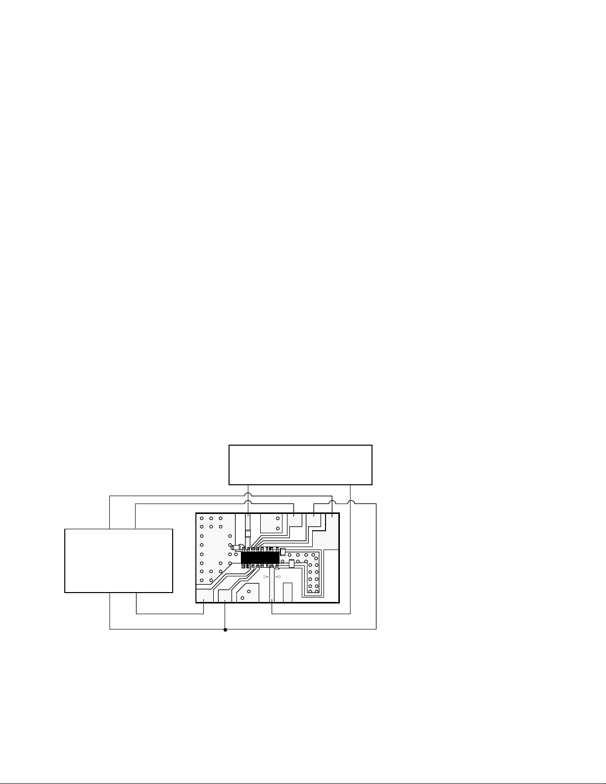
Particulars of Use
Many of the GSM application
performance graphs shown in this
data sheet were created using the
test board shown in figure 21,
below.
The only external components required by this IC are four chip
capacitors. One capacitor is used
as a DC block on the input transmission line. The second capacitor (at pin 8) provides an AC
ground to one side of the differential LO input. The third and fourth
capacitors (at pins 1 and 16) are
for VCC bypass.
The circuit board includes an inductive trace that can optionally
be used to minimize output VSWR
by placing a bypass capacitor at
various points along the inductive
line. Minimum VSWR for GSM
applications is achieved by placing the capacitor as shown in the
circle (inductance ≈2 nH).
The IC has an internal blocking
capacitor so the output is a simple
50 Ω transmission line. An
enlarged scale layout of the test
board can be found on the last
page of this data sheet.
VER. 1
C
C
H
HPMX-2003/5
I
Figure 21. HPMX-2003 GSM Test Board.
R
LO
C
OUT
Q
C
R
V
CC
5 V
7-47
Page 11

HPMX-2003 Typical Performance Data
0
RES BW = 3 kHz
VBW = 30 Hz
SWP = 60.0 SEC.
0
RES BW = 3 kHz
VBW = 30 Hz
SWP = 60.0 SEC.
GSM Applications
0
RES BW = 3 kHz
VBW = 30 Hz
SWP = 60.0 SEC.
-50
RF OUTPUT POWER (dBm)
-100
899
900 901
FREQUENCY (MHz)
Figure 22. HPMX-2003 GSM
Modulation Spectrum at -40°C.
2:1
1.75:1
890
900
FREQUENCY (MHz)
POWER >
< VSWR
910 920880 930
1.5:1
OUTPUT VSWR
1.25:1
1:1
Figure 25. HPMX-2003 Output VSWR
and Power vs. Frequency, V
LO␣ = -12 dBm, V
Unbalanced, V
T
=␣ 25 °C.
A␣
Iref
Imod
= V
= V
Qref
CC
= 3.75 V,
Qmod
= 2.5 V,
= 5 V,
-50
RF OUTPUT POWER (dBm)
-100
899
900 901
FREQUENCY (MHz)
Figure 23. HPMX-2003 GSM
Modulation Spectrum at 25°C.
8
7
6
5
OUTPUT POWER (dBm)
4
0
-10
-20
OUTPUT POWER (dBm)
-30
-40
850
875
25 °C
900
FREQUENCY (MHz)
Figure 26. HPMX-2003 LO Leakage vs.
Frequency and Temperature (Without
Offset Adjustment), VCC = 5 V,
LO␣ =␣ -12 dBm, V
V
= 2.5 V.
Qref
Imod
= V
-55 °C
85 °C
Qmod
925 950
= V
=
Iref
-50
RF OUTPUT POWER (dBm)
-100
899
900 901
FREQUENCY (MHz)
Figure 24. HPMX-2003 GSM
Modulation Spectrum at 85°C.
0
-20
900
85 °C
-55 °C
25 °C
925 950
-40
OUTPUT POWER (dBm)
-60
-80
850
875
FREQUENCY (MHz)
Figure 27. LO leakage vs. Frequency
and Temperature (With 25°C Offset
Adjustment), VCC = 5 V, LO = -12 dBm,
V
= V
Qref
= 2.5 V.
Iref
8
6
4
2
OUTPUT POWER (dBm)
0
-25
-15
-20
LO INPUT POWER (dBm)
-10 -5 0
Figure 28. HPMX-2003 Power Output
vs. LO Input Power at 900 MHz, VCC =
5␣ V, V
V
Iref
Imod
= V
= V
Qref
= 3.75 V, Unbalanced,
Qmod
= 2.5 V, T
= 25° C.
A
1
0.5
-0.5
OUTPUT AMPLITUDE ERROR (dB)
-1
85 °C
-55 °C
0
0
90
INPUT PHASE (DEGREES)
270 360180
Figure 29. HPMX-2003 Vector
Amplitude Error vs. Input Phase and
Temperature at 900 MHz, VCC = 5 V,
LO␣ = -12 dBm, V
Iref
= V
Qref
= 2.5 V.
Note: Modulation spectrum test conditions as follows: VCC = 5 V, LO = -12 dBm at 900 MHz, V
level = 2.5 V, V
Iref
= V
= 2.5 V, bit clock rate: 270 kHz, baseband filter: α = 0.3 GMSK.
Qref
7-48
4
2
0
-2
OUTPUT PHASE ERROR (DEGREES)
-4
0
-55 °C
85 °C
90
INPUT PHASE (DEGREES)
Figure 30. HPMX-2003 Vector Phase
Error vs. Input Phase and
Temperature at 900 MHz, VCC = 5 V,
LO = -12 dBm, Unbalanced, V
= 2.5 V.
= V
Imod
Qmod
= 2.5 V
, unbalanced, average
p-p
270 360180
= V
Iref
Qref
Page 12

HPMX-2003 NADC
Applications
The NADC System
NADC (North American Digital
Cellular) commonly refers to the
digital sections of the IS-55
cellular telephone system standard. Dual mode (FM/TDMA)
cellular phones for the North
American market must conform
to this standard. The NADC
system is characterized by 30 kHz
channel spacing and mobile to
base transmit frequencies of 824 849 MHz. The primary modulation
characteristics include π/4 DQPSK
filtering of the I and Q signals and
48.6 kbps transmission rate.
Critical Performance
Parameters
System specifications require that
the telephone exhibit RMS modulation error under 12% in the digital mode. The modulated output
spectrum of the phone must lie
within a “spectral mask” which
defines maximum allowable radiation levels into adjacent and alternate channels. Specifically, total
power radiated into the either adjacent channel must be at least
26␣ dB below the mean output
power. Total power radiated into
either alternate channel must be
at least 45 dB below the mean output power. Refer to the IS-55
specifications for more detailed
information.
HPMX-2003 Performance
The typical RMS modulation error
level of 4% makes the HPMX-2003
an excellent choice for NADC
applications. The output falls
easily within the NADC spectral
requirements, and the high power
and simple output configuration
mean lower components count,
reduced size and higher system
efficiency.
Particulars of Use
Many of the NADC application
performance graphs shown in this
data sheet were created using the
test board shown in figure 31,
below.
The only external components required by this IC are four chip
capacitors. One capacitor is used
as a DC block on the input transmission line. The second capacitor (at pin 8) provides an AC
ground to one side of the differential LO input. The third and fourth
capacitors (at pins 1 and 16) are
for VCC bypass.
The circuit board includes an inductive trace that can optionally
be used to minimize output VSWR
by placing a bypass capacitor at
various points along the inductive
line. Minimum VSWR for NADC
applications is achieved by placing the capacitor as shown in the
circle (inductance ≈ 6 nH).
The IC has an internal blocking
capacitor so the output is a simple
50 Ω transmission line. An enlarged scale layout of the test
board can be found on the last
page of this data sheet.
VER. 1
C
C
H
HPMX-2003/5
MR
I
Figure 31. HPMX-2003 NADC Test Board.
R
LO
Q
C
OUT
R
V
CC
5 V
C
7-49
Page 13

HPMX-2003 Typical Performance Data NADC Applications
0
-50
RF OUTPUT POWER (dBm)
-100
834.85
FREQUENCY (MHz)
RES BW = 3 kHz
VBW = 30 Hz
SWP = 9.00 SEC.
835.00 835.15
Figure 32. HPMX-2003 NADC
Modulation Spectrum at -40°C.
2:1
1.75:1
POWER >
1.5:1
OUTPUT VSWR
1.25:1
< VSWR
1:1
830
FREQUENCY (MHz)
845
Figure 35. HPMX-2003 Output VSWR
and Power vs. Frequency, VCC = 5 V,
LO␣ = -12 dBm, V
Unbalanced, V
T
=␣ 25 °C.
A␣
10
8
6
4
OUTPUT POWER (dBm)
2
0
-25
-20
= V
Imod
= V
Iref
-15
LO INPUT POWER (dBm)
= 3.75 V,
Qmod
= 2.5 V,
Qref
-10 -5 0
Figure 38. HPMX-2003 Power Output
vs. LO Input Power at 900 MHz, VCC =
5 V, LO = -12 dBm, V
V, Unbalanced, V
Iref
Imod
= V
Qref
= V
Qmod
= 2.5 V, TA =
= 3.75
8
7
6
5
4
860815
0
-50
RF OUTPUT POWER (dBm)
-100
834.85
FREQUENCY (MHz)
RES BW = 3 kHz
VBW = 30 Hz
SWP = 9.00 SEC.
835.00 835.15
Figure 33. HPMX-2003 NADC
Modulation Spectrum at 25°C.
0
-10
-20
OUTPUT POWER (dBm)
OUTPUT POWER (dBm)
-30
-40
810
820
-55 °C
25 °C
85 °C
840
830
FREQUENCY (MHz)
850 860
Figure 36. HPMX-2003 LO Leakage vs.
Frequency and Temperature (Without
Offset Adjustment), VCC = 5 V, LO
=␣ -12␣ dBm, V
Imod
= V
Qmod
= V
Iref
= V
Qref
2.5 V.
0.5
0.25
0
-0.25
OUTPUT AMPLITUDE ERROR (dB)
-0.5
0
-55 °C
85 °C
90
INPUT PHASE (DEGREES)
270 360180
Figure 39. HPMX-2003 Vector
Amplitude Error vs. Input Phase and
Temperature at 900 MHz, VCC = 5 V, LO
= -12 dBm, V
Iref
= V
Qref
= 2.5 V.
=
25°C.
Note: Modulation spectrum test conditions as follows: LO = -12 dBm at 835 MHz, VI = VQ = 2.5 V
= V
= 2.5 V, bit clock rate: 48.6 kHz, baseband filter: α = 0.35, π/4 DQPSK, VCC = 5 V.
Qref
0
-50
RF OUTPUT POWER (dBm)
-100
834.85
FREQUENCY (MHz)
RES BW = 3 kHz
VBW = 30 Hz
SWP = 9.00 SEC.
835.00 835.15
Figure 34. HPMX-2003 NADC
Modulation Spectrum at 85°C.
0
-20
-40
OUTPUT POWER (dBm)
-60
-80
810
85 °C
-55 °C
+25 °C
830
820
FREQUENCY (MHz)
840
850 860
Figure 37. LO Leakage vs. Frequency
and Temperature (With 25°C Offset
Adjustment), VCC = 5 V, LO = -12 dBm,
V
= V
2.5
-2.5
= 2.5 V.
Qref
5
85 °C
0
-5
0
90
INPUT PHASE (DEGREES)
-55 °C
270 360180
Iref
OUTPUT PHASE ERROR (DEGREES)
Figure 40. HPMX-2003 Vector Phase
Error vs. Input Phase and
Temperature at 900 MHz, VCC = 5 V, LO
= -12 dBm, Unbalanced, V
Iref
= V
Qref
=
2.5 V.
, unbalanced, average level = 2.5 V, V
p-p
Iref
7-50
Page 14

HPMX-2003 JDC
Applications
The JDC System
JDC (Japan Digital Cellular) commonly refers to the Japanese digital cellular telephone system
standard. Digital cellular phones
for the Japanese market must
conform to this standard. The JDC
system is characterized by 25 kHz
channel spacing and mobile to
base transmit frequencies of 940 –
960 MHz. The primary modulation
characteristics include π/4 DQPSK
filtering of the I and Q signals and
42 kbps transmission rate.
Critical Performance
Parameters
JDC standards require that the
telephone exhibit RMS modulation error ≤ 12.5%. The modulated
output spectrum of the phone
must lie within a “spectral mask”
which defines maximum allowable radiation levels into adjacent
and alternate channels. Specifi-
cally, 50 kHz from the channel
center frequency (f0), the output
of the phone must be at least
45␣ dB below the peak output at f0.
100 kHz from f0, the output must
be at least 60 dB below the peak
output at f0. Refer to the JDC
specifications for more detailed
information.
HPMX-2003 Performance
The typical RMS modulation error
level of 4% makes the HPMX-2003
an excellent choice for JDC applications. The output spectrum falls
easily within the JDC spectral
mask, and the high power and
simple output configuration mean
lower components count, reduced
size and higher system efficiency.
Particulars of Use
Many of the JDC application performance graphs shown in this
data sheet were created using the
test board shown in figure 41,below.
The only external components
required by this IC are four chip
capacitors. One capacitor is used
as a DC block on the input transmission line. The second capacitor (at pin 8) provides an AC
ground to one side of the differential LO input. The third and fourth
capacitors (at pins 1 and 16) are
for VCC bypass.
The circuit board includes an inductive trace that can optionally
be used to minimize output VSWR
by placing a bypass capacitor at
various points along the inductive
line. Minimum VSWR for JDC
applications is achieved by placing the capacitor as shown in the
circle (inductance ≈ 0 nH).
The IC has an internal blocking
capacitor so the output is a simple
50 Ω transmission line. An enlarged scale layout of this board
can be found on the last page of
this data sheet.
VER. 1
C
C
H
HPMX-2003/5
I
Figure 41. HPMX-2003 JDC Test Board.
R
LO
C
C
OUT
Q
R
V
CC
5 V
7-51
Page 15

HPMX-2003 Typical Performance Data
0
RES BW = 3 kHz
VBW = 30 Hz
SWP = 7.50 SEC.
0
RES BW = 3 kHz
VBW = 30 Hz
SWP = 7.50 SEC.
JDC Applications
0
RES BW = 3 kHz
VBW = 30 Hz
SWP = 7.50 SEC.
-50
RF OUTPUT POWER (dBm)
-100
949.875
950.00 950.125
FREQUENCY (MHz)
Figure 42. HPMX-2003 JDC
Modulation Spectrum at -40°C.
2:1
1.75:1
1.5:1
OUTPUT VSWR
1.25:1
1:1
POWER >
< VSWR
940
FREQUENCY (MHz)
960
Figure 45. HPMX-2003 Output VSWR
and Power vs. Frequency, VCC = 5 V,
LO␣ = -12 dBm, V
Unbalanced, V
T
=␣ 25 °C.
A␣
8
Iref
Imod
= V
= V
Qref
= 3.75 V,
Qmod
= 2.5 V,
-50
RF OUTPUT POWER (dBm)
-100
949.875
Figure 43. HPMX-2003 JDC
Modulation Spectrum at 25°C.
8
7
6
5
OUTPUT POWER (dBm)
4
980920
0
-10
-20
OUTPUT POWER (dBm)
-30
-40
920
Figure 46. HPMX-2003 LO Leakage vs.
Frequency and Temperature (Without
Offset Adjustment), VCC = 5 V,
LO␣ =␣ -12 dBm, V
V
= 2.5 V.
Qref
1
950.00 950.125
FREQUENCY (MHz)
-55 °C
85 °C
= V
960 980
= V
Qmod
940
FREQUENCY (MHz)
Imod
Iref
25 °C
=
-50
RF OUTPUT POWER (dBm)
-100
949.875
950.00 950.125
FREQUENCY (MHz)
Figure 44. HPMX-2003 JDC
Modulation Spectrum at 85°C.
0
-10
-20
OUTPUT POWER (dBm)
-30
-40
920
-55 °C
85 °C
940
FREQUENCY (MHz)
960 980
25 °C
Figure 47. LO Leakage vs. Frequency
and Temperature (With 25°C Offset
Adjustment), VCC = 5 V, LO = -12 dBm,
V
= V
Iref
= 2.5 V.
Qref
6
85 °C
6
4
2
OUTPUT POWER (dBm)
0
-25
-15
-20
LO INPUT POWER (dBm)
-10 -5 0
Figure 48. HPMX-2003 Power Output
vs. LO Input Power at 950 MHz, VCC =
5 V, V
V
Iref
Imod
= V
= V
= 2.5 V, T
Qref
= 3.75 V, Unbalanced,
Qmod
= 25° C.
A
0.5
85 °C
0
-0.5
OUTPUT AMPLITUDE ERROR (dB)
-1
0
90
INPUT PHASE (DEGREES)
-55 °C
Figure 49. HPMX-2003 Vector
Amplitude Error vs. Input Phase and
Temperature at 950 MHz, VCC = 5 V, LO
= -12 dBm, Unbalanced, V
2.5 V.
Iref
= V
Note: Modulation spectrum test conditions as follows: LO = -12 dBm at 950 MHz, V
V, V
= V
Iref
= 2.5 V, bit clock rate: 42 kHz, baseband filter: α = 0.5, π/4 DQPSK, VCC = 5 V.
Qref
7-52
270 360180
Qref
Imod
=
= V
3
0
-3
OUTPUT PHASE ERROR (dB)
-6
0
90
INPUT PHASE (DEGREES)
-55 °C
Figure 50. HPMX-2003 Vector Phase
Error vs. Input Phase and
Temperature at 950 MHz, VCC = 5 V, LO
= -12 dBm, Unbalanced, V
2.5 V.
Qmod
= 2.5 V
, unbalanced, average level = 2.5
p-p
Iref
= V
270 360180
=
Qref
Page 16

HPMX-2003
Part Number Ordering Information
Part Number Option No. of Devices Reel Size
HPMX-2003 25 min. tube HPMX-2003 T10 1000 7"
Package Dimensions SO-16 Package
9.80 (0.385)
10.00 (0.394)
1611521431341251161079
4.60 (0.181)
5.20 (0.205)
0.10 (0.004)
0.20 (0.008)
0.15 (0.007)
0.254 (0.010)
PIN:
0.45 (0.018)
0.56 (0.022)
1.35 (0.053)
1.75 (0.069)
0.64 (0.025)
0.77 (0.030)
1.27
(0.050)
4.60 (0.181)
5.20 (0.205)
TYP.
3.80 (0.150)
4.00 (0.158)
8
0.35 (0.014)
0.45 (0.018)
8°
0°
5.80 (0.228)
6.20 (0.244)
HPMX-2003 Test Board Layout
+5 V
ref
LO
LO
1000 pF
Q
Q
mod I
1000 pF
+
in
–
in
1000 pF
Finished board size: 1.5" x 1" x 1/32" Material: 1/32"
epoxy/fiberglass, 1 oz. copper, both sides, tin/lead
coating, both sides.
Note: white “+” marks indicate drilling locations for plated-through via
holes to the groundplane on the bottom side of the board.
1000 pF
9
DO NOT CONNECT
OPTIONAL INDUCTOR
RF
out
I
ref
mod
1
2
3
4
5
6
7
8
16
15
14
13
12
11
10
NOTE: DIMENSIONS ARE IN MILLIMETERS (INCHES).
F
U
o
A
C
E
A
J
D
C
P
7-53
 Loading...