

Page 1
DC – 8 GHz Terminated SPDT
Switch
Technical Data
Features
• Outputs Terminated in 50 Ω
When Off
• Frequency Range: DC-8 GHz
• Insertion Loss:
1.2 dB @ 8␣ GHz
• Isolation:
>70 dB @ 45 MHz
>35 dB @ 8 GHz
• Return Loss:
25 dB (Both Input and
Selected Output)
18 dB Unselected Output
• Switching Speed:
<20 µs (10%-90% RF)
•P
• Harmonics (DC Coupled):
Description
The HMMC-2007 is a GaAs monolithic microwave integrated circuit
(MMIC) designed for low insertion
loss and high isolation from DC to
8 GHz. It is intended for use as a
general-purpose, single-pole,
double-throw (SPDT), absorptive
switch. Two series and two shunt
MESFETs per throw provide
1.4␣ dB maximum insertion loss
and 38 dB typical isolation at
6␣ GHz. HMMC-2007 chips use
through-substrate vias to provide
ground connections to the chip
backside and minimize the
number of wire bonds required.
: 27 dBm
-1dB
<-80 dBc @ 10 dBm
Chip Size: 660 x 960 µm (25.9 x 37.8 mils)
Chip Size Tolerance: ± 10 µm (± 0.4 mils)
Chip Thickness: 127 ± 15 µm (5.0 ± 0.6 mils)
Pad Dimensions: 120 x 120 µm (4.7 x 4.7 mils)
Absolute Maximum Ratings
Symbol Parameters/Conditions Units Min. Max.
V
sel
P
in
T
op
T
STG
T
max
P
unsel
Note:
1. Operation in excess of any one of these conditions may result in permanent
damage to this device. T
Select Voltages 1 and 2 V -10.5 +10.5
RF Input Power dBm 27
Operating Temperature °C -5 5 +125
Storage Temperature °C -6 5 +165
Maximum Assembly Temp. °C +200
Power into Unselected Output dBm 27
HMMC-2007
[1]
= 25°C except for T
A
, T
STG
, and T
op
max
.
5965-5451E
7-26
Page 2
DC Specifications/Physical Properties, T
= 25°C
A
Symbol Parameters and Test Conditions Units Min. Typ. Max.
I
SEL - 10V
I
SEL +10 V
V
p
BV
gss
RF Specifications, T
Leakage Current @ -10 V µA 200
Leakage Current @ +10 V µA20
Pinch-Off Voltage (V
I
= 4 mA, V
RFout2
V
RFin
= GND
SEL1
Breakdown Voltage (Test FET w/VD = VS = GND,
I
= -50 µA)
G
= 25°C, ZO = 50 Ω, V
A
= Vp, V
SEL2
= -10 V, V
= +2 V,
RFout2
= open circuit, V -6.75 -3.00
RFout1
V -13.0
sel-high
= +10 V, V
sel-low
= -10 V
Symbol Parameters and Test Conditions Units Min. Typ. Max.
BW Guaranteed Operating Bandwidth GHz DC 8.0
IL
ISO Isolation, RFin to Unselected RF
RL
in
RL
out-ON
RL
out-OFF
P
1 dB
t
s
Insertion Loss, RFin to Selected RF
, f = 6 GHz, OFF throw
out
, f = 6 GHz, OFF throw dB 38
out
d B 1.1 1.4
Input Return Loss @ 6 GHz dB 25
Output Return Loss, ON throw @ 6 GHz dB 25
Output Return Loss, OFF throw @ 6 GHz dB 18
Input Power where IL increases by 1 dB fin = 2 GHz dBm 27
Switching Speed, 10% –90% RF Envelope f
= 2 GHz µs20
in
7-27
Page 3

Applications
The HMMC-2007 can be used in
instrumentation, communications, radar, ECM, EW, and many
other systems requiring SPDT
switching. It can be used for
pulse modulation, port isolation,
transfer switching, high-speed
switching, replacement of
mechanical switches, and so on.
Assembly Techniques
Die attach should be done with
conductive epoxy. Gold
thermosonic bonding is recommended for all bonds. The top
and bottom metallization is gold.
For more detailed information
see HP application note #999
“GaAs MMIC Assembly and
Handling Guidelines.”
GaAs MMICs are ESD sensitive.
Proper precautions should be used
when handling these devices.
S-Parameters
Freq. S
[1]
, T
=25°C, ZO = 50 Ω, V
A
11
high = 0 V, V
sel
S
21
sel
S
31
low = -10 V
S
22
S
33
GHz (Insertion Loss) (Isolation) (ON Throw) (OFF Throw)
dB Mag. Ang. dB Mag. Ang. dB dB Mag. Ang. dB Mag. Ang.
0.5 -26.41 0.048 -57.11 -1.08 0.88 -49.06 -67.74 -28.40 0.03 -47.94 -32.26 0.024 47.18
1.0 -27.53 0.042 -113.83 -1.13 0.88 -93.69 -60.55 -24.74 0.05 -117.54 -30.79 0.029 -38.11
1.5 -30.69 0.029 -176.73 -1.18 0.87 -138.08 -56.17 -31.91 0.02 168.76 -30.35 0.030 -64.68
2.0 -32.37 0.024 115.57 -1.21 0.87 177.39 -53.18 -31.31 0.02 119.22 -26.21 0.049 -134.70
2.5 -31.79 0.026 61.35 -1.25 0.87 133.00 -50.38 -28.90 0.03 68.41 -26.38 0.048 151.66
3.0 -30.60 0.030 4.27 -1.30 0.86 88.53 -47.63 -32.95 0.02 -11.68 -25.66 0.052 103.24
3.5 -28.53 0.037 -58.32 -1.33 0.86 44.08 -45.67 -29.26 0.03 -44.21 -22.99 0.071 38.61
4.0 -27.14 0.044 -124.01 -1.34 0.86 -0.53 -44.12 -30.61 0.02 -113.40 -22.41 0.076 -21.25
4.5 -26.46 0.048 172.69 -1.37 0.85 -45.16 -42.68 -32.21 0.02 165.53 -21.68 0.082 -75.25
5.0 -27.03 0.045 107.19 -1.40 0.85 -89.79 -41.45 -36.49 0.01 141.98 -19.88 0.101 -133.81
5.5 -28.64 0.037 32.44 -1.42 0.85 -134.56 -40.28 -34.51 0.01 4.26 -19.89 0.101 167.02
6.0 -29.55 0.033 -59.18 -1.45 0.85 -179.46 -39.16 -32.44 0.02 -100.27 -19.03 0.112 115.49
6.5 -26.88 0.045 -156.32 -1.51 0.84 135.54 -38.12 -27.18 0.04 176.54 -18.28 0.122 56.80
7.0 -23.24 0.069 130.95 -1.56 0.84 90.76 -37.13 -23.83 0.06 122.00 -18.67 0.117 -2.63
7.5 -21.53 0.084 70.91 -1.52 0.84 46.04 -36.36 -21.48 0.08 51.31 -18.61 0.117 -60.32
8.0 -21.21 0.087 15.06 -1.62 0.83 0.47 -35.64 -21.73 0.08 -15.06 -17.65 0.131 -124.25
8.5 -20.92 0.090 -41.26 -1.64 0.83 -44.44 -34.83 -22.22 0.07 -81.88 -16.95 0.142 172.46
9.0 -19.88 0.101 -104.30 -1.66 0.83 -90.23 -34.13 -20.42 0.09 -145.01 -16.07 0.157 115.03
9.5 -18.65 0.117 -175.05 -1.84 0.81 -135.81 -33.62 -18.17 0.12 145.14 -14.94 0.179 59.82
10.0 -17.04 0.141 116.96 -1.90 0.80 179.24 -34.14 -16.31 0.15 85.15 -14.31 0.193 3.39
Note:
1. Three-port-wafer-probed data: Port 1 = RF Input, Port 2 = Selected RF Output (i.e., ON throw), and Port 3 = Unselected
RF Output (i.e., OFF throw).
7-28
Page 4

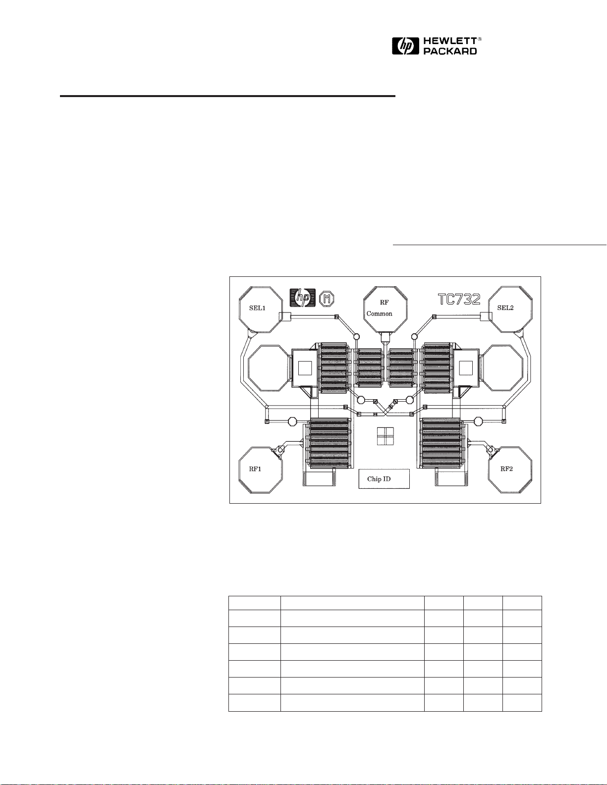
RF
COMMON
RF2
SEL2
Figure 1. HMMC-2007 Schematic.
Recommended Operating Conditions, T
=25°C
A
Select Line RF Path
RF IN to RF IN to
SEL1 SEL2 RF OUT2
+10 V - 1 0 V Isolated Low Loss
-10 V +10 V Low Loss Isolated
SEL1
RF OUT1
RF1
7-29
Page 5

HMMC-2007 Typical Performance
0
-1.0
-2.0
-3.0
INSERTION LOSS (dB)
-4.0
S
21-ON
, S
31-ON
0
-20
-40
-60
ISOLATION (dB)
-80
S
21-OFF
, S
31-OFF
0
-10
-20
-30
-40
INPUT RETURN LOSS (dB)
S
11
-5.0
0510
FREQUENCY (GHz)
Figure 2. Insertion Loss
[1]
vs.
Frequency.
0
-10
-20
-30
-40
OUTPUT RETURN LOSS (dB)
-50
0510
Figure 5. Output Return Loss
S
33
S
FREQUENCY (GHz)
22
[1]
vs.
Frequency.
-100
0510
FREQUENCY (GHz)
Figure 3. Input-to-Output Isolation
vs. Frequency.
0
-1
-2
-3
-4
GAIN COMPRESSION (dB)
-5
10 20 302515
POWER INPUT (dBm)
10 MHz
Figure 6. Gain Compression vs.
Power Input.
Note:
1. Data taken with the device mounted in modular breadboard package.
1 GHz
-50
0510
FREQUENCY (GHz)
[1]
Figure 4. Input Return Loss
[1]
vs.
Frequency.
7-30
Page 6

563
97
480
863
960
660
97
0
97
0
Figure 6. HMMC-2007 Bonding Pad Locations. (Dimensions in micrometers)
Note:
All compression data measured in an individual device mounted in an HP83040
Series Modular Microcircuit Package @ T
case
= 25° C.
97
863
This data sheet contains a variety of typical and guaranteed performance data. The
information supplied should not be interpreted as a complete list of circuit specifications. In this data sheet the term typical refers to the 50th percentile performance. For
additional information contact your local HP sales representative.
7-31
 Loading...