

Page 1
'99
new!
MICROWAVE CORPORATION
GaAS MMIC SMT LOW DISTORTION T/R SWITCH DC - 2.5 GHz
HMC154S8
7
FEBRUARY 2001
Features
HIGH THIRD ORDER INTERCEPT: +60 dBm
SINGLE POSITIVE SUPPLY: +3 TO +10V
HIGH RF POWER CAPABILITY
TTL/CMOS CONTROL
V01.0700
General Description
The HMC154S8 is a low-cost SPDT switch
in an 8-lead SOIC package for use in transmit-receive applications which require very
low distortion at high signal power levels.
The device can control signals from DC to
2.5 GHz and is especially suited for 900MHz
and 1.8-2.2 GHz applications. The design
provides exceptional intermodulation performance; providing a +60dBm third order
intercept at 8 Volt bias. RF1 or RF2 is a
reflective short when "Off". On-chip circuitry
allows single positive supply operation at
very low DC current with control inputs compatible with CMOS and most TTL logic families.
Guaranteed Performance, Vdd = +5 Vdc, 50 Ohm System, -40 to +85 deg C
retemaraP ycneuqerF .niM .pyT .xaM stinU
SWITCHES
ssoLnoitresnI
SPDT
SMT
12 Elizabeth Drive, Chelmsford, MA 01824 Phone: 978-250-3343 Fax: 978-250-3373 Web Site: www.hittite.com
7 - 16
noitalosI
ssoLnruteR
lortnoCV8/0noisserpmoCBd1rofrewoPtupnI
lortnoCV8/0tpecretnIredrOdrihTtupnI
scitsiretcarahCgnihctiwS
)FR%09/01(LLAFt,ESIRt
)FR%09/01otLTC%05(FFOt,NOt
zHG0.1-CD
zHG0.2-CD
zHG5.2-CD
zHG0.1-CD
zHG0.2-CD
zHG5.2-CD
zHG0.1-CD
zHG0.2-CD
zHG5.2-CD
zHG0.1-5.0
zHG0.2-5.0
zHG0.1-5.0
zHG0.2-5.0
zHG5.2-CD
22
91
51
02
41
01
53
43
55
45
5.0
7.0
0.1
52
22
81
03
81
31
93
83
06
06
01
42
7.0
9.0
3.1
Bd
Bd
Bd
Bd
Bd
Bd
Bd
Bd
Bd
mBd
mBd
sn
sn
Page 2
MICROWAVE CORPORATION
HMC154S8 SMT LOW DISTORTION T/R SWITCH DC - 2.5 GHz
new!
HMC154S8
'99
V01.0700
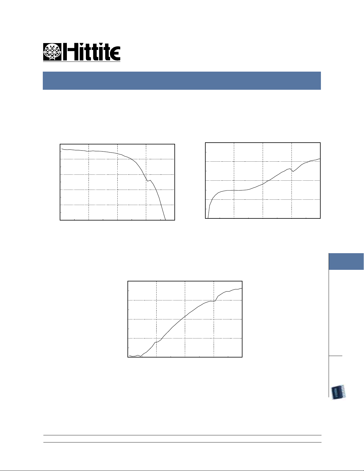
Insertion Loss
0
-1
-2
-3
-4
INSERTION LOSS (dB)
-5
01234
FREQUENCY (GHz)
Return Loss
FEBRUARY 2001
Isolation
0
-10
-20
ISOLATION (dB)
-30
-40
01 234
FREQUENCY (GHz)
7
0
-10
-20
-30
RETURN LOSS (dB)
-40
01234
FREQUENCY (GHz)
12 Elizabeth Drive, Chelmsford, MA 01824 Phone: 978-250-3343 Fax: 978-250-3373 Web Site: www.hittite.com
7 - 17
SWITCHES
SPDT
SMT
Page 3

'99
new!
MICROWAVE CORPORATION
HMC154S8 SMT LOW DISTORTION T/R SWITCH DC - 2.5 GHz
FEBRUARY 2001
Input Power for 0.1 and 1.0 dB
Compression vs Bias Voltage
45
1db at 1900MHz
40
35
30
COMPRESSION (dBm)
25
2 4 6 8 10 12
BIAS (Volts)
1dB at 900MHz
0.1dB at 900MHz
0.1dB at 1900MHz
HMC154S8
Input Third Order Intercept
vs Bias Voltage
65
60
55
50
IP3 (dBm)
45
40
35
2 4 6 8 10 12
900MHz
1900MHz
BIAS (Volts)
V01.0700
Compression vs Bias Voltage
7
SWITCHES
SPDT
Caution: Do not operate in 1dB compression at power levels above +35dBm and do
not "hot switch" power levels greater than +23 dBm (Vdd = +5V).
SMT
zHM009tareirraC zHM0091tareirraC
saiB
ddV
)stloV( )mBd( )mBd( )mBd( )mBd(
372136203
403439233
523631353
863935383
0173046393
rewoPtupnI
Bd1.0rof
noisserpmoC
rewoPtupnI
Bd1rof
noisserpmoC
rewoPtupnI
Bd1.0rof
noisserpmoC
Distortion vs Bias Voltage
zHM009tareirraCttaW1 zHM0091tareirraCttaW1
rewoPtupnI
Bd1rof
noisserpmoC
ddV
3341754248755
4845855648856
5350965157885
8060985060995
01060995060906
drihT
saiB
redrO
tpecretnI
)stloV( )mBd( )mBd( )cBd( )mBd( )mBd( )cBd(
dnoceS
redrO
dnoceS
drihT
-inomraH
tpecretnI
c
redrO
dnoceS
redrO
tpecretnI
-ecretnI
tp
dnoceS
cinomraH
12 Elizabeth Drive, Chelmsford, MA 01824 Phone: 978-250-3343 Fax: 978-250-3373 Web Site: www.hittite.com
7 - 18
Page 4

MICROWAVE CORPORATION
HMC154S8 SMT LOW DISTORTION T/R SWITCH DC - 2.5 GHz
new!
HMC154S8
'99
V01.0700
Functional Diagram
GND
RF2 GND
A
B
RF1
RF
Vdd
Absolute Maximum Ratings
)ddV(egnaRegatloVsaiBcdV21+ot2.0-
)B&A(egnaRegatloVlortnoCcdVddV+ot2.0-
erutarepmeTegarotSCged051+ot56-
erutarepmeTgnitarepOCged58+ot04-
Outline
PIN 8
0.188/0.196
(4.78/4.98)
GND
RF2 GND
RF1
T ruth Table
*Control Input Voltage Tolerances are ± 0.2 Vdc
saiB *tupnIlortnoC
ddV
A
)cdV(
300 0351-51-FFOFFO
30 ddV5252-0NOFFO
3ddV0 52052-FFONO
500 01155-55-FFOFFO
50 ddV511001-51-NOFFO
5ddV0 511
0100 083091-091-FFOFFO
010 ddV594572-
01ddV0 594
5ddV-ddV006006-522NOFFO
5ddVddV-006522006-FFONO
LOT NUMBER
B
)cdV(
saiB
ddvI
)cdV(
)Au(
lortnoC
tnerruC
al
)Au(
-51
-022
lortnoC
tnerruC
tnerruC
bl
)Au(
001-FFONO
-022
572-FFONO
FEBRUARY 2001
etatShtaPlangiS
1FRotFR 2FRotFR
NOFFO
7
DATE CODE
0.150/0.157
(3.81/4.00) (5.82/6.20)
0.229/0.244
HMC154S8
A
PIN 1
0.054/0.068
(1.37/1.73)
0.050
(1.27)
TYP
1) MATERIAL:
A) PACKAGE BODY: LOW STRESS INJECTION MOLDED PLASTIC,
SILICA & SILICONE IMPREGNATED
B) LEADFRAME MATERIAL: COPPER ALLOY
2 . PLATING: LEAD-TIN SOLDER PLATE
3. DIMENSIONS ARE IN INCHES (MILLIMETERS)
UNLESS OTHERWISE SPECIFIED TOLERANCE ARE ±0.005 (±0.13)
B
0.014/0.018
(0.36/0.46)
TYP
RF
Vdd
0.004/0.009
3 Deg / 8 Deg
NNNNN
0.016
MIN TYP
(0.41)
YY= YEAR
WW= WEEK
YYWW
PIN 1 (REF)
0.007/0.009
(0.18/0.25)
TYP
12 Elizabeth Drive, Chelmsford, MA 01824 Phone: 978-250-3343 Fax: 978-250-3373 Web Site: www.hittite.com
7 - 19
SWITCHES
SPDT
SMT
Page 5

'99
new!
MICROWAVE CORPORATION
HMC154S8 SMT LOW DISTORTION T/R SWITCH DC - 2.5 GHz
FEBRUARY 2001
Typical Application Circuit for HMC154S8
RF2
GND
Pin 1
A
+Vdd
B
HMC154S8
V01.0700
RF1
GND
Vdd
Notes:
7
1. Set logic gate and switch Vdd = +3V to +5V and use HCT series logic to provide a TTL driver interface.
2. Control inputs A/B can be driven directly with CMOS logic (HC) with Vdd of 3 to 8 Volts applied to the CMOS logic gates and
to pin 4 of the RF switch.
3. DC Blocking capacitors are required for each RF port as shown. Capacitor value determines lowest frequency of operation.
4. Highest RF signal power capability is achieved with V set to +10V. The switch will operate properly (but at lower RF
power capability) at bias voltages down to +3V.
SWITCHES
SPDT
SMT
CTL
RF
74HC04 or
74HCT04
12 Elizabeth Drive, Chelmsford, MA 01824 Phone: 978-250-3343 Fax: 978-250-3373 Web Site: www.hittite.com
7 - 20
Page 6

MICROWAVE CORPORATION
HMC154S8 SMT LOW DISTORTION T/R SWITCH DC - 2.5 GHz
new!
HMC154S8
'99
V01.0700
FEBRUARY 2001
Evaluation Circuit Board
The circuit board used in the final application should use RF circuit design techniques. Signal lines should
have 50 ohm impedance while the package ground leads should be connected directly to the ground plane
similar to that shown below. A sufficient number of VIA holes should be used to connect the top and bottom
ground planes. The evaluation circuit board as shown is available from Hittite upon request.
7
Evaluation Circuit Board Layout Design Details
Layout Technique Grounded Co-Planar Waveguide (GCPW)
Material FR4
Dielectric Thickness 0.028" (0.71 mm)
50 Ohm Line Width 0.037" (0.94 mm)
Gap to Ground Edge 0.010" (0.25 mm)
Ground VIA Hole Diameter 0.014" (0.36 mm)
Connectors SMA-F ( EF - Johnson P/N 142-0701-806)
12 Elizabeth Drive, Chelmsford, MA 01824 Phone: 978-250-3343 Fax: 978-250-3373 Web Site: www.hittite.com
7 - 21
SWITCHES
SPDT
SMT
 Loading...