

Page 1
March 1998
HI7191
24-Bit, High Precision,
Sigma Delta A/D Converter
Features
• 22-Bit Resolution with No Missing Code
• 0.0007% Integral Non-Linearity (Typ)
• 20mV to ±2.5V Full Scale Input Ranges
• Internal PGIA with Gains of 1 to 128
• Serial Data I/O Interface, SPI Compatible
• Differential Analog and Reference Inputs
• Internal or System Calibration
• -120dB Rejection of 60/50Hz Line Noise
• Settling Time of 4 Conversions (Max) for a Step Input
Applications
• Process Control and Measurement
• Industrial Weight Scales
• Part Counting Scales
• Laboratory Instrumentation
• Seismic Monitoring
• Magnetic Field Monitoring
• Additional Reference Literature
- TB348 “HI7190/1 Negative Full Scale Error vs
Conversion Frequency”
- AN9504 “A Brief Intro to Sigma Delta Conversion”
- TB329 “Intersil Sigma Delta Calibration Technique”
- AN9505 “Using the HI7190 Evaluation Kit”
- TB331 “Using the HI7190 Serial Interface”
- AN9527 “Interfacing HI7190 to a Microcontroller”
- AN9532 “Using HI7190 in a Multiplexed System”
- AN9601 “Using HI7190 with a Single +5V Supply”
Description
The Intersil HI7191 is a monolithic instrumentation, sigma delta
A/D converter which operates from ±5V supplies. Both the signal and reference inputs are fully differential for maximum flexibility and performance. An internal Programmable Gain
Instrumentation Amplifier (PGIA) provides input gains from 1 to
128 eliminating the need for external pre-amplifiers. The ondemand converter auto-calibrate function is capable of removing offset and gain errors existing in external and internal circuitry. The on-board user programmable digital filter provides
over -120dB of 60/50Hz noise rejection and allows fine tuning
of resolution and conversion speed ov er a wide dynamic range .
The HI7191 and HI7191 are functionally the same device so all
discussion will refer to the HI7191 for simplicity.
The HI7191 contains a serial I/O port and is compatible with
most synchronous transfer formats including both the Motorola 6805/11 series SPI and Intel 8051 series SSR protocols.
A sophisticated set of commands gives the user control over
calibration, PGIA gain, device selection, standby mode, and
several other features. The On-chip Calibration Registers
allow the user to read and write calibration data.
Ordering Information
TEMP.
PART NUMBER
HI7191IP -40 to 85 20 Ld PDIP E20.3
HI7191IB -40 to 85 20 Ld SOIC M20.3
HI7190EVAL Evaluation Kit
RANGE (oC) PACKAGE
PKG.
NO.
Pinout
HI7191
(PDIP, SOIC)
TOP VIEW
1
SCLK
SDO
2
SDIO
3
4
CS
5
DRDY
6
DGND
7
AV
SS
8
V
RLO
9
V
RHI
10
V
CM
CAUTION: These devices are sensitive to electrostatic discharge; follow proper IC Handling Procedures.
http://www.intersil.com or 407-727-9207
| Copyright © Intersil Corporation 1999
1897
20
19
18
17
16
15
14
13
12
11
MODE
SYNC
RESET
OSC
1
OSC
2
DV
DD
AGND
AV
DD
V
INHI
V
INLO
File Number 4138.3
Page 2
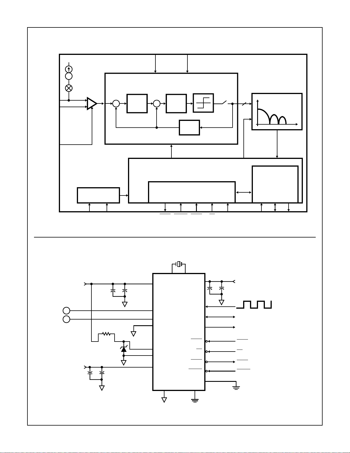
Functional Block Diagram
HI7191
V
V
INHI
INLO
V
CM
AV
DD
TRANSDUCER
BURN-OUT
CURRENT
PGIA
CLOCK
GENERATOR
V
RHI
REFERENCE
INPUTS
V
RLO
∑ − ∆
MODULATOR
∑
∫∫
∑
1-BIT
D/A
CONTROL AND SERIAL INTERFACE UNIT
CONTROL REGISTER
DIGITAL FILTER
1
SERIAL INTERFACE
UNIT
OSC1OSC
2
Typical Application Schematic
INPUT
INPUT
+5V
+
-
REFERENCE
-5V
0.1µF
R
+
+
0.1uF
1
+2.5V
4.7µF
4.7µF
DRDY RESET SYNC CS MODE S
10MHz
17 16
AV
V
INHI
V
INLO
V
CM
V
RHI
V
RLO
AV
AGND
DD
SS
OSC1OSC
14 6
13
12
11
10
9
8
7
2
RESET
MODE
DGND
DV
DD
SCLK
SDIO
SDO
SYNC
CS
DRDY
15
0.1µF
1
3
2
19
4
5
18
20
+
4.7µF
+5V
DATA I/O
DATA OUT
SYNC
CS
DRDY
RESET
CLK
SDIO SDO
1898
Page 3
HI7191
Absolute Maximum Ratings Thermal Information
Supply Voltage
AVDD to AGND . . . . . . . . . . . . . . . . . . . . . . . . . . . . . . . . . . .+5.5V
AVSS to AGND . . . . . . . . . . . . . . . . . . . . . . . . . . . . . . . . . . . -5.5V
DVDD to DGND. . . . . . . . . . . . . . . . . . . . . . . . . . . . . . . . . . +5.5V
DGND to AGND . . . . . . . . . . . . . . . . . . . . . . . . . . . . . . . . . ±0.3V
Analog Input Pins . . . . . . . . . . . . . . . . . . . . . . . . . . . . AVSS to AV
Digital Input, Output and I/O Pins. . . . . . . . . . . . . . . DGND to DV
ESD Tolerance (No Damage)
Human Body Model . . . . . . . . . . . . . . . . . . . . . . . . . . . . . . . 500V
Machine Model . . . . . . . . . . . . . . . . . . . . . . . . . . . . . . . . . . +100V
Charged Device Model . . . . . . . . . . . . . . . . . . . . . . . . . . . . 1000V
Operating Conditions
Temperature Range . . . . . . . . . . . . . . . . . . . . . . . . . . -40oC to 85oC
CAUTION: Stresses above those listed in “Absolute Maximum Ratings” may cause permanent damage to the device. This is a stress only rating and operation
of the device at these or any other conditions above those indicated in the operational sections of this specification is not implied.
Thermal Resistance (Typical, Note 1) θJA (oC/W)
PDIP Package. . . . . . . . . . . . . . . . . . . . . . . . . . . . . 125
SOIC Package. . . . . . . . . . . . . . . . . . . . . . . . . . . . . 100
Maximum Junction Temperature
Plastic Packages. . . . . . . . . . . . . . . . . . . . . . . . . . . . . . . . .150oC
DD
Maximum Storage Temperature Range . . . . . . . . . .-65oC to 150oC
DD
Maximum Lead Temperature (Soldering, 10s) . . . . . . . . . . . . 300oC
(SOIC - Lead Tips Only)
Electrical Specifications AV
= +5V, AVSS = -5V, DVDD = +5V, V
DD
= +2.5V, V
RHI
= AGND = 0V, VCM = AGND,
RLO
PGIA Gain = 1, OSCIN = 10MHz, Bipolar Input Range Selected, fN = 10Hz
PARAMETER TEST CONDITIONS MIN TYP MAX UNITS
SYSTEM PERFORMANCE
Integral Non-Linearity, INL End Point Line Method (Notes 3, 5, 6) - ±0.0007 ±0.0015 %FS
Differential Non-Linearity (Note 2) No Missing codes to 22-Bits LSB
Offset Error, V
OS
Offset Error Drift V
Full Scale Error, FSE V
Noise, e
N
Common Mode Rejection Ratio, CMRR V
See Table 1 - -- -
INHI
INHI
= V
- V
(Notes 3, 8) - 1 - µV/oC
INLO
= +2.5V (Notes 3, 5, 8, 10) - - - -
INLO
See Table 1 - - - -
CM
= 0V, V
INHI
= V
from -2V to +2V -70 - dB
INLO
Normal Mode 50Hz Rejection Filter Notch = 10Hz, 25Hz, 50Hz (Note 2) -120 - - dB
Normal Mode 60Hz Rejection Filter Notch = 10Hz, 30Hz, 60Hz (Note 2) -120 - - dB
Step Response Settling Time - 2 4 Conversions
ANALOG INPUTS
Input Voltage Range Unipolar Mode (Note 9) 0 - V
Input Voltage Range Bipolar Mode (Note 9) - V
Common Mode Input Range (Note 2) AV
Input Leakage Current, I
Input Capacitance, C
Reference Voltage Range, V
(V
= V
RHI
- V
REF
RLO
IN
IN
REF
)
Transducer Burn-Out Current, I
VIN = AVDD (Note 2) - - 1.0 nA
BO
REF
SS
- 5.0 -pF
2.5 - 5 V
- 200 - nA
-V
-AVDDV
REF
REF
V
V
CALIBRATION LIMITS
Positive Full Scale Calibration Limit - - 1.2(V
Negative Full Scale Calibration Limit - - 1.2(V
Offset Calibration Limit - - 1.2(V
Input Span 0.2(V
/Gain) - 2.4(V
REF
/Gain) -
REF
/Gain) -
REF
/Gain) -
REF
/Gain) -
REF
DIGITAL INPUTS
Input Logic High Voltage, V
Input Logic Low Voltage, V
Input Logic Current, I
I
IH
IL
(Note 11) 2.0 - - V
- - 0.8 V
VIN = 0V, +5V - 1.0 10 µA
1899
Page 4
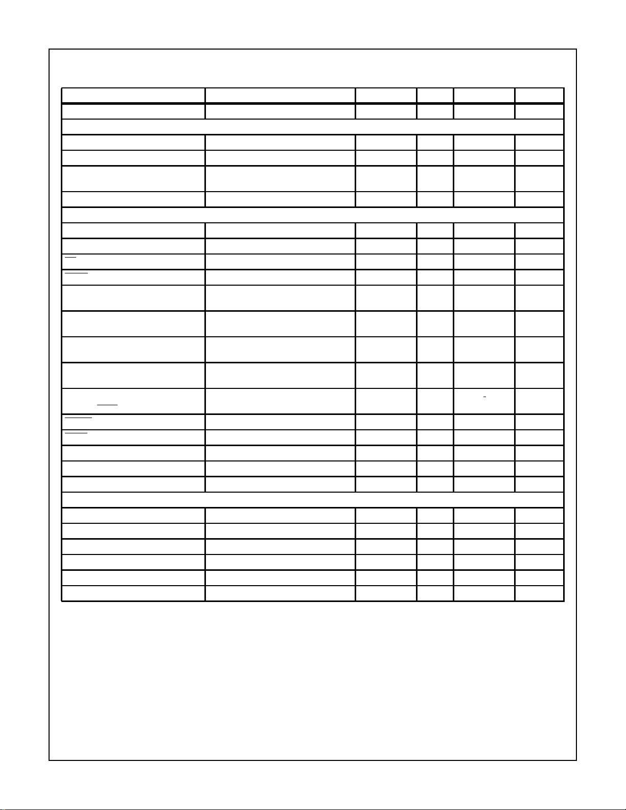
HI7191
Electrical Specifications AV
= +5V, AVSS = -5V, DVDD = +5V, V
DD
= +2.5V, V
RHI
= AGND = 0V, VCM = AGND,
RLO
PGIA Gain = 1, OSCIN = 10MHz, Bipolar Input Range Selected, fN = 10Hz (Continued)
PARAMETER TEST CONDITIONS MIN TYP MAX UNITS
Input Capacitance, C
IN
VIN = 0V - 5.0 - pF
DIGITAL OUTPUTS
Output Logic High Voltage, V
Output Logic Low Voltage, V
OH
OL
Output Three-State Leakage Current,
I
OZ
Digital Output Capacitance, C
OUT
I
= -100µA (Note 7) 2.4 - - V
OUT
I
= 3mA (Note 7) - - 0.4 V
OUT
V
= 0V, +5V (Note 7) -10 1 10 µA
OUT
-10- pF
TIMING CHARACTERISTICS
SCLK Minimum Cycle Time, t
SCLK Minimum Pulse Width, t
CS to SCLK Precharge Time, t
SCLK
SCLKPW
PRE
200 - - ns
50 - - ns
50 - - ns
DRDY Minimum High Pulse Width (Notes 2, 7) 500 - - ns
Data Setup to SCLK Rising Edge
(Write), t
DSU
Data Hold from SCLK Rising Edge
(Write), t
DHLD
Data Read Access from Instruction
Byte Write, t
ACC
Read Bit Valid from SCLK Falling Edge,
t
DV
Last Data Transfer to Data Ready
Inactive,t
DRDY
(Note 7) - - 40 ns
(Note 7) - - 40 ns
(Note 7) - 35 -ns
50 - - ns
0-- ns
RESET Low Pulse Width (Note 2) 100 - - ns
SYNC Low Pulse Width (Note 2) 100 - - ns
Oscillator Clock Frequency (Note 2) 0.1 - 10 MHz
Output Rise/Fall Time (Note 2) - - 30 ns
Input Rise/Fall Time (Note 2) - - 1 µs
POWER SUPPLY CHARACTERISTICS
IAV
DD
IAV
SS
IDV
DD
Power Dissipation, Active PD
Power Dissipation, Standby PD
SCLK = 4MHz - - 3.0 mA
A
SB = ‘0’ - 15 30 mW
SB = ‘1’ - 5 - mW
S
- - 1.5 mA
- - 1.5 mA
PSRR (Note 3) - -70 - dB
NOTES:
1. θJA is measured with the component mounted on an evaluation PC board in free air.
2. Parameter guaranteed by design or characterization, not production tested.
3. Applies to both bipolar and unipolar input ranges.
4. These errors can be removed by re-calibrating at the desired operating temperature.
5. Applies after system calibration.
6. Fully differential input signal source is used.
7. See Load Test Circuit, Figure 10, R1 = 10kΩ, CL = 50pF.
8. 1 LSB = 298nV at 24 bits for a Full Scale Range of 5V.
9. V
= V
RHI
- V
RLO
REF
10. These errors are on the order of the output noise shown in Table 1.
11. All inputs except OSC1. The OSC1 input VIH is 3.5V minimum.
1900
Page 5
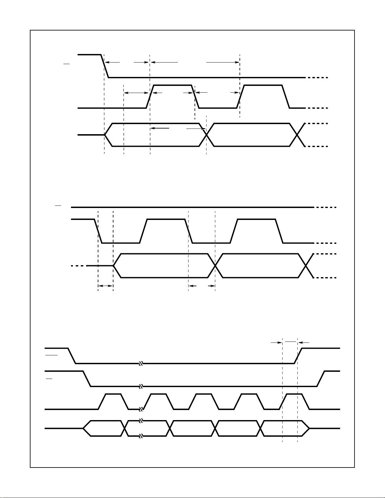
Timing Diagrams
CS
SCLK
SDIO
HI7191
t
t
DHLD
SCLK
t
SCLKPW
t
PRE
t
DSU
1ST BIT 2ND BIT
t
SCLKPW
FIGURE 1. DATA WRITE TO HI7191
SCLK
SDIO
SDO
DRDY
CS
CS
t
ACC
1ST BIT 2ND BIT
t
DV
FIGURE 2. DATA READ FROM HI7191
t
DRDY
SCLK
SDIO
87651
FIGURE 3. DATA READ FROM HI7191
1901
Page 6
HI7191
Pin Descriptions
20 LEAD
DIP, SOIC PIN NAME DESCRIPTION
1 SCLK Serial Interface Clock. Synchronizes serial data transfers. Data is input on the rising edge and output on the
falling edge.
2 SDO Serial Data OUT. Serial data is read from this line when using a 3-wire serial protocol such as the
Motorola Serial Peripheral Interface.
3 SDIO Serial Data IN or OUT. This line is bidirectional programmable and interfaces directly to the Intel Standard Serial
Interface using a 2-wire serial protocol.
4 CS Chip Select Input. Used to select the HI7191 for a serial data transfer cycle. This line can be tied to DGND.
5 DRDY An Active Low Interrupt indicating that a new data word is available for reading.
6 DGND Digital Supply Ground.
7AVSSNegative Analog Power Supply (-5V).
8V
RLO
9V
10 V
11 V
12 V
INLO
INHI
13 AV
14 AGND Analog Supply Ground.
15 DV
16 OSC2Used to connect a crystal source between OSC1 and OSC2. Leave open otherwise.
17 OSC1Oscillator Clock Input for the device. A crystal connected between OSC1 and OSC2will provide a clock to the
18 RESET Active Low Reset Pin. Used to initialize the HI7191 registers, filter and state machines.
19 SYNC Active Low Sync Input. Used to control the synchronization of a number of HI7191s . A logic ‘0’ initializes the converter .
20 MODE Mode Pin. Used to select between Synchronous Self Clocking (Mode = 1) or Synchronous External Clocking
External Reference Input. Should be negative referenced to V
External Reference Input. Should be positive referenced to V
RHI
Common Mode Input. Should be set to halfway between AVDD and AVSS.
CM
RHI
RLO
.
.
Analog Input LO. Negative input of the PGIA.
Analog Input HI. Positive input of the PGIA. The V
input is connected to a current source that can be used to check
INHI
the condition of an external transducer. This current source is controlled via the Control Register.
Positive Analog Power Supply (+5V).
DD
Positive Digital Supply (+5V).
DD
device, or an external oscillator can drive OSC1. The oscillator frequency should be 10MHz (Typ).
(Mode = 0) for the Serial Port.
Load Test Circuit
ESD Test Circuits
R
1
±
V
C
R
2
DUT
ESD
FIGURE 5A.
DUT
HUMAN BODY
= 100pF
C
ESD
R1 = 10MΩ
R2 = 1.5kΩ
MACHINE MODEL
C
= 200pF
ESD
R1 = 10MΩ
= 0Ω
R
2
V
1
R
1
CL (INCLUDES STRAY
CAPACITANCE)
FIGURE 4.
±
V
R
1
DUT
R
2
DIELECTRIC
CHARGED DEVICE MODEL
R1 = 1GΩ
R2 = 1Ω
FIGURE 5B.
1902
Page 7
TABLE 1. NOISE PERFORMANCE WITH INPUT CONNECTED TO ANALOG GROUND
P-P NOISE
HERTZ SNR ENOB
GAIN = 1
10 132.3 21.7 9.8 1.5
25 129.5 21.2 13.6 2.1
30 127.7 20.9 16.6 2.5
50 126.3 20.7 19.5 3.0
60 125.6 20.6 21.2 3.2
100 122.4 20.0 30.7 4.6
250 107.7 17.6 166.7 25.3
500 98.1 16.0 505.3 76.6
1000 85.7 13.9 2101.8 318.5
2000 68.8 11.1 14661.6 2221.4
GAIN = 2
10 129.2 21.2 14.0 2.1
25 125.7 20.6 20.9 3.2
30 124.5 20.4 24.1 3.7
50 123.4 20.2 27.3 4.1
60 122.5 20.1 30.3 4.6
100 118.1 19.3 50.0 7.6
250 106.1 17.3 199.5 30.2
500 96.9 15.8 580.1 87.9
1000 84.4 13.7 2435.6 369.0
2000 67.8 11.0 16469.7 2495.4
GAIN = 4
10 125.9 20.6 20.5 3.1
25 123.1 20.1 28.4 4.3
30 121.8 19.9 32.8 5.0
50 119.9 19.6 40.9 6.2
60 119.9 19.6 40.9 6.2
100 116.1 19.0 63.2 9.6
250 105.7 17.3 209.7 31.8
500 96.6 15.8 597.8 90.6
1000 84.3 13.7 2469.5 374.2
2000 68.2 11.0 15656.1 2372.1
GAIN = 8
10 124.7 20.4 23.4 3.5
25 120.6 19.7 37.8 5.7
30 119.2 19.5 44.3 6.7
50 117.5 19.2 53.8 8.2
60 116.8 19.1 58.6 8.9
100 112.1 18.3 100.0 15.2
250 101.4 16.5 345.2 52.3
500 95.3 15.5 691.1 104.7
1000 83.1 13.5 2838.6 430.1
2000 68.3 11.1 15494.7 2347.7
(µV)
RMS NOISE
(µV)
HI7191
GAIN = 16
GAIN = 32
GAIN = 64
GAIN = 128
P-P NOISE
HERTZ SNR ENOB
10 120.1 19.7 39.8 6.0
25 114.8 18.8 73.4 11.1
30 113.5 18.6 85.1 12.9
50 111.0 18.1 114.4 17.3
60 109.6 17.9 134.0 20.3
100 105.5 17.2 214.8 32.5
250 95.2 15.5 699.1 105.9
500 89.1 14.5 1417.7 214.8
1000 83.5 13.6 2686.0 407.0
2000 62.6 10.1 30110.0 4562.1
10 113.2 18.5 88.8 13.5
25 109.0 17.8 142.7 21.6
30 108.2 17.7 157.4 23.8
50 104.7 17.1 235.8 35.7
60 105.0 17.1 227.8 34.5
100 102.3 16.7 310.5 47.0
250 93.4 15.2 861.1 130.5
500 87.1 14.2 1782.7 270.1
1000 78.2 12.7 4990.4 756.1
2000 57.0 9.2 57311.1 8683.5
10 106.7 17.4 186.2 28.2
25 102.9 16.8 288.4 43.7
30 101.9 16.6 325.8 49.4
50 98.5 16.1 479.8 72.7
60 98.9 16.1 459.8 69.7
100 96.3 15.7 620.2 94.0
250 85.5 13.9 2133.5 323.3
500 78.1 12.7 5025.0 761.4
1000 66.7 10.8 18693.5 2832.3
2000 50.5 8.1 120163.0 18206.5
10 101.1 16.5 356.5 54.0
25 96.0 15.7 638.3 96.7
30 95.2 15.5 704.8 106.8
50 93.2 15.2 882.2 133.7
60 92.2 15.0 996.7 151.0
100 91.4 14.9 1086.6 164.6
250 79.4 12.9 4346.4 658.5
500 71.8 11.6 10439.2 1581.7
1000 60.1 9.7 39923.0 6048.9
2000 44.8 7.1 233238.2 35339.1
(µV)
RMS NOISE
(µV)
1903
Page 8

HI7191
Definitions
Integral Non-Linearity, INL, is the maximum deviation of
any digital code from a straight line passing through the endpoints of the transfer function. The endpoints of the transfer
function are zero scale (a point 0.5 LSB below the first code
transition 000...000 and 000...001) and full scale (a point 0.5
LSB above the last code transition 111...110 to 111...111).
Differential Non-Linearity, DNL, is the deviation from the
actual difference between midpoints and the ideal difference
between midpoints (1 LSB) for adjacent codes. If this difference is equal to or more negative than 1 LSB, a code will be
missed.
Offset Error , V
from the ideal input voltage (V
be calibrated to the order of the noise level sho wn in Table 1.
Full Scale Error, FSE, is the deviation of the last code
transition from the ideal input full scale voltage
(V
-+V
IN
REF
to the order of the noise level shown in Table 1.
Input Span, defines the minimum and maximum input
voltages the device can handle while still calibrating properly
for gain.
Noise, e
, Table 1 shows the peak-to-peak and RMS noise
N
for typical notch and -3dB frequencies. The device programming was for bipolar input with a V
the input range is 5V. The analysis was performed on 100
conversions with the peak-to-peak output noise being the
difference between the maximum and minimum readings
over a rolling 10 conversion window . The equation to convert
the peak-to-peak noise data to ENOB is:
ENOB = Log
where: V
FS
CF = 6.6 (Imperical Crest Factor)
The noise from the part comes from two sources, the
quantization noise from the analog-to-digital conversion process and device noise. Device noise (or Wideband Noise) is
independent of gain and essentially flat across the frequency
spectrum. Quantization noise is ratiometric to input full scale
(and hence gain) and its frequency response is shaped by
the modulator.
Looking at Table 1, as the cutoff frequency increases the
output noise increases. This is due to more of the
quantization noise of the part coming through to the output
and, hence, the output noise increases with increasing 3dB frequencies. For the lower notch settings, the output
noise is dominated by the device noise and, hence, altering
the gain has little effect on the output noise. At higher notch
frequencies, the quantization noise dominates the output
noise and, in this case, the output noise tends to decrease
with increasing gain.
Since the output noise comes from two sources, the effectiv e
resolution of the device (i.e., the ratio of the input full scale to
the output RMS noise) does not remain constant with
increasing gain or with increasing bandwidth. It is possible to
, is the deviation of the first code transition
OS
- 0.5 LSB). This error can
IN
/Gain - 1.5 LSB). This error can be calibrated
of +2.5V. This implies
REF
(VFS / V
2
= 5V, V
NRMS
NRMS
= V
)
NP-P
/ CF and
do post-filtering (such as brick wall filtering) on the data to
improve the ov erall resolution for a given -3dB frequency and
also to further reduce the output noise.
Circuit Description
The HI7191 is a monolithic, sigma delta A/D converter which
operates from ±5V supplies and is intended for
measurement of wide dynamic range, low frequency signals.
It contains a Programmable Gain Instrumentation Amplifier
(PGIA), sigma delta ADC, digital filter, bidirectional serial
port (compatible with many industry standard protocols),
clock oscillator, and an on-chip controller.
The signal and reference inputs are fully differential for
maximum flexibility and performance. Normally V
V
are tied to +2.5V and AGND respectively. This allows
RLO
for input ranges of 2.5V and 5V when operating in the unipolar and bipolar modes respectively (assuming the PGIA is
configured for a gain of 1). The internal PGIA provides input
gains from 1 to 128 and eliminates the need for external preamplifiers. This means the device will convert signals ranging from 0V to +20mV and 0V to +2.5V when operating in
the unipolar mode or signals in the range of ±20mV to ±2.5V
when operating in the bipolar mode.
The input signal is continuously sampled at the input to the
HI7191 at a clock rate set by the oscillator frequency and the
selected gain. This signal then passes through the sigma
delta modulator (which includes the PGIA) and emerges as
a pulse train whose code density contains the analog signal
information. The output of the modulator is fed into the sinc
digital low pass filter. The filter output passes into the
calibration block where offset and gain errors are removed.
The calibrated data is then coded (2’s complement, offset
binary or binary) before being stored in the Data Output
Register. The Data Output Register update rate is determined by the first notch frequency of the digital filter. This
first notch frequency is programmed into HI7191 via the
Control Register and has a range of 10Hz to 1.953kHz which
corresponds to -3dB frequencies of 2.62Hz and 512Hz
respectively.
Output data coding on the HI7191 is programmable via the
Control Register. When operating in bipolar mode, data output can be either 2’s complement or offset binary. In unipolar
mode output is binary.
The
DRDY signal is used to alert the user that new output
data is available. Converted data is read via the HI7191
serial I/O port which is compatible with most synchronous
transfer formats including both the Motorola 6805/11 series
SPI and Intel 8051 series SSR protocols. Data Integrity is
always maintained at the HI7191 output port. This means
that if a data read of conversion N is begun but not finished
before the next conversion (conversion N + 1) is complete,
the
DRDY line remains active (low) and the data being read
is not overwritten.
The HI7191 provides many calibration modes that can be
initiated at any time by writing to the Control Register. The
device can perform system calibration where external components are included with the HI7191 in the calibration loop
RHI
and
3
1904
Page 9

HI7191
or self-calibration where only the HI7191 itself is in the calibration loop. The On-chip Calibration Registers are
read/write registers which allow the user to read calibration
coefficients as well as write previously determined
calibration coefficients.
Circuit Operation
The analog and digital supplies and grounds are separate
on the HI7191 to minimize digital noise coupling into the
analog circuitry. Nominal supply voltages are AV
DV
= +5V, and AVSS = -5V. If the same supply is used
DD
for AV
rately decoupled to the AV
and DVDD it is imperative that the supply is sepa-
DD
and DVDD pins on the
DD
HI7191. Separate analog and digital ground planes should
be maintained on the system board and the grounds should
be tied together back at the power supply.
When the HI7191 is powered up it needs to be reset by pulling the
RESET line low. The reset sets the internal registers
of the HI7191 as shown in Table 2 and puts the part in the
bipolar mode with a gain of 1 and offset binary coding. The
filter notch of the digital filter is set at 30Hz while the I/O is
set up for bidirectional I/O (data is read and written on the
SDIO line and SDO is three-stated), descending byte order,
and MSB first data format. A self calibration is performed
before the device begins converting.
DRDY goes low when
valid data is available at the output.
TABLE 2. REGISTER RESET VALUES
REGISTER VALUE (HEX)
Data Output Register XXXX (Undefined)
Control Register 28B300
Offset Calibration Register Self Calibration Value
Positive Full Scale Calibration
Register
Negative Full Scale Calibration
Register
Self Calibration Value
Self Calibration Value
The configuration of the HI7191 is changed by writing new
setup data to the Control Register. Whenever data is written
to byte 2 and/or byte 1 of the Control Register the part
assumes that a critical setup parameter is being changed
which means that
DRDY goes high and the device is re-synchronized. If the configuration is changed such that the
device is in any one of the calibration modes, a new calibration is performed before normal conversions continue. If the
device is written to the conversion mode , a new calibration is
NOT performed (A new calibr ation is recommended any time
data is written to the Control Register.). In either case,
goes low when valid data is available at the output.
If a single data byte is written to byte 0 of the Control
Register, the device assumes the gain has NOT been
changed. It is up to the user to re-calibrate the device if the
gain is changed in this manner. For this reason it is
recommended that the entire Control Register be written
when changing the gain of the device. This ensures that the
DD
= +5V,
DRD Y
part is re-calibrated (if in a calibration mode) before the
DRDY output goes low indicating that valid data is available.
The calibration registers can be read via the serial interface
at any time. However, care must be taken when writing data
to the calibration registers. If the HI7191 is internally
updating any calibration register the user can not write to
that calibration register. See the Operational Modes section
for details on which calibration registers are updated for the
various modes.
Since access to the calibration registers is asynchronous to
the conversion process the user is cautioned that new
calibration data may not be used on the very next set of
“valid” data after a calibration register write. It is guaranteed
that the new data will take effect on the second set of output
data. Non-calibrated data can be obtained from the device
by writing 000000 (h) to the Offset Calibration Register,
800000 (h) to the Positive Full Scale Calibration Register,
and 800000 (h) to the Negative Full Scale Calibration Register. This sets the offset correction factor to 0 and the positive
and negative gain slope factors to 1.
If several HI7191s share a system master clock the
SYNC
pin can be used to synchronize their operation. A common
SYNC input to multiple devices will synchronize operation
such that all output registers are updated simultaneously. Of
course the
SYNC pin would normally be activated only after
each HI7191 has been calibrated or has had calibration
coefficients written to it.
The
SYNC pin can also be used to control the HI7191 when
an external multiplexer is used with a single HI7191. The
SYNC pin in this application can be used to guarantee a max-
imum settling time of 3 conversion periods when switching
channels on the multiplexer.
Analog Section Description
Figure 6 shows a simplified block diagram of the analog
modulator front end of a sigma delta A/D Converter. The
input signal V
this case) where the previous modulator output is subtracted
from it. The resulting signal is then integrated and the output
of the integrator goes into the comparator. The output of the
comparator is then fed back via a 1-bit DAC to the summing
junction. The feedback loop forces the average of the fed
back signal to be equal to the input signal V
V
IN
FIGURE 6. SIMPLE MODULATOR BLOCK DIAGRAM
comes into a summing junction (the PGIA in
IN
.
IN
PGIA INTEGRATOR COMPARATOR
+
∑
-
DAC
V
V
RHI
RLO
∫
+
-
1905
Page 10

HI7191
Analog Inputs
The analog input on the HI7191 is a fully differential input
with programmable gain capabilities. The input accepts both
unipolar and bipolar input signals and gains range from 1 to
128. The common mode range of this input is from AVSS to
AV
provided that the absolute value of the analog input
DD
voltage lies within the power supplies. The input impedance
of the HI7191 is dependent upon the modulator input sampling rate and the sampling rate varies with the selected
PGIA gain. Table 3 below shows the sampling rates and
input impedances for the different gain settings of the
HI7191. Note that this table is valid only for a 10MHz master
clock. If the input clock frequency is changed then the input
impedance will change accordingly. The equation used to
calculate the input impedance is:
ZIN = 1/(CIN x fS),
where C
is the nominal input capacitance (8pF) and fS is
in
the modulator sampling rate.
TABLE 3. EFFECTIVE INPUT IMPEDANCE vs GAIN
SAMPLING RATE
GAIN
1 78.125 1.6
2 156.25 0.8
4 312.5 0.4
8, 16, 32, 64, 128 625 0.2
(kHz)
INPUT IMPEDANCE
(MΩ)
Bipolar/Unipolar Input Ranges
The input on the HI7191 can accept either unipolar or bipolar
input voltages. Bipolar or unipolar options are chosen by programming the B/
U bit of the Control Register. Programming
the part for either unipolar or bipolar operation does not
change the input signal conditioning.
The inputs are differential, and as a result are referenced to
the voltage on the V
input. For example, if V
INLO
INLO
is
+1.25V and the HI7191 is configured for unipolar operation
with a gain of 1 and a V
on the V
input is +1.25V to +3.75V. If V
INLO
of +2.5V, the input voltage range
REF
INLO
is +1.25V
and the HI7191 is configured for bipolar mode with gain of 1
and a V
of +2.5V, the analog input range on the V
REF
INHI
input is -1.25V to +3.75V.
Programmable Gain Instrumentation Amplifier
The Programmable Gain Instrumentation Amplifier allows the
user to directly interface low le v el sensors and bridges directly
to the HI7191. The PGIA has 4 selectable gain options of 1, 2,
4, 8 which are implemented by multiple sampling of the input
signal. Input signals can be gained up further to 16, 32, 64 or
128. These higher gains are implemented in the digital section
of the design to maintain a high signal to noise ratio through
the front end amplifiers. The gain is digitally programmable in
the Control Register via the serial interface. For optimum
PGIA performance the V
pin should be tied to the mid point
CM
of the analog supplies.
Differential Reference Input
The reference inputs of the of the HI7191, V
RHI
and V
RLO
provide a differential reference input capability. The nominal
differential voltage (V
common mode voltage cab be anywhere between AV
AV
. Larger values of V
DD
REF
= V
RHI
REF
- V
) is +2.5V and the
RLO
can be used without
SS
and
degradation in performance with the maximum reference
voltage being V
= +5V. Smaller values of V
REF
REF
can also
be used but performance will be degraded since the LSB
size is reduced.
The full scale range of the HI7191 is defined as:
FSR
BIPOLAR
FSR
UNIPOLAR
and V
= 2 x V
= V
must always be greater than V
RHI
REF
REF
/GAIN
/GAIN
for proper
RLO
operation of the device.
The reference inputs provide a high impedance dynamic
load similar to the analog inputs and the effective input
impedance for the reference inputs can be calculated in the
same manner as it is for the analog input impedance. The
only difference in the calculation is that C
for the reference
IN
inputs is 10.67pF. Therefor, the input impedance range for
the reference inputs is from 149kΩ in a gain of 8 or higher
mode to 833kΩ in the gain of 1 mode.
V
Input
CM
The voltage at the V
input is the voltage that the internal
CM
analog circuitry is referenced to and should always be tied to
the midpoint of the AV
and AVSS supplies. This point
DD
provides a common mode input voltage for the internal operational amplifiers and must be driven from a low noise, low
impedance source if it is not tied to analog ground. Failure to
do so will result in degraded HI7191 performance. It is
recommended that V
operating off of AV
V
also determines the headroom at the upper and lower
CM
be tied to analog ground when
CM
= +5V and AVSS = -5V supplies.
DD
ends of the power supplies which is limited by the common
mode input range where the internal operational amplifiers
remain in the linear, high gain region of operation. The
HI7191 is designed to have a range of AV
AV
- 1.8V. Exceeding this range on the VCM pin will
DD
+1.8V < VCM <
SS
compromise the device performance.
Transducer Burn-Out Current Source
The V
input of the HI7191 contains a 500nA (Typ) current
INHI
source which can be turned on/off via the Control Register.
This current source can be used in checking whether a transducer has burnt-out or become open before attempting to take
measurements on that channel. When the current source is
turned on an additional offset will be created indicating the
presence of a transducer. The current source is controlled by
the BO bit (Bit 4) in the Control Register and is disabled on
power up. See Figure 8 for an applications circuit.
,
1906
Page 11

HI7191
HI7191
AV
DD
RATIOMETRIC
CONFIGURATION
LOAD CELL
FIGURE 7. BURN-OUT CURRENT SOURCE CIRCUIT
CURRENT
SOURCE
V
RHI
V
RLO
V
INHI
V
INLO
AV
SS
Digital Section Description
A block diagram of the digital section of the HI7191 is shown
in Figure 9. This section includes a low pass decimation filter, conversion controller, calibration logic, serial interface,
and clock generator.
MODULATOR
CLOCK
CALIBRATION
DIGITAL
FILTER
MODULATOR OUTPUT
FIGURE 8. DIGITAL SECTION BLOCK DIAGRAM
AND CONTROL
CLOCK
GENERATOR
SERIAL I/O
RESETSYNC
Digital Filtering
One advantage of digital filtering is that it occurs after the
conversion process and can remove noise introduced during
the conversion. It can not, however, remove noise present on
the analog signal prior to the ADC (which an analog filter
can).
One problem with the modulator/digital filter combination is
that excursions outside the full scale range of the device
could cause the modulator and digital filter to saturate. This
device has headroom built in to the modulator and digital filter which tolerates signal deviations up to 33% outside of the
full scale range of the device. If noise spikes can drive the
input signal outside of this extended range, it is recommended that an input analog filter is used or the overall input
signal level is reduced.
OSC
OSC
SDO
SDIO
SCLK
CS
DRDY
Low Pass Decimation Filter
The digital low-pass filter is a Hogenauer (sinc
3
) decimating
filter. This filter was chosen because it is a cost effective low
pass decimating filter that minimizes the need for internal
multipliers and extensive storage and is most effective when
used with high sampling or oversampling rates. Figure 10
shows the frequency characteristics of the filter where f
the -3dB frequency of the input signal and f
programmed notch frequency. The analog modulator sends
a one bit data stream to the filter at a rate of that is
determined by:
f
MODULATOR
f
MODULATOR
= f
/128
OSC
= 78.125kHz for f
OSC
= 10MHz.
The filter then converts the serial modulator data into 40-bit
words for processing by the Hogenauer filter. The data is
decimated in the filter at a rate determined by the CODE
word FP10-FP0 (programed by the user into the Control
Register) and the external clock rate. The equation is:
f
= f
NOTCH
/(512 x CODE).
OSC
The Control Register has 11 bits that select the filter cutoff
frequency and the first notch of the filter. The output data
update rate is equal to the notch frequency. The notch frequency sets the Nyquist sampling rate of the device while
the -3dB point of the filter determines the frequency spectrum of interest (f
through 2047 where 10 yields a 1.953kHz Nyquist rate.
2
1
The Hogenauer filter contains alias components that reflect
). The FP bits have a usable range of 10
S
around the notch frequency. If the spectrum of the frequency
of interest reaches the alias component, the data has been
aliased and therefore undersampled.
Filter Characteristics
Please note: We have recently discovered a performance
anomaly with the HI7191. The problem occurs when the
digital code for the notch filter is programmed within
certain frequencies. We believe the error is caused by
the calibration logic and the digital notch code NOT the
absolute frequency. The error is seen when the user
applies mid-scale (0V input, Bipolar mode). With this
input, the expected digital output should be mid-scale
(800000
erroneous negative full scale (000000
). Instead, there is a small probability, of an
h
)output. Refer to
h
Technical Brief TB348 for complete details.
The FP10 to FP0 bits programmed into the Control Register
determine the cutoff (or notch) frequency of the digital filter.
The allowable code range is 00A
. This corresponds to a
H
maximum and minimum cutoff frequency of 1.953kHz and
10Hz, respectively when operating at a clock frequency of
10MHz. If a 1MHz clock is used then the maximum and minimum cutoff frequencies become 195.3kHz and 1Hz, respectively. A plot of the (sinx/x)
3
digital filter characteristics is
shown in Figure 10. This filter provides greater than 120dB
of 50Hz or 60Hz rejection. Changing the clock frequency or
the programming of the FP bits does not change the shape
of the filter characteristics, it merely shifts the notch frequency. This low pass digital filter at the output of the con-
is the
N
is
C
1907
Page 12

HI7191
verter has an accompanying settling time for step inputs just
as a low pass analog filter does. New data takes between 3
and 4 conversion periods to settle and update on the serial
port with a conversion period t
0
-20
-40
-60
-80
AMPLITUDE (dB)
-100
-120
FIGURE 9. LOW PASS FILTER FREQUENCY CHARACTERISTICS
ALIAS BAND
f
C
fN±f
C
f
N
FREQUENCY (Hz)
being equal to 1/fN.
CONV
2f
N
3f
N
4f
N
Input Filtering
The digital filter does not provide rejection at integer multiples of the modulator sampling frequency. This implies that
there are frequency bands where noise passes to the output
without attenuation. For most cases this is not a problem
because the high oversampling rate and noise shaping characteristics of the modulator cause this noise to become a
small portion of the broadband noise which is filtered. However, if an anti-alias filter is necessar y a single pole RC filter
is usually sufficient.
If an input filter is used the user must be careful that the
source impedance of the filter is low enough not to cause
gain errors in the system. The DC input impedance at the
inputs is > 1GΩ but it is a dynamic load that changes with
clock frequency and selected gain. The input sample rate,
also dependent upon clock frequency and gain, determines
the allotted time for the input capacitor to charge. The addition of external components may cause the charge time of
the capacitor to increase beyond the allotted time. The result
of the input not settling to the proper value is a system gain
error which can be eliminated by system calibration of the
HI7191.
Clocking/Oscillators
The master clock into the HI7191 can be supplied by either a
crystal connected between the OSC
and OSC2 pins as
1
shown in Figure 11A or a CMOS compatible clock signal
connected to the OSC
pin as shown in Figure 11B. The
1
input sampling frequency, modulator sampling frequency, filter -3dB frequency, output update rate, and calibration time
are all directly related to the master clock frequency, f
OSC
For example, if a 1MHz clock is used instead of a 10MHz
clock, what is normally a 10Hz conversion rate becomes a
1Hz conversion rate. Lowering the clock frequency will also
lower the amount of current drawn from the power supplies.
Please note that the HI7191 specifications are written for a
10MHz clock only.
10MHz
1617
OSC
1
HI7191
FIGURE 10A.
10MHz
OSC
1
FIGURE 10B.
FIGURE 10. OSCILLATOR CONFIGURATIONS
OSC
CONNECTION
HI7191
2
NO
OSC
1617
2
Operational Modes
The HI7191 contains several operational modes including
calibration modes for cancelling offset and gain errors of
both internal and external circuitry. A calibration routine
should be initiated whenever there is a change in the ambient operating temperature or supply voltage. Calibration
should also be initiated if there is a change in the gain, filter
notch, bipolar, or unipolar input range. Non-calibrated data
can be obtained from the device by writing 000000 to the
Offset Calibration Register, 800000 (h) to the Positive Full
Scale Calibration Register, and 800000 (h) to the Negative
Full Scale Calibration Register. This sets the offset
correction factor to 0 and both the positive and negative gain
slope factors to 1.
The HI7191 offers several different modes of Self-Calibration
and System Calibration. For calibration to occur, the on-chip
microcontroller must convert the modulator output for three
different input conditions - “zero-scale,” “positive full scale,”
and “negative full scale”. With these readings, the HI7191
can null any offset errors and calculate the gain slope factor
for the transfer function of the converter. It is imperative that
the zero-scale calibration be performed before either of the
gain calibrations. However, the order of the gain calibrations
is not important.
The calibration modes are user selectable in the Control
Register by using the MD bits (MD2-MD0) as shown in
Ta bl e 6 .
DRDY will go low indicating that the calibration is
complete and there is valid data at the output.
.
1908
Page 13

HI7191
TABLE 4. HI7191 OPERATIONAL MODES
MD2 MD1 MD0 OPERATIONAL MODE
0 0 0 Conversion
0 0 1 Self Calibration (Gain of 1 only)
0 1 0 System Offset Calibration
0 1 1 System Positive Full Scale Calibration
1 0 0 System Negative Full Scale Calibration
1 0 1 System Offset/Internal Gain Calibration
(Gain of 1 only)
1 1 0 System Gain Calibration
1 1 1 Reserved
Conversion Mode
For Conversion Mode operation the HI7191 converts the differential voltage between V
into this mode it takes 3 conversion periods (3 x 1/f
INHI
and V
. From switching
INLO
N
) for
DRDY to go low and new data to be valid. No calibration
coefficients are generated when operating in Conversion
Mode as data is calibrated using the existing calibration
coefficients.
Self-Calibration Mode
Please note: Self-calibration is only valid when operating
in a gain of one. In addition, the offset and gain errors are
not reduced as with the full system calibration.
The Self-Calibration Mode is a three step process that
updates the Offset Calibration Register, the Positive Full
Scale Calibration Register, and the Negative Full Scale Calibration Register. In this mode an internal offset calibration is
done by disconnecting the external inputs and shorting the
inputs of the PGIA together. After 3 conversion periods the
Offset Calibration Register is updated with the value that
corrects any internal offset errors.
After the offset calibration is completed the Positive and
Negative Full Scale Calibration Registers are updated. The
inputs V
INHI
and V
are disconnected and the external
INLO
reference is applied across the modulator inputs. The
HI7191 then takes 3 conversion cycles to sample the data
and update the Positive Full Scale Calibration Register. Next
the polarity of the reference voltage across the modulator
input terminals is reversed and after 3 conversion cycles the
Negative Full Scale Calibration Register is updated. The
values stored in the Positive and Negative Full Scale
Calibration Registers correct for any internal gain errors in
the A/D transfer function. After 3 more conversion cycles the
DRDY line will activate signaling that the calibration is complete and valid data is present in the Data Output Register.
System Offset Calibration Mode
The System Offset Calibration Mode is a single step process
that allows the user to lump offset errors of external circuitry
and the internal errors of the HI7191 together and null them
out. This mode will convert the external differential signal
applied to the V
set Calibration Register.
inputs and then store that value in the Off-
IN
The user must apply the zero point
or offset voltage to the HI7191 analog inputs and allow the
signal to settle before selecting this mode.
sion periods the
DRDY line will activate signaling that the
After 4 conver-
calibration is complete and valid data is present in the Data
Output Register.
System Positive Full Scale Calibration Mode
The System Positive Full Scale Calibration Mode is a single
step process that allows the user to lump gain errors of
external circuitry and the internal errors of the HI7191
together and null them out. This mode will convert the external differential signal applied to the V
inputs and stores the
IN
converted value in the Positive Full Scale Calibration Register.
The user must apply the +Full Scale voltage to the
HI7191 analog inputs and allow the signal to settle before
selecting this mode.
After 4 conversion periods the DRDY
line will activate signaling the calibration is complete and
valid data is present in the Data Output Register.
System Negative Full Scale Calibration Mode
The System Negative Full Scale Calibration Mode is a
single-step process that allows the user to lump gain errors
of external circuitry and the internal errors of the HI7191
together and null them out. This mode will convert the external differential signal applied to the V
inputs and stores the
IN
converted value in the Negative Full Scale Calibration Register.
The user must apply the -Full Scale voltage to the
HI7191 analog inputs and allow the signal to settle before
selecting this mode.
After 4 conversion periods the DRDY
line will activate signaling the calibration is complete and
valid data is present in the Data Output Register.
System Offset/Internal Gain Calibration Mode
Please note: System Offset/Internal Gain is only valid
when operating in a gain of one. In addition, the offset and
gain errors are not reduced as with the full system calibration.
The System Offset/Internal Gain Calibration Mode is a single
step process that updates the Offset Calibration Register,
the Positive Full Scale Calibr ation Register, and the Negative
Full Scale Calibration Register. First the external differential
signal applied to the V
stored in the Offset Calibration Register.
inputs is converted and that value is
IN
The user must
apply the zero point or offset voltage to the HI7191 analog
inputs and allow the signal to settle before selecting this
mode.
After this is completed the Positive and Negative Full Scale
Calibration Registers are updated. The inputs V
INHI
and V
INLO
are disconnected and the external reference is switched in. The
HI7191 then takes 3 conversion cycles to sample the data and
update the Positive Full Scale Calibration Register. Next the
polarity of the reference voltage across the V
INHI
and V
INLO
terminals is reversed and after 3 conversion cycles the
Negative Full Calibration Register is updated. The values
stored in the Positive and Negative Full Scale Calibration
Registers correct for any internal gain errors in the A/D transfer
function. After 3 more conversion cycles, the DRDY line will
activate signaling that the calibration is complete and valid data
is present in the Data Output Register.
1909
Page 14

HI7191
System Gain Calibration Mode
The Gain Calibration Mode is a single step process that
updates the Positive and Negative Full Scale Calibration Registers. This mode will convert the external differential signal
applied to the V
inputs and then store that value in the Nega-
IN
tive Full Scale Calibration Register. Then the polarity of the
input is reversed internally and another conversion is performed. This conversion result is written to the Positive Full
Scale Calibration Register. The user must apply the +Full
Scale voltage to the HI7191 analog inputs and allow the signal
to settle before selecting this mode. After 1 more conversion
period the
DRDY line will activate signaling the calibration is
complete and valid data is present in the data output register.
Reserved
This mode is not used in the HI7191 and should not be
selected. There is no internal detection logic to keep this
condition from being selected and care should be taken not
to assert this bit combination.
Offset and Span Limits
There are limits to the amount of offset and gain which can
be adjusted out for the HI7191. For both bipolar and unipolar
modes the minimum and maximum input spans are
0.2xV
/GAIN and 1.2 x V
REF
/GAIN respectively.
REF
In the unipolar mode the offset plus the span cannot exceed
the 1.2 x V
value of 0.2 x V
V
/ GAIN. In bipolar mode the span is equidistant around
REF
/ GAIN limit. So, if the span is at its minimum
REF
/ GAIN, the offset must be less than 1 x
REF
the voltage used for the zero scale point. For this mode the
offset plus half the span cannot exceed 1.2 x V
the span is at ±0.2 x V
greater than ±2 x V
REF
/ GAIN, then the offset can not be
REF
/GAIN.
REF
/GAIN. If
Serial Interface
The HI7191 has a flexible, synchronous serial communication
port to allow easy interfacing to many industry standard microcontrollers and microprocessors. The serial I/O is compatible
with most synchronous transfer formats, including both the
Motorola 6805/11 SPI and Intel 8051 SSR protocols. The
Serial Interface is a flexible 2-wire or 3-wire hardw are interface
where the HI7191 can be configured to read and write on a
single bidirectional line (SDIO) or configured for writing on
SDIO and reading on the SDO line.
The interface is byte organized with each register byte
having a specific address and single or multiple byte transfers are supported. In addition, the interface allows flexibility
as to the byte and bit access order. That is, the user can
specify MSB/LSB first bit positioning and can access bytes
in ascending/descending order from any byte position.
The serial interface allows the user to communicate with 5
registers that control the operation of the device.
Data Output Register - a 24-bit, read only register
containing the conversion results.
Control Register - a 24-bit, read/write register containing
the setup and operating modes of the device.
Offset Calibration Register - a 24-bit, read/write register
used for calibrating the zero point of the converter or system.
Positive Full Scale Calibration Register - a 24-bit,
read/write register used for calibrating the Positive Full Scale
point of the converter or system.
Negative Full Scale Calibration Register - a 24-bit,
read/write register used for calibrating the Negative Full
Scale point of the converter or system.
Two clock modes are supported. The HI7191 can accept the
serial interface clock (SCLK) as an input from the system or
generate the SCLK signal as an output. If the MODE pin is
logic low the HI7191 is in external clocking mode and the
SCLK pin is configured as an input. In this mode the user
supplies the serial interface clock and all interface timing
specifications are synchronous to this input. If the MODE pin
is logic high the HI7191 is in self-clocking mode and the
SCLK pin is configured as an output. In self-clocking mode,
SCLK runs at F
= OSC1/8 and stalls high at byte
SCLK
boundaries. SCLK does NOT have the capability to stall low
in this mode. All interface timing specifications are
synchronous to the SCLK output.
Normal operation in self-clocking mode is as follows (See
Figure 13):
first SCLK transition output is delayed 29 OSC
the next rising OSC
stalls high for 28 OSC
CS is sampled low on falling OSC1 edges. The
cycles from
. SCLK transitions eight times and then
1
cycles. After this stall period is com-
1
1
pleted SCLK will again transition eight times and stall high.
This sequence will repeat continuously while
The extra OSC
cycle required when coming out of the CS
1
CS is active.
inactive state is a one clock cycle latency required to properly sample the
boundaries is 28 OSC
rising edge stall period of 32 OSC
The affects of
CS input. Note that the normal stall at byte
cycles thus giving a SCLK rising to
1
cycles.
1
CS on the I/O are different for self-clocking
mode (MODE = 1) than for external mode (MODE = 0). For
external clocking mode
CS inactive disables the I/O state
machine, effectively freezing the state of the I/O cycle. That
is, an I/O cycle can be interrupted using chip select and the
HI7191 will continue with that I/O cycle when re-enabled via
CS. SCLK can continue toggling while CS is inactive. If CS
goes inactive during an I/O cycle, it is up to the user to
ensure that the state of SCLK is identical when reactivating
CS as to what it was when CS went inactive. For read operations in external clocking mode, the output will go three-state
immediately upon deactivation of
CS.
For self-clocking mode (MODE = 1), the affects of CS are
different. If CS transitions high (inactive) during the period
when data is being transferred (any non stall time) the HI7191
will complete the data transfer to the byte boundary. That is,
once SCLK begins the eight transition sequence, it will always
complete the eight cycles. If CS remains inactive after the byte
has been transferred it will be sampled and SCLK will remain
stalled high indefinitely . If CS has returned to active lo w bef ore
the data byte transfer period is completed the HI7191 acts as
if CS was active during the entire transfer period.
1910
Page 15

HI7191
It is important to realize that the user can interrupt a data
transfer on byte boundaries. That is, if the Instruction Register calls for a 3 byte transf er and
CS is inactive after only one
byte has been transferred, the HI7191, when reactiv ated, will
continue with the remaining two bytes before looking for the
next Instruction Register write cycle.
Note that the outputs will NOT go three-state immediately upon
CS inactive for read operations in self-clocking mode. In the
case of CS going inactive during a read cycle the outputs
remain driving until after the last data bit is transferred. In the
case of CS inactive during the clock stall time it takes 1 OSC
cycle plus prop delay (Max) for the outputs to be disab led.
I/O Port Pin Descriptions
The serial I/O port is a bidirectional por t which is used to
read the data register and read or write the control register
and calibration registers. The port contains two data lines, a
synchronous clock, and a status flag. Figure 12 shows a
diagram of the serial interface lines.
DATA OUT
BIDIRECTIONAL DATA
PORT CLOCK
CHIP SELECT
DEVICE STATUS
SDO
SDIO
SCLK
CS
DRDY
MODECLOCK MODE
HI7191
CS - Chip select. This signal is an active low input that
allows more than one device on the same serial communication lines. The SDO and SDIO will go to a high impedance
state when this signal is high. If driven high during any
communication cycle, that cycle will be suspended until
reactivation. Chip select can be tied low in systems that
maintain control of SCLK.
DRDY - Data Ready. This is an output status flag from the
device to signal that the Data Output Register has been
updated with the new conversion result. DRDY is useful as an
edge or level sensitive interrupt signal to a microprocessor or
1
microcontroller. DRDY low indicates that new data is available
at the Data Output Register. DRDY will return high upon
completion of a complete Data Output Register read cycle.
MODE - Mode. This input is used to select between Synchronous Self Clocking Mode (‘1’) or the Synchronous External
Clocking Mode (‘0’). When this pin is tied to V
the serial
DD
port is configured in the Synchronous Self Clocking mode
where the synchronous shift clock (SCLK) for the serial port is
generated by the HI7191 and has a frequency of OSC
When the pin is tied to DGND the serial port is configured for
the Synchronous External Clocking Mode where the synchronous shift clock for the serial port is generated by an external
device up to a maximum frequency of 5MHz.
Programming the Serial Interface
CS
1
/8.
FIGURE 11. HI7191 SERIAL INTERFACE
SDO - Serial Data out. Data is read from this line using those
protocols with separate lines for transmitting and receiving
data. An example of such a standard is the Motorola Serial
Peripheral Interface (SPI) using the 68HC05 and 68HC11
family of microcontrollers, or other similar processors. In the
case of using bidirectional data transfer on SDIO, SDO does
not output data and is set in a high impedance state.
SDIO - Serial Data in or out. Data is always written to the
device on this line. However, this line can be used as a bidirectional data line. This is done by properly setting up the
Control Register. Bidirectional data transfer on this line can
be used with Intel standard serial interfaces (SSR, Mode 0)
in MCS51 and MCS96 family of microcontrollers, or other
similar processors.
SCLK - Serial clock. The serial clock pin is used to synchronize data to and from the HI7191 and to run the port state
machines. In Synchronous External Clock Mode, SCLK is
configured as an input, is supplied by the user, and can run
up to a 5MHz rate. In Synchronous Self Clocking Mode,
SCLK is configured as an output and runs at OSC
29 33 37 41
OSC
1
/8.
1
It is useful to think of the HI7191 interface in terms of
communication cycles. Each communication cycle happens
in 2 phases. The first phase of every communication cycle
is the writing of an instruction byte. The second phase is
the data transfer as described by the instruction byte. It is
important to note that phase 2 of the communication cycle
can be a single byte or a multi-byte transfer of data. For
example, the 3-byte Data Output Register can be read
using one multi-byte communication cycle rather than three
single-byte communication cycles. It is up to the user to
maintain synchronism with respect to data transfers. If the
system processor “gets lost” the only way to recover is to
reset the HI7191. Figure 14 shows both a 2-wire and a
3-wire data transfer.
Several for mats are available for reading from and writing to
the HI7191 registers in both the 2-wire and 3-wire protocols.
A portion of these formats is controlled by the CR<2:1> (BD
and
MSB) bits which control the byte direction and bit order
of a data transfer respectively. These two bits can be written
in any combination but only the two most useful will be discussed here.
45
89
121 125
CS
SCLK
FIGURE 12. SCLK OUTPUT IN SELF-CLOCKING MODE
1911
Page 16

HI7191
The first combination is to reset both the BD and MSB bits
(BD = 0, MSB = 0). This sets up the interface for descending
byte order and MSB first format. When this combination is
used the user should always write the Instruction Register
such that the starting byte is the most significant byte address.
For example, read three b ytes of DR starting with the most significant byte. The first byte read will be the most significant in
MSB to LSB format. The next byte will be the next least significant (recall descending byte order) again in MSB to LSB order.
The last byte will be the next lesser significant byte in MSB to
LSB order. The entire word was read MSB to LSB f ormat.
The second combination is to set both the BD and
MSB bits to
1. This sets up the interface for ascending b yte order and LSB
first format. When this combination is used the user should
always write the Instruction Register such that the starting
byte is the least significant byte address. For example, read
three bytes of DR starting with the least significant byte. The
first byte read will be the least significant in LSB to MSB format. The next byte will be the next greater significant (recall
ascending byte order) again in LSB to MSB order. The last
byte will be the next greater significant byte in LSB to MSB
order.
The entire word was read MSB to LSB format.
After completion of each communication cycle, The HI7191
interface enters a standby mode while waiting to receive a
new instruction byte.
Instruction Byte Phase
The instruction byte phase initiates a data transfer
sequence. The processor writes an 8-bit byte (Instruction
Byte) to the Instruction Register. The instruction byte informs
the HI7191 about the Data transfer phase activities and
includes the following information:
- Read or Write cycle
- Number of Bytes to be transferred
- Which register and starting byte to be accessed
Data Transfer Phase
In the data transfer phase, data transfer takes place as set
by the Instruction Register contents. See Write Operation
and Read Operation sections for detailed descriptions.
Instruction Register
The Instruction Register is an 8-bit register which is used
during a communications cycle for setting up read/write
operations.
INSTRUCTION REGISTER
MSB654321LSB
R/W MB1 MB0 FSC A3 A2 A1 A0
CS
INSTRUCTION
BYTE
SDIO
INSTRUCTION
CYCLE
FIGURE 13A. 2-WIRE, 3-BYTE READ OR WRITE TRANSFER
CS
INSTRUCTION
BYTE
SDIO
INSTRUCTION
SDO
CYCLE
FIGURE 13B. 3-WIRE, 3-BYTE READ TRANSFER
DATA
BYTE 1
DAT A
BYTE 1
DAT A
BYTE 2
DATA TRANSFER
DAT A
BYTE 2
DATA TRANSFER
DAT A
BYTE 3
DAT A
BYTE 3
R/W - Bit 7 of the Instruction Register determines whether a
read or write operation will be done following the instruction
byte load. 0 = READ, 1 = WRITE.
MB1, MB0 - Bits 6 and 5 of the Instruction Register determine the number of bytes that will be accessed following the
instruction byte load. See Table 5 for the number of bytes to
transfer in the transfer cycle.
TABLE 5. MULTIPLE BYTE ACCESS BITS
MB1 MB0 DESCRIPTION
0 0 Transfer 1 Byte
0 1 Transfer 2 Bytes
1 0 Transfer 3 Bytes
1 1 Transfer 4 Bytes
FSC - Bit 4 is used to determine whether a Positive Full
Scale Calibration Register I/O transfer (FSC = 0) or a Negative Full Scale Calibration Register I/O transfer (FSC = 1) is
being performed (see Table 6).
A3, A2, A1, A0 - Bits 3 and 2 (A3 and A2) of the Instruction
Register determine which internal register will be accessed
while bits 1 and 0 (A1 and A0) determine which byte of that
register will be accessed first. See Table 6 for the address
decode.
1912
Page 17

HI7191
TABLE 6. INTERNAL DATA ACCESS DECODE STARTING BYTE
FSC A3 A2 A1 A0 DESCRIPTION
X0000Data Output Register, Byte 0
X0001Data Output Register, Byte 1
X0010Data Output Register, Byte 2
X0100Control Register, Byte 0
X0101Control Register, Byte 1
X0110Control Register, Byte 2
X1000Offset Cal Register, Byte 0
X1001Offset Cal Register, Byte 1
X1010Offset Cal Register, Byte 2
0 1100Positive Full Scale Cal Register, Byte 0
0 1101Positive Full Scale Cal Register, Byte 1
0 1110Positive Full Scale Cal Register, Byte 2
1 1100Negative Full Scale Cal Register, Byte 0
1 1101Negative Full Scale Cal Register, Byte 1
1 1110Negative Full Scale Cal Register, Byte 2
Write Operation
Data can be written to the Control Register, Offset Calibration Register, Positive Full Scale Calibration Register, and
the Negative Full Scale Calibration Register. Write operations are done using the SDIO,
CS and SCLK lines only, as
all data is written into the HI7191 via the SDIO line even
when using the 3-wire configuration. Figures 15 and 16
show typical write timing diagrams.
The communication cycle is started by asserting the
CS line
low and starting the clock from its idle state. To assert a write
cycle, during the instruction phase of the communication
cycle, the Instruction Byte should be set to a write transfer
(
R/W = 1).
When writing to the serial port, data is latched into the
HI7191 on the rising edge of SCLK. Data can then be
changed on the falling edge of SCLK. Data can also be
changed on the rising edge of SCLK due to the 0ns hold
time required on the data. This is useful in pipelined applications where the data is latched on the rising edge of the
clock.
The communication cycle is started by asserting the CS line
and starting the clock from its idle state. To asser t a read
cycle, during the instruction phase of the communication
cycle, the Instruction Byte should be set to a read transfer
(
R/W = 0).
When reading the serial port, data is driven out of the
HI7191 on the falling edge of SCLK. Data can be registered
externally on the next rising edge of SCLK.
Read Operation - 2-Wire Transfer
Data can be read from the Data Output Register, Control
Register, Offset Calibration Register, Positive Full Scale Calibration Register, and the Negative Full Scale Calibration
Register. When configured in two-wire transfer mode, read
operations are done using the SDIO,
CS and SCLK lines. All
data is read via the SDIO line. Figures 19 and 20 show
typical 2-wire read timing diagrams.
The communication cycle is started by asserting the CS line
and starting the clock from its idle state. To assert a read cycle,
during the instruction phase of the communication cycle, the
Instruction Byte should be set to a read transfer (R/W = 0).
When reading the serial port, data is driven out of the
HI7191 on the falling edge of SCLK. Data can be registered
externally on the next rising edge of SCLK.
Detailed Register Descriptions
Data Output Register
The Data Output Register contains 24 bits of converted data.
This register is a read only register.
BYTE 2
MSB 22 21 20 19 18 17 16
D23 D22 D21 D20 D19 D18 D17 D16
BYTE 1
15 14 13 12 11 10 9 8
D15 D14 D13 D12 D11 D10 D9 D8
BYTE 0
7654321LSB
D7 D6 D5 D4 D3 D2 D1 D0
Read Operation - 3-Wire Transfer
Data can be read from the Data Output Register, Control
Register, Offset Calibration Register, Positive Full Scale
Calibration Register, and the Negative Full Scale Calibration
Register. When configured in 3-wire transfer mode, read
operations are done using the SDIO, SDO,
CS and SCLK
lines. All data is read via the SDO line. Figures 17 and 18
show typical 3-wire read timing diagrams.
1913
Page 18

HI7191
CS
SCLK
SDIO
SDO
CS
SCLK
DIO
SDO
SCLK
IR WRITE PHASE DATA TRANSFER PHASE - TWO-BYTE WRITE
I0 I1 I2 I3 I4 I5 I6 I7 B0 B1 B2 B3 B4 B5 B6 B7 B8 B9 B10 B11 B12 B13 B14 B15
THREE-STATETHREE-STATE
FIGURE 14. DATA WRITE CYCLE, SCLK IDLE LOW
IR WRITE PHASE DATA TRANSFER PHASE - TWO-BYTE WRITE
I0 I1 I2 I3 I4 I5 I6 I7
THREE-STATE
B0 B1 B2 B3 B4 B5 B6 B7 B8 B9 B10 B11 B12 B13 B14
THREE-STATE
FIGURE 15. DATA WRITE CYCLE, SCLK IDLE HIGH
CS
IR WRITE PHASE
DATA TRANSFER PHASE - TWO-BYTE READ
B15
SDIO
SDO
I0 I1 I2 I3 I4 I5 I6 I7
B1 B2 B3 B4 B5
B0
B6 B7
B8
B9 B10 B11 B12 B13 B14
FIGURE 16. DATA READ CYCLE, 3-WIRE CONFIGURATION, SCLK IDLE LOW
CS
SCLK
SDIO
SDO
IR WRITE PHASE DATA TRANSFER PHASE - TWO-BYTE READ
I0 I1 I2 I3 I4 I5 I6 I7
B0 B1 B2 B3 B4 B5 B6 B7 B8 B9 B10 B11 B12 B13 B14
FIGURE 17. DATA READ CYCLE, 3-WIRE CONFIGURATION, SCLK IDLE HIGH
CS
SCLK
I0 I1 I2 I3 I4 I5 I6 I7 B0 B1 B2 B3 B4 B5 B6 B7 B8 B9 B10 B11 B12 B13 B14
SDIO
IR WRITE PHASE DATA TRANSFER PHASE - TWO-BYTE READ
B15
B15
B15
SDO
THREE-STATETHREE-STATE
FIGURE 18. DATA READ CYCLE, 2-WIRE CONFIGURATION, SCLK IDLE LOW
1914
Page 19

HI7191
CS
SCLK
SDIO
SDO
IR WRITE PHASE DATA TRANSFER PHASE - TWO-BYTE READ
I0 I1 I2 I3 I4 I5 I6 I7 B0 B1 B2 B3 B4 B5 B6 B7 B8 B9 B10 B11 B12 B13 B14
FIGURE 19. DATA READ CYCLE, 2-WIRE CONFIGURATION, SCLK IDLE HIGH
Control Register
The Control Register contains 24-bits to control the various
sections of the HI7191. This register is a read/write
register.
BYTE 2
MSB 22 21 20 19 18 17 16
DC FP10 FP9 FP8 FP7 FP6 FP5 FP4
BYTE 1
15 14 13 12 11 10 9 8
FP3 FP2 FP1 FP0 MD2 MD1 MD0 B/U
BYTE 0
7654321LSB
G2 G1 G0 BO SB BD MSB SDL
DC - Bit 23 is the Data Coding Bit used to select between
two’s complementary and offset binary data coding. When
this bit is set (DC = 1) the data in the Data Output Register
will be two’s complement. When cleared (DC = 0) this data
will be offset binary. When operating in the unipolar mode
the output data is available in straight binary only (the DC bit
is ignored). This bit is cleared after a
RESET is applied to
the part.
FP10 through FP0 - Bits 22 through 12 are the Filter pro-
gramming bits that determine the frequency response of the
digital filter. These bits determine the filter cutoff frequency,
the position of the first notch and the data rate of the HI7191.
The first notch of the filter is equal to the decimation rate and
can be determined by the formula:
f
= f
NOTCH
/(512 x CODE)
OSC
where CODE is the decimal equivalent of the value in FP10
through FP0. The values that can be programmed into these
bits are 10 to 2047 decimal, which allows a conversion rate
range of 9.54Hz to 1.953kHz when using a 10MHz clock.
Changing the filter notch frequency, as well as the selected
gain, impacts resolution. The output data rate (or effective
conversion time) for the device is equal to the frequency
selected for the first notch to the filter. For example, if the first
notch of the filter is selected at 50Hz then a new word is available at a 50Hz rate or every 20ms. If the first notch is at 1kHz
a new word is available every 1ms.
B15
THREE-STATETHREE-STATE
The settling-time of the converter to a full scale step input
change is between 3 and 4 times the data rate. For example,
with the first filter notch at 50Hz, the worst case settling time to
a full scale step input change is 80ms. If the first notch is 1kHz,
the settling time to a full scale input step is 4ms maximum.
The -3dB frequency is determined by the programmed first
notch frequency according to the relationship:
f
-3dB
= 0.262 x f
NOTCH
.
MD2 through MD0 - Bits 11 through 9 are the Operational
Modes of the converter. See Table 4 for the Operational
Modes description. After a
RESET is applied to the part these
bits are set to the self calibration mode.
B/U - Bit 8 is the Bipolar/Unipolar select bit. When this bit is
set the HI7191 is configured for bipolar operation. When this
bit is reset the part is in unipolar mode. This bit is set after a
RESET is applied to the part.
G2 through G0 - Bits 7 through 5 select the gain of the input
analog signal. The gain is accomplished through a programmable gain instrumentation amplifier that gains up incoming
signals from 1 to 8. This is achieved by using a switched
capacitor voltage multiplier network preceding the modulator.
The higher gains (i.e., 16 to 128) are achieved through a combination of a PGIA gain of 8 and a digital multiply after the digital filter (see Table 7). The gain will affect noise and Signal to
Noise Ratio of the conversion. These bits are cleared to a gain
of 1 (G2, G1, G0 = 000) after a
TABLE 7. GAIN SELECT BITS
G2 G1 G0 GAIN GAIN ACHIEVED
0 0 0 1 PGIA = 1, Filter Multiply = 1
0 0 1 2 PGIA = 2, Filter Multiply = 1
0 1 0 4 PGIA = 4, Filter Multiply = 1
0 1 1 8 PGIA = 8, Filter Multiply = 1
1 0 0 16 PGIA = 8, Filter Multiply = 2
1 0 1 32 PGIA = 8, Filter Multiply = 4
1 1 0 64 PGIA = 8, Filter Multiply = 8
1 1 1 128 PGIA = 8, Filter Multiply = 16
RESET is applied to the part.
1915
Page 20

HI7191
BO - Bit 4 is the Transducer Burn-Out Current source enable
bit. When this bit is set (BO = 1) the burn-out current source
connected to V
internally is enabled. This current source
INHI
can be used to detect the presence of an external connection
to V
. This bit is cleared after a RESET is applied to the
INHI
part.
SB - Bit 3 is the Standby Mode enable bit used to put the
HI7191 in a lower power/standby mode. When this bit is set
(SB = 1) the filter nodes are halted, the
DRDY line is set high
and the modulator clock is disabled. When this bit is cleared
the HI7191 begins operation as described by the contents of
the Control Register. For example, if the Control Register is
programmed for Self Calibration Mode and a notch frequency
to 10Hz, the HI7191 will perform the self calibration before
providing the data at the 10Hz rate. This bit is cleared after a
RESET is applied to the part.
BD - Bit 2 is the Byte Direction bit used to select the multi-byte
access ordering. The bit determines the either ascending or
descending order access for the multi-byte registers. When
set (BD = 1) the user can access multi-byte registers in
ascending byte order and when cleared (BD = 0) the multibyte registers are accessed in descending byte order. This bit
is cleared after a
RESET is applied to the part.
MSB - Bit 1 is used to select whether a serial data transfer is
MSB or LSB first. This bit allows the user to change the order
that data can be transmitted or received by the HI7191. When
this bit is cleared (
data transfer. If set (
MSB = 0) the MSB is the first bit in a serial
MSB = 1), the LSB is the first bit transferred in the serial data stream. This bit is cleared after a
RESET is applied to the part.
SDL - Bit 0 is the Serial Data Line control bit. This bit selects
the transfer protocol of the serial interface. When this bit is
cleared (SDL = 0), both read and write data transfers are done
using the SDIO line. When set (SDL = 1), write transfers are
done on the SDIO line and read transfers are done on the SDO
line. This bit is cleared after a
RESET is applied to the part.
Reading the Data Output Register
The HI7191 generates an active low interrupt (
DRDY) indicating valid conversion results are available for reading. At this
time the Data Output Register contains the latest conversion
result available from the HI7191. Data integrity is maintained
at the serial output port but it is possible to miss a conversion
result if the Data Output Register is not read within a given
period of time. Maintaining data integrity means that if a Data
Output Register read of conversion N is begun but not finished before the next conversion (conversion N + 1) is complete, the
DRDY line remains active low and the data being
read is not overwritten.
In addition to the Data Output Register, the HI7191 has a one
conversion result storage buffer. No conversion results will be
lost if the following constraints are met.
1) A Data Output Register read cycle is started for a given
conversion (conversion X) 1/f
- (128*1/f
N
) after DRDY ini-
OSC
tially goes active low. Failure to start the read cycle may result
in conversion X + 1 data overwriting conversion X results. For
example, with f
start within 1/2000 - 128(1/10
= 10MHz, fN = 2kHz, the read cycle must
OSC
6
) = 487µs after DRDY w ent low .
2) The Data Output Register read cycle for conv ersion X m ust
be completed within 2(1/f
)-1440(1/f
N
) after DRDY initially
OSC
goes active low. If the read cycle for conversion X is not complete within this time the results of conversion X + 1 are lost
and results from conversion X + 2 are now stored in the data
output word buffer.
Completing the Data Output Register read cycle inactivates
the
DRDY interrupt. If the one word data output buffer is full
when this read is complete this data will be immediately transferred to the Data Output Register and a new
will be issued after the minimum
DRD Y pulse high time is met.
DRDY interrupt
Writing the Control Register
If data is written to byte 2 and/or byte 1 of the Control Register
the DRDY output is taken high and the device re-calibrates if
written to a calibration mode. This action is taken because it is
assumed that by writing byte 2 or byte 1 that the user either
reprogrammed the filter or changed modes of the part. However , if a single data b yte is written to byte 0, it is assumed that
the gain has NOT been changed. It is up to the user to re-calibrate the HI7191 after the gain has been changed by this
method. It is recommended that the entire Control Register be
written to when changing the selected gain. This ensures that
the part is re-calibrated before the
DRDY signal goes low indi-
cating valid data is available.
Offset Calibration Register
The Offset Calibration Register is a 24-bit register containing
the offset correction factor. This register is indeterminate on
power-up but will contain a Self Calibration correction value
after a
RESET has been applied.
BYTE 2
MSB 22 21 20 19 18 17 16
O23 O22 O21 O20 O19 O18 O17 O16
BYTE 1
15 14 13 12 11 10 9 8
O15 O14 O13 O12 O11 O10 O9 O8
BYTE 0
7654321LSB
O7 O6 O5 O4 O3 O2 O1 O0
The Offset Calibration Register holds the value that corrects
the filter output data to all 0’s when the analog input is 0V.
1916
Page 21

HI7191
Positive Full Scale Calibration Register
The Positive Full Scale Calibration Register is a 24-bit register containing the Positive Full Scale correction coefficient.
This coefficient is used to determine the positive gain slope
factor. This register is indeterminate on power-up but will
contain a Self Calibration correction coefficient after a
RESET has been applied.
BYTE 2
MSB 22 21 20 19 18 17 16
P23 P22 P21 P20 P19 P18 P17 P16
BYTE 1
15 14 13 12 11 10 9 8
P15 P14 P13 P12 P11 P10 P9 P8
BYTE 0
7654321LSB
P7 P6 P5 P4 P3 P2 P1 P0
Negative Full Scale Calibration Register
The Negative Full Scale Calibration Register is a 24-bit register containing the Negative Full Scale correction coefficient. This coefficient is used to determine the negative gain
slope factor. This register is indeterminate on power-up but
will contain a Self Calibration correction coefficient after a
RESET has been applied.
BYTE 2
MSB 22 21 20 19 18 17 16
N23 N22 N21 N20 N19 N18 N17 N16
BYTE 1
15 14 13 12 11 10 9 8
N15 N14 N13 N12 N11 N10 N9 N8
BYTE 0
7654321LSB
N7 N6 N5 N4 N3 N2 N1 N0
1917
Page 22

Die Characteristics
HI7191
DIE DIMENSIONS:
3550µm x 6340µm
METALLIZATION:
Type: AlSiCu
Thickness: Metal 2, 16k
Å
Metal 1, 6kÅ
Metallization Mask Layout
CS
SDIO
SDO
SCLK
SUBSTRATE POTENTIAL (Powered Up):
AV
SS
PASSIVATION:
Type: Sandwich
Thickness: Nitride 8k
Å
USG 1kÅ
HI7191
MODE
SYNC
RESET
OSC
1
DRDY
DGND
AV
SS
RLO
V
RHI
V
OSC
2
DV
DD
AGND
CM
V
INLO
V
INHI
V
DD
AV
1918
Page 23

Dual-In-Line Plastic Packages (PDIP)
HI7191
N
D1
E1
-C-
-B-
A1
A2
E
A
L
e
C
S
C
L
e
A
C
e
B
INDEX
AREA
BASE
PLANE
SEATING
PLANE
D1
B1
1 2 3 N/2
-AD
e
B
0.010 (0.25) C AMB
NOTES:
1. Controlling Dimensions: INCH. In case of conflict between English
and Metric dimensions, the inch dimensions control.
2. Dimensioning and tolerancing per ANSI Y14.5M-1982.
3. Symbols are defined in the “MO Series Symbol List” in Section 2.2
of Publication No. 95.
4. Dimensions A, A1 and L are measured with the package seated in
JEDEC seating plane gauge GS-3.
5. D, D1, and E1 dimensions do not include mold flash or protrusions.
Mold flash or protrusions shall not exceed 0.010 inch (0.25mm).
6. E and are measured with the leads constrained to be perpen-
e
dicular to datum .
A
-C-
7. eB and eC are measured at the lead tips with the leads unconstrained. eC must be zero or greater.
8. B1 maximum dimensions do not include dambar protrusions. Dambar protrusions shall not exceed 0.010 inch (0.25mm).
9. N is the maximum number of terminal positions.
10. Corner leads (1, N, N/2 and N/2 + 1) for E8.3, E16.3, E18.3, E28.3,
E42.6 will have a B1 dimension of 0.030 - 0.045 inch (0.76 - 1.14mm).
E20.3 (JEDEC MS-001-AD ISSUE D)
20 LEAD DUAL-IN-LINE PLASTIC PACKAGE
INCHES MILLIMETERS
SYMBOL
A - 0.210 - 5.33 4
A1 0.015 - 0.39 - 4
A2 0.115 0.195 2.93 4.95 -
B 0.014 0.022 0.356 0.558 B1 0.045 0.070 1.55 1.77 8
C 0.008 0.014 0.204 0.355 -
D 0.980 1.060 24.89 26.9 5
D1 0.005 - 0.13 - 5
E 0.300 0.325 7.62 8.25 6
E1 0.240 0.280 6.10 7.11 5
e 0.100 BSC 2.54 BSC e
A
e
B
0.300 BSC 7.62 BSC 6
- 0.430 - 10.92 7
L 0.115 0.150 2.93 3.81 4
N20 209
NOTESMIN MAX MIN MAX
Rev. 0 12/93
1919
Page 24

Small Outline Plastic Packages (SOIC)
HI7191
N
INDEX
AREA
123
-A-
0.25(0.010) B
E
SEATING PLANE
D
-C-
H
-B-
A
M
L
h x 45
M
o
α
e
B
0.25(0.010) C AMB
M
NOTES:
1. Symbols are defined in the “MO Series Symbol List” in Section 2.2 of
Publication Number 95.
2. Dimensioning and tolerancing per ANSI Y14.5M-1982.
3. Dimension “D” does not include mold flash, protrusions or gate burrs.
Mold flash, protrusion and gate burrs shall not exceed 0.15mm (0.006
inch) per side.
4. Dimension “E” does not include interlead flash or protrusions. Interlead
flash and protrusions shall not exceed 0.25mm (0.010 inch) per side.
5. The chamfer on the body is optional. If it is not present, a visual index
feature must be located within the crosshatched area.
6. “L” is the length of terminal for soldering to a substrate.
7. “N” is the number of terminal positions.
8. Terminal numbers are shown for reference only.
9. The lead width “B”, as measured 0.36mm (0.014 inch) or greater
above the seating plane, shall not exceed a maximum value of
0.61mm (0.024 inch)
10. Controlling dimension: MILLIMETER. Converted inch dimensions
are not necessarily exact.
A1
0.10(0.004)
S
C
M20.3 (JEDEC MS-013-AC ISSUE C)
20 LEAD WIDE BODY SMALL OUTLINE PLASTIC PACKAGE
INCHES MILLIMETERS
SYMBOL
A 0.0926 0.1043 2.35 2.65 -
A1 0.0040 0.0118 0.10 0.30 -
B 0.013 0.0200 0.33 0.51 9
C 0.0091 0.0125 0.23 0.32 D 0.4961 0.5118 12.60 13.00 3
E 0.2914 0.2992 7.40 7.60 4
e 0.050 BSC 1.27 BSC H 0.394 0.419 10.00 10.65 h 0.010 0.029 0.25 0.75 5
L 0.016 0.050 0.40 1.27 6
N20 207
o
α
0
o
8
o
0
o
8
Rev. 0 12/93
NOTESMIN MAX MIN MAX
-
All Intersil semiconductor products are manufactured, assembled and tested under ISO9000 quality systems certification.
Intersil products are sold by description only. Intersil Corporation reserves the right to make changes in circuit design and/or specifications at any time without
notice. Accordingly, the reader is cautioned to verify that data sheets are current before placing orders. Information furnished by Intersil is believed to be accurate
and reliable. However, no responsibility is assumed by Intersil or its subsidiaries f or its use; nor for any infringements of patents or other rights of third parties which
may result from its use. No license is granted by implication or otherwise under an y patent or patent rights of Intersil or its subsidiaries.
For information regarding Intersil Corporation and its products, see web site http://www.intersil.com
Sales Office Headquarters
NORTH AMERICA
Intersil Corporation
P. O. Box 883, Mail Stop 53-204
Melbourne, FL 32902
TEL: (407) 724-7000
FAX: (407) 724-7240
EUROPE
Intersil SA
Mercure Center
100, Rue de la Fusee
1130 Brussels, Belgium
TEL: (32) 2.724.2111
FAX: (32) 2.724.22.05
1920
ASIA
Intersil (Taiwan) Ltd.
Taiwan Limited
7F-6, No. 101 Fu Hsing North Road
Taipei, Taiwan
Republic of China
TEL: (886) 2 2716 9310
FAX: (886) 2 2715 3029
 Loading...