

Page 1

HI5767
Data Sheet February 2000 File Number 4319.4
10-Bit, 20/40/60 MSPS A/D Converter with
Internal Voltage Reference
The HI5767 is a monolithic, 10-bit, analog-to-digital
converter fabricated in a CMOS process. It is designed for
high speed applications where wide bandwidth and low
power consumption are essential. Its high sample clock
rate is made possible by a fully differential pipelined
architecture with both an internal sample and hold and
internal band-gap voltage reference.
The 250MHz Full Power Input Bandwidth and superior high
frequency performance of the HI5767 converter make it an
excellent choice for implementing Digital IF architectures in
communications applications.
The HI5767 has excellent dynamic performance while
consuming only 310mW power at 40MSPS. Data output
latches are provided which present valid data to the output
bus with a latency of 7 clock cycles.
The HI5767 is offered in 20MSPS, 40MSPS and 60MSPS
sampling rates.
Ordering Information
TEMP.
PART
NUMBER
RANGE
(oC) PACKAGE
HI5767/2CB 0 to 70 28 Ld SOIC M28.3 20
HI5767/4CB 0 to 70 28 Ld SOIC M28.3 40
HI5767/6CB 0 to 70 28 Ld SOIC M28.3 60
HI5767/2CA 0 to 70 28 Ld SSOP M28.15 20
HI5767/2IA -40 to 85 28 LD SSOP M28.15 20
HI5767/4CA 0 to 70 28 Ld SSOP M28.15 40
HI5767/6CA 0 to 70 28 Ld SSOP M28.15 60
HI5767EVAL1 25 Evaluation Board 60
HI5767EVAL2 25 Evaluation Board 60
PKG.
NO.
SAMPLING
RA TE
(MSPS)
Features
• Sampling Rate . . . . . . . . . . . . . . . . . . . . . 20/40/60 MSPS
• 8.8 Bits at f
= 10MHz, fS = 40MSPS
IN
• Low Power at 40MSPS. . . . . . . . . . . . . . . . . . . . . .310mW
• Wide Full Power Input Bandwidth. . . . . . . . . . . . . 250MHz
• On-Chip Sample and Hold
• Internal 2.5V Band-Gap Voltage Reference
• Fully Differential or Single-Ended Analog Input
• Single Supply Voltage. . . . . . . . . . . . . . . . . . . . . . . . . +5V
• TTL/CMOS Compatible Digital Inputs
• CMOS Compatible Digital Outputs. . . . . . . . . . .3.0V/5.0V
• Offset Binary or Two’s Complement Output Format
Applications
• Digital Communication Systems
• QAM Demodulators
• Professional Video Digitizing
• Medical Imaging
• High Speed Data Acquisition
Pinout
HI5767 (SOIC, SSOP)
TOP VIEW
DV
DGND
DV
DGND
AV
AGND
V
REFIN
V
REFOUT
AGND
AV
CC1
CC1
CC
VIN+
V
IN
V
DC
CC
OE
1
2
3
4
5
6
7
8
9
10
11
12
13
14
28
D0
27
D1
26
D2
25
D3
24
D4
23
DV
CC2
22
CLK
21
DGND
20
D5
19
D6
18
D7
17
D8
16
D9
15
DFS
1
CAUTION: These devices are sensitive to electrostatic discharge; follow proper IC Handling Procedures.
1-888-INTERSIL or 321-724-7143 | Copyright © Intersil Corporation 2000
Page 2

Functional Block Diagram
HI5767
V
VIN-
V
DC
+
IN
S/H
2-BIT
FLASH
+
∑
-
X2
BIAS
STAGE 1
2-BIT
DAC
CLOCK
REFERENCE
CLK
V
REFOUT
V
REFIN
DFS
OE
DV
CC2
D9 (MSB)
D8
D7
X2
D6
STAGE 8
2-BIT
FLASH
+
∑
-
STAGE 9
2-BIT
FLASH
2-BIT
DAC
DIGITAL DELAY
AND
DIGITAL ERROR
CORRECTION
D5
D4
D3
D2
D1
D0 (LSB)
DGND2
AV
CC
AGND DV
CC1
DGND1
2
Page 3

Typical Application Schematic
0.1µF
+
V
IN
VIN-
CLOCK
HI5767
V
(7)
REFIN
V
REFOUT
(LSB) (28) D0
AGND (12)
AGND (6)
DGND1 (2)
DGND1 (4)
DGND2 (21)
(MSB) (16) D9
+ (9)
V
IN
VDC(11)
V
- (10)
IN
CLK (22)
DFS (15)
OE (14)
HI5767
(8)
(27) D1
(26) D2
(25) D3
(24) D4
(20) D5
(19) D6
(18) D7
(17) D8
(1) DV
(3) DV
(23) DV
(13) AV
(5) AV
CC1
CC1
CC2
CC
CC
D0
D1
D2
D3
DGND AGND
D4
D5
D6
D7
D8
D9
0.1µF10µF
0.1µF
BNC
10µF AND 0.1µF CAPS
ARE PLACED AS CLOSE
TO PART AS POSSIBLE
+5V
+
+5V
+
10µF
Pin Descriptions
PIN NO. NAME DESCRIPTION
1DV
CC1
2 DGND1 Digital Ground
3DV
CC1
4 DGND1 Digital Ground
5AVCCAnalog Supply (+5.0V)
6 AGND Analog Ground
7V
8V
9V
REFIN
REFOUT
IN
10 VIN- Negative Analog Input
11 V
DC
12 AGND Analog Ground
13 AV
14 OE Digital Output Enable Control Input
Digital Supply (+5.0V)
Digital Supply (+5.0V)
+2.5V Reference Voltage Input
+2.5V Reference Voltage Output
+ Positive Analog Input
DC Bias Voltage Output
Analog Supply (+5.0V)
CC
PIN NO. NAME DESCRIPTION
15 DFS Data Format Select Input
16 D9 Data Bit 9 Output (MSB)
17 D8 Data Bit 8 Output
18 D7 Data Bit 7 Output
19 D6 Data Bit 6 Output
20 D5 Data Bit 5 Output
21 DGND2 Digital Ground
22 CLK Sample Clock Input
23 DV
CC2
Digital Output Supply (+3.0V or +5.0V)
24 D4 Data Bit 4 Output
25 D3 Data Bit 3 Output
26 D2 Data Bit 2 Output
27 D1 Data Bit 1 Output
28 D0 Data Bit 0 Output (LSB)
3
Page 4

HI5767
Absolute Maximum Ratings T
Supply Voltage, AVCC or DVCC to AGND or DGND . . . . . . . . . . .6V
DGND to AGND . . . . . . . . . . . . . . . . . . . . . . . . . . . . . . . . . . . . . . . . 0.3V
Digital I/O Pins. . . . . . . . . . . . . . . . . . . . . . . . . . . . . DGND to DV
Analog I/O Pins . . . . . . . . . . . . . . . . . . . . . . . . . . . . AGND to AV
=25oC Thermal Information
A
Thermal Resistance (Typical, Note 1) θJA (oC/W)
SOIC Package . . . . . . . . . . . . . . . . . . . . . . . . . . . . . 75
CC
CC
SSOP Package . . . . . . . . . . . . . . . . . . . . . . . . . . . . 100
Maximum Junction Temperature . . . . . . . . . . . . . . . . . . . . . . .150oC
Maximum Storage Temperature Range . . . . . . . . .-65oC to 150oC
Operating Conditions
Temperature Range
Maximum Lead Temperature (Soldering 10s) . . . . . . . . . . . . .300oC
(SOIC - Lead Tips Only)
HI5767/xCx (Typ) . . . . . . . . . . . . . . . . . . . . . . . . . . . . 0oC to 70oC
CAUTION: Stresses above those listed in “Absolute Maximum Ratings” may cause permanent damage to the device. This is a stress only rating and operation of the
device at these or any other conditions above those indicated in the operational sections of this specification is not implied.
NOTE:
1. θJA is measured with the component mounted on an evaluation PC board in free air.
Electrical Specifications AV
CC
= DV
= 5.0V, DV
CC1
CC2
= 3.0V; V
REFIN
= V
; fS = 40MSPS at 50% Duty Cycle;
REFOUT
CL= 10pF; TA = 25oC; Differential Analog Input; Typical Values are Test Results at 25oC,
Unless Otherwise Specified
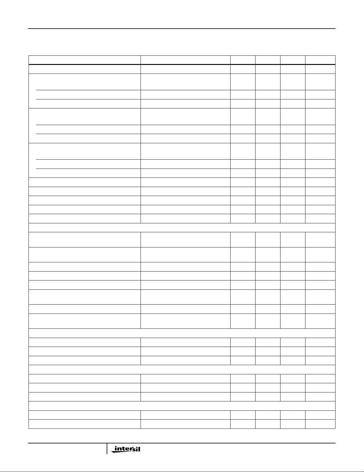
PARAMETER TEST CONDITIONS MIN TYP MAX UNITS
ACCURACY
Resolution 10 - - Bits
Integral Linearity Error, INL f
Differential Linearity Error, DNL
= 1MHz Sinewave - ±0.75 ±1.75 LSB
IN
= 1MHz Sinewave - ±0.35 ±1.0 LSB
f
IN
(Guaranteed No Missing Codes)
Offset Error, V
OS
Full Scale Error, FSE f
fIN = DC -40 - 40 LSB
= DC - 4 - LSB
IN
DYNAMIC CHARACTERISTICS
Minimum Conversion Rate No Missing Codes - 0.5 1 MSPS
Maximum Conversion Rate
HI5767/2 No Missing Codes 20 - - MSPS
HI5767/4 No Missing Codes 40 - - MSPS
HI5767/6 No Missing Codes 60 - - MSPS
Effective Number of Bits, ENOB
HI5767/2 fS = 20MSPS, fIN = 10MHz 8.7 9 - Bits
HI5767/4 f
HI5767/6 f
= 40MSPS, fIN = 10MHz 8.55 8.8 - Bits
S
= 60MSPS, fIN = 10MHz 8.1 8.4 - Bits
S
Signal to Noise and Distortion Ratio, SINAD
RMS Signal
--------------------------------------------------------------=
RMS Noise + Distortion
HI5767/2 f
HI5767/4 f
HI5767/6 f
= 20MSPS, fIN = 10MHz - 55.9 - dB
S
= 40MSPS, fIN = 10MHz - 54.7 - dB
S
= 60MSPS, fIN = 10MHz - 53.8 - dB
S
Signal to Noise Ratio, SNR
RMS Signal
-------------------------------=
RMS Noise
HI5767/2 f
HI5767/4 f
HI5767/6 f
= 20MSPS, fIN = 10MHz - 55.9 - dB
S
= 40MSPS, fIN = 10MHz - 55 - dB
S
= 60MSPS, fIN = 10MHz - 54 - dB
S
Total Harmonic Distortion, THD
HI5767/2 f
HI5767/4 f
= 20MSPS, fIN = 10MHz - -71 - dBc
S
= 40MSPS, fIN = 10MHz - -65 - dBc
S
4
Page 5
HI5767
Electrical Specifications AV
CC
= DV
= 5.0V, DV
CC1
CC2
= 3.0V; V
REFIN
= V
; fS = 40MSPS at 50% Duty Cycle;
REFOUT
CL= 10pF; TA = 25oC; Differential Analog Input; Typical Values are Test Results at 25oC,
Unless Otherwise Specified (Continued)
PARAMETER TEST CONDITIONS MIN TYP MAX UNITS
HI5767/6 fS = 60MSPS, fIN = 10MHz - -64.5 - dBc
2nd Harmonic Distortion
HI5767/2 f
HI5767/4 f
HI5767/6 f
= 20MSPS, fIN = 10MHz - -76 - dBc
S
= 40MSPS, fIN = 10MHz - -73 - dBc
S
= 60MSPS, fIN = 10MHz - -70 - dBc
S
3rd Harmonic Distortion
HI5767/2 f
HI5767/4 f
HI5767/6 f
= 20MSPS, fIN = 10MHz - -80 - dBc
S
= 40MSPS, fIN = 10MHz - -69 - dBc
S
= 60MSPS, fIN = 10MHz - -67 - dBc
S
Spurious Free Dynamic Range, SFDR
HI5767/2 f
HI5767/4 f
HI5767/6 f
Intermodulation Distortion, IMD f
Differential Gain Error f
Differential Phase Error f
= 20MSPS, fIN = 10MHz - 76 - dBc
S
= 40MSPS, fIN = 10MHz - 69 - dBc
S
= 60MSPS, fIN = 10MHz - 67 - dBc
S
= 1MHz, f2 = 1.02MHz - 64 - dBc
1
= 17.72MHz, 6 Step, Mod Ramp - 0.5 - %
S
= 17.72MHz, 6 Step, Mod Ramp - 0.2 - Degree
S
Transient Response (Note 2) - 1 - Cycle
Over-Voltage Recovery 0.2V Overdrive (Note 2) - 1 - Cycle
ANALOG INPUT
Maximum Peak-to-Peak Differential Analog Input
Range (V
+ - VIN-)
IN
Maximum Peak-to-Peak Single-Ended
- ±0.5 - V
- 1.0 - V
Analog Input Range
Analog Input Resistance, R
Analog Input Capacitance, C
Analog Input Bias Current, I
IN
IN
+ or IB- (Note 3) -10 - +10 µA
B
Differential Analog Input Bias Current
= (IB+- IB-)
I
BDIFF
(Note 3) - 1 - MΩ
-10- pF
(Note 3) - ±0.5 - µA
Full Power Input Bandwidth, FPBW - 250 - MHz
Analog Input Common Mode Voltage Range
Differential Mode (Note 2) 0.25 - 4.75 V
(VIN++ VIN-) / 2
INTERNAL REFERENCE VOLTAGE
Reference Voltage Output, V
Reference Output Current, I
REFOUT
(Loaded) - 2.5 - V
REFOUT
-12mA
Reference Temperature Coefficient - 120 - ppm/
REFERENCE VOLTAGE INPUT
Reference Voltage Input, V
REFIN
Total Reference Resistance, R
Reference Input Current, I
REFIN
REFIN
- 2.5 - V
- 2.5 - kΩ
-1-mA
DC BIAS VOLTAGE
DC Bias Voltage Output, V
DC
- 3.0 - V
Maximum Output Current - - 0.2 mA
o
C
5
Page 6
HI5767
Electrical Specifications AV
CC
= DV
= 5.0V, DV
CC1
CC2
= 3.0V; V
REFIN
= V
; fS = 40MSPS at 50% Duty Cycle;
REFOUT
CL= 10pF; TA = 25oC; Differential Analog Input; Typical Values are Test Results at 25oC,
Unless Otherwise Specified (Continued)
PARAMETER TEST CONDITIONS MIN TYP MAX UNITS
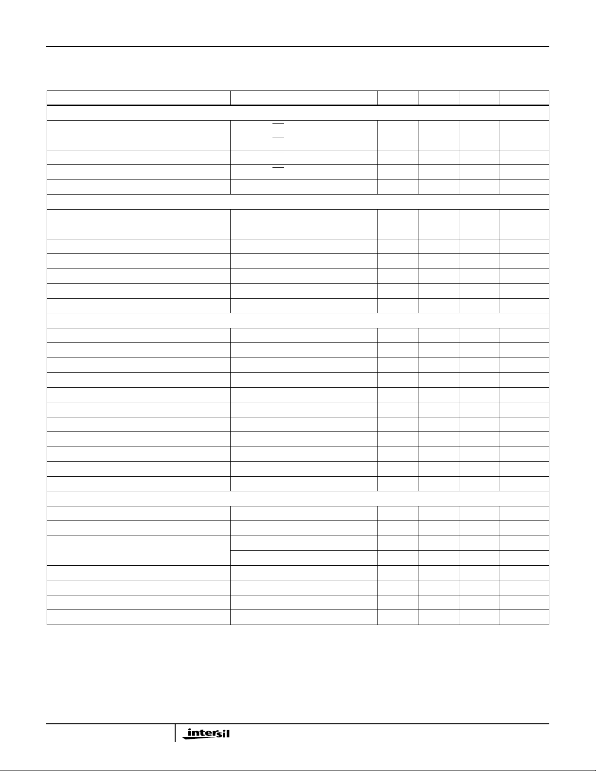
DIGITAL INPUTS
Input Logic High Voltage, V
Input Logic Low Voltage, V
Input Logic High Current, I
Input Logic Low Current, I
Input Capacitance, C
IN
IH
IL
IH
IL
CLK, DFS, OE 2.0 - - V
CLK, DFS, OE - - 0.8 V
CLK, DFS, OE, VIH= 5V -10.0 - +10.0 µA
CLK, DFS, OE, VIL= 0V -10.0 - +10.0 µA
-7- pF
DIGITAL OUTPUTS
Output Logic High Voltage, V
Output Logic Low Voltage, V
OH
OL
Output Three-State Leakage Current, I
Output Logic High Voltage, V
Output Logic Low Voltage, V
OH
OL
Output Three-State Leakage Current, I
Output Capacitance, C
OUT
OZ
OZ
IOH= 100µA; DV
IOL= 100µA; DV
VO = 0/5V; DV
IOH= 100µA; DV
IOL= 100µA; DV
VO = 0/5V; DV
= 5V 4.0 - - V
CC2
= 5V - - 0.8 V
CC2
= 5V -10 ±110 µA
CC2
= 3V 2.4 - - V
CC2
= 3V - - 0.5 V
CC2
= 3V -10 ±110 µA
CC2
-10- pF
TIMING CHARACTERISTICS
Aperture Delay, t
Aperture Jitter, t
Data Output Hold, t
Data Output Delay, t
AP
AJ
H
OD
Data Output Enable Time, t
Data Output Enable Time, t
Data Latency, t
LAT
EN
DIS
For a Valid Sample (Note 2) - - 7 Cycles
-5- ns
-5-ps
RMS
-5- ns
-6- ns
-5- ns
-5- ns
Power-Up Initialization Data Invalid Time (Note 2) - - 20 Cycles
Sample Clock Pulse Width (Low) f
Sample Clock Pulse Width (High) f
Sample Clock Duty Cycle Variation f
= 40MSPS 11.3 12.5 - ns
S
= 40MSPS 11.3 12.5 - ns
S
= 40MSPS - ±5- %
S
POWER SUPPLY CHARACTERISTICS
Analog Supply Voltage, AV
Digital Supply Voltage, DV
CC
CC1
Digital Output Supply Voltage, DV
CC2
At 3.0V 2.7 3.0 3.3 V
4.75 5.0 5.25 V
4.75 5.0 5.25 V
At 5.0V 4.75 5.0 5.25 V
Supply Current, I
CC
Power Dissipation f
Offset Error Sensitivity, ∆V
OS
Gain Error Sensitivity, ∆FSE AV
fIN = 1MHz and DFS = “0” - 62 - mA
= 1MHz and DFS = “0” - 310 - mW
IN
AVCCor DVCC = 5V ±5% - ±0.7 - LSB
or DVCC= 5V ±5% - ±0.1 - LSB
CC
NOTES:
2. Parameter guaranteed by design or characterization and not production tested.
3. With the clock low and DC input.
6
Page 7
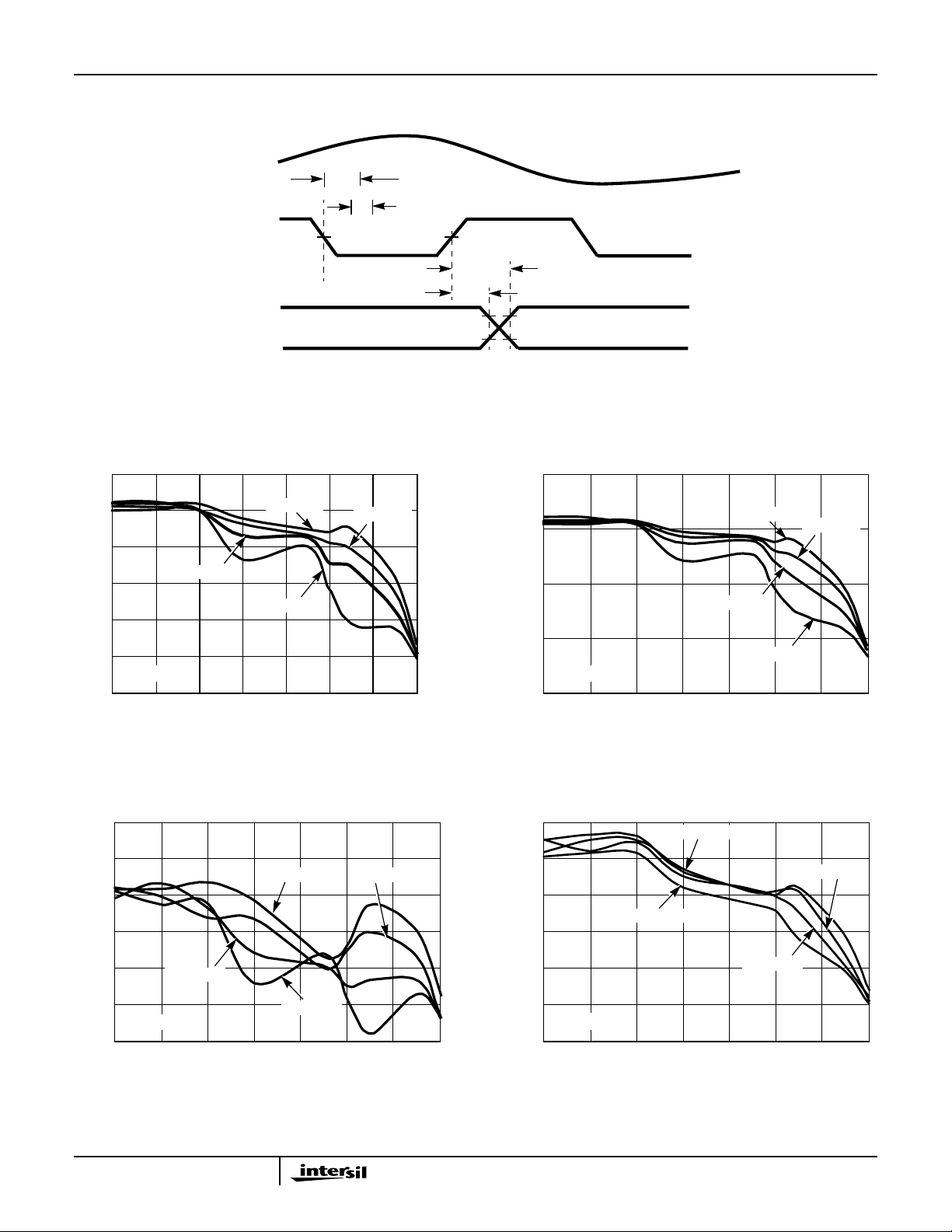
Timing Waveforms
ANALOG
INPUT
CLOCK
INPUT
DAT A
OUTPUT
1.5V
Typical Performance Curves
HI5767
t
AP
t
AJ
1.5V
t
OD
t
H
DATA N-1
FIGURE 1. INPUT TO OUTPUT TIMING
2.4V
0.5V
DATA N
9.5
9.0
8.5
8.0
ENOB (BITS)
7.5
7.0
TA = 25oC
6.5
10 20 30 40 50 60 70 80
fIN = 10MHz
SAMPLING FREQUENCY (MSPS)
fIN = 1MHz
fIN = 15MHz
fIN = 5MHz
FIGURE 2. EFFECTIVE NUMBER OFBITS (ENOB) AND
SINAD vs SAMPLING FREQUENCY
80
75
70
65
-THD (dBc)
60
fIN = 10MHz
fIN = 1MHz
fIN = 5MHz
59
53
47
41
SINAD (dB)
60
55
50
SNR (dB)
45
TA = 25oC
40
10 20 30 40 50 60 70 80
SAMPLING FREQUENCY (MSPS)
fIN = 1MHz
fIN = 10MHz
fIN = 15MHz
fIN = 5MHz
FIGURE 3. SNR vs SAMPLING FREQUENCY
80
75
70
65
SFDR (dBc)
60
fIN = 15MHz
fIN = 1MHz
fIN = 5MHz
fIN = 10MHz
55
TA = 25oC
50
10 20 30 40 50 60 70 80
SAMPLING FREQUENCY (MSPS)
fIN = 15MHz
55
TA = 25oC
50
10 20 30 40 50 60 70 80
SAMPLING FREQUENCY (MSPS)
FIGURE 4. -THD vs SAMPLING FREQUENCY FIGURE 5. SFDR vs SAMPLING FREQUENCY
7
Page 8
Typical Performance Curves (Continued)
HI5767
9.5
20MSPS
9.0
8.5
8.0
60MSPS
7.5
7.0
ENOB (BITS)
6.5
6.0
TA = 25oC, fIN = 10MHz
5.5
30 35 40 45 50 55 60 70
40MSPS
DUTY CYCLE (%, t
H/tCLK
)
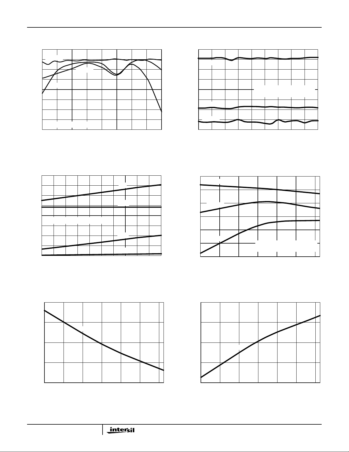
FIGURE 6. EFFECTIVE NUMBER OFBITS (ENOB) vs
SAMPLE CLOCK DUTY CYCLE
80
70
60
50
I
CC
AI
CC
9.1
9.0
20MSPS
8.9
8.8
8.7
8.6
ENOB (BITS)
40MSPS
8.5
60MSPS
8.4
65
8.3
0.25 0.75 1.25 1.75 2.25 2.75 3.25 4.75
TA = 25oC, fIN = 10MHz
DIFFERENTIAL ANALOG INPUT
3.75
4.25
VCM (V)
FIGURE 7. EFFECTIVE NUMBER OFBITS (ENOB) vs
ANALOG INPUT COMMON MODE VOLTAGE
9.2
20MSPS
9.0
8.8
40MSPS
40
TA = 25oC, 1MHz < fIN < 15MHz
30
20
SUPPLY CURRENT (mA)
10
0
10 15 20 25 30 35 40 55
fS (MSPS)
DI
CC1
DI
CC2
45
FIGURE 8. SUPPLY CURRENTvs SAMPLE CLOCK
FREQUENCY
2.530
) (V)
2.525
REFOUT
2.520
2.515
REFERENCE VOLTAGE, (V
2.510
-40 -20 0 20 40 80
V
REFOUT
TEMPERATURE (oC)
8.6
ENOB (BITS)
8.4
60MSPS
8.2
50
60
8.0
-40 -20 0 20 40 80
fIN = 10MHz, V
DIFFERENTIAL ANALOG INPUT
TEMPERATURE (oC)
REFIN
= V
60
REFOUT
FIGURE 9. EFFECTIVE NUMBER OFBITS (ENOB) vs
TEMPERATURE
3.1
(V)
3.0
DC
V
2.9
60
-40 -20 0 20 40 80
V
DC
TEMPERATURE (oC)
60
FIGURE 10. INTERNAL REFERENCE VOLTAGE (V
TEMPERATURE
8
REFOUT
)vs
FIGURE 11. DC BIAS VOLTAGE (VDC) vs TEMPERATURE
Page 9
Typical Performance Curves (Continued)
HI5767
6.5
6.0
t
OD
(ns)
5.5
OD
t
5.0
4.5
-40 -20 0 20 40 80
TEMPERATURE (oC)
60
80
I
70
CC
60
50
AI
CC
40
30
DI
CC1
20
SUPPLY CURRENT (mA)
10
DI
CC2
0
-40 -20 0 20 40 80
TEMPERATURE (oC)
60MSPS, fIN = 10MHz,
= DV
AV
CC
DV
CC2
60
CC1
=3V
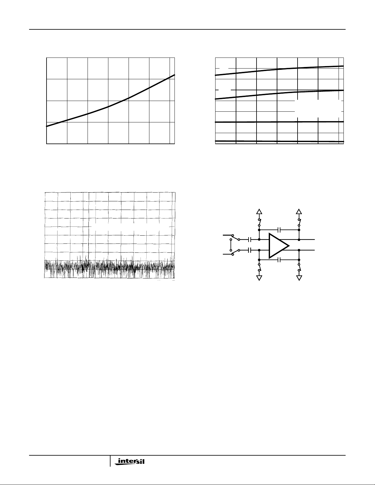
FIGURE 12. DATA OUTPUT DELAY (tOD) vs TEMPERATURE FIGURE 13. SUPPLY CURRENT vs TEMPERATURE
0
-10
-20
-30
-40
-50
-60
-70
OUTPUT LEVEL (dB)
-80
-90
-100
0 100 200 300 400 800600500 700 900 1023
TA = 25oC, fS = 60MSPS, fIN = 10MHz
FREQUENCY (BIN)
Φ
V
IN+
V
IN-
Φ
Φ
1
1
C
S
Φ
2
C
S
1
Φ
1
C
H
+
-
+
-
C
H
Φ
1
V
OUT+
V
OUT-
Φ
1
= 5V
FIGURE 14. 2048 POINT FFT PLOT FIGURE 15. ANALOG INPUT SAMPLE-AND-HOLD
9
Page 10
HI5767
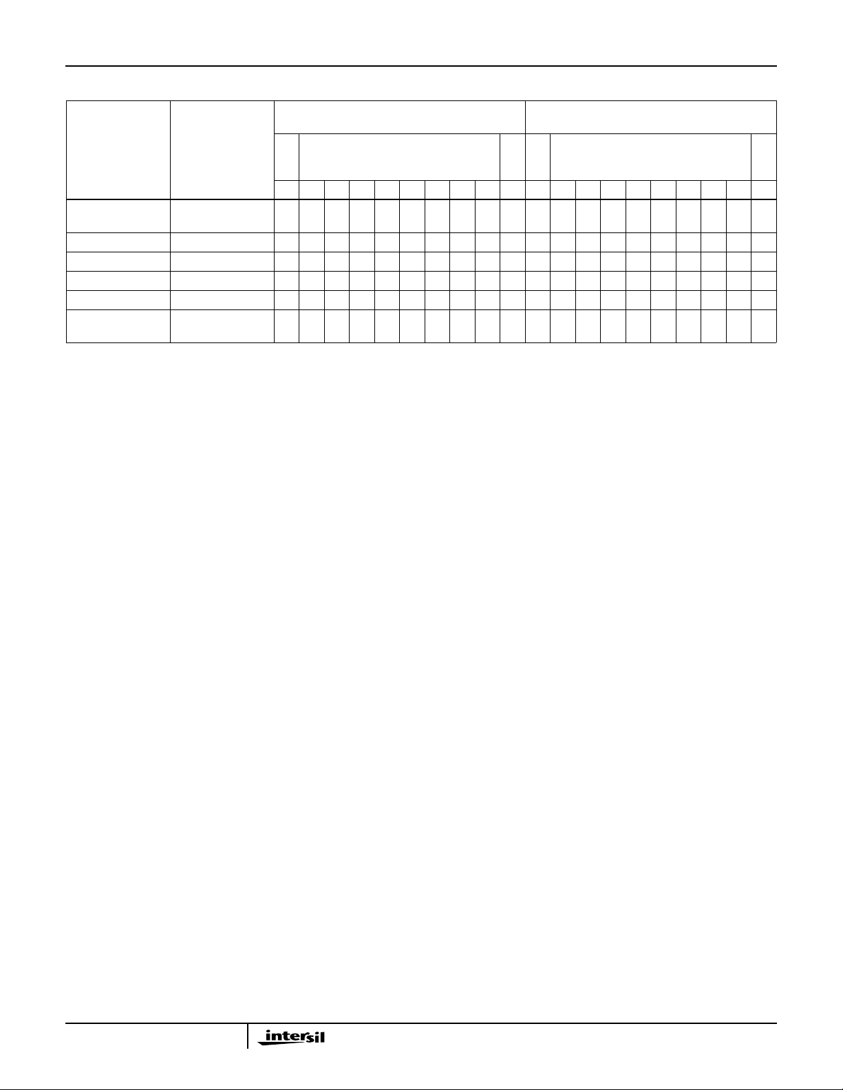
TABLE 1. A/D CODE TABLE
OFFSET BINARY OUTPUT CODE
(DFS LOW)
M
DIFFERENTIAL
CODE CENTER
DESCRIPTION
+Full Scale (+FS) -
1
/4 LSB
+FS - 11/4 LSB 0.498779V 1 1 1 11111100111111110
+3/4 LSB 732.422µV 10000000000000000000
-1/4 LSB -244.141µV 01111111111111111111
-FS + 13/4 LSB -0.498291V 0 0 0 00000011000000001
-Full Scale (-FS) +
3
/4 LSB
NOTE:
4. The voltages listed above represent the ideal center of each output code shown with V
INPUT VOLTAGE
(VIN+ - VIN-)
0.499756V 1 1 1 11111110111111111
-0.499268V 0 0 0 00000001000000000
S
B
D9 D8 D7 D6 D5 D4 D3 D2 D1 D0 D9 D8 D7 D6 D5 D4 D3 D2 D1 D0
B
REFIN
TWO’S COMPLEMENT OUTPUT CODE
(DFS HIGH)
L
M
S
S
B
= +2.5V.
L
S
B
Detailed Description
Theory of Operation
The HI5767 is a 10-bit fully differential sampling pipeline A/D
converter with digital error correction logic. Figure 16 depicts
the circuit for the front end differential-in-diff erential-out sampleand-hold (S/H). The switches are controlled by an internal
samplingclock which isa non-overlappingtwo phasesignal,Φ
and Φ2, derived from the master sampling clock. During the
sampling phase,Φ
capacitors, C
are discharged to analog ground. At the falling edge of Φ
input signal is sampled on the bottom plates of the sampling
capacitors. In the next clock phase , Φ
of the sampling capacitors are connected together and the
holding capacitors are switched to the op-amp output nodes.
The charge then redistributes between C
one sample-and-hold cycle. The front end sample-and-hold
output is a fully-differential, sampled-data representation of the
analog input. Thecircuit not onlyperformsthe sample-and-hold
function but will also convert a single-ended input to a fullydifferential output for the con v erter core. During the sampling
phase, the V
C
. The relatively small valuesof these components result in a
S
typical full power input bandwidth of 250MHz for the con v erter.
As illustrated in the functional block diagram and the timing
diagram in Figure 1, eight identical pipeline subconverter
stages, each containing a two-bit flash converter and a twobit multiplying digital-to-analog converter, follow the S/H
circuit with the ninth stage being a two bit flash converter.
Each converter stage in the pipeline will be sampling in one
phase and amplifying in the other clock phase. Each
individual subconverter clocksignal is offset by 180 degrees
from the previous stage clock signal resulting in alternate
stages in the pipeline performing the same operation.
, theinput signalis applied to the sampling
1
. At the same time the holding capacitors, CH,
S
, the two bottom plates
2
and CH completing
S
pins see only the on-resistance of a switch and
IN
1
the
The output of each of the eight identical two-bit subconverter
stages is a two-bitdigital wordcontaining a supplementary bit
to be used by the digital error correction logic. The output of
each subconverter stageis input toa digital delayline which is
controlled by the internal sampling clock. The function of the
digital dela yline is to time align the digital outputs of the eight
identical two-bit subconverter stages with the corresponding
1
output of the ninth stage flash converter before applying the
eighteen bit result to the digital error correction logic. The
digital error correction logic uses the supplementary bits to
correct any error that may exist beforegenerating the final ten
bit digital data output of the converter.
Because of the pipeline nature of this converter, the digital data
representing an analoginputsample isoutput tothe digital data
bus on the 7th cycle of the clock after the analog sample is
taken. This time delay is specified as the data latency. After the
data latency time, the digital data representing each
succeeding analog sample is output during the following clock
cycle. The digital output data is synchronized to the external
sampling clock by a double b uff ered latching technique . The
digital output data is available in tw o’s complement or offset
binary f ormatdepending on thestate ofthe Data FormatSelect
(DFS) control input (see Table 1, A/D Code Table).
Internal Reference Voltage Output, V
REFOUT
The HI5767 is equipped with an internal reference voltage
generator,therefore,noexternal reference v oltageis required.
V
REFOUT
must be connected to V
when using the
REFIN
internal reference voltage.
An internal band-gap reference voltage followed by an
amplifier/buffer generates the precision +2.5V reference
voltage used by the converter. A 4:1 array of substrate
PNPs generates the “delta-V
” and a two-stage op-amp
BE
closes the loop to create an internal +1.25V band-gap
reference voltage. This voltage is then amplified by a
wideband uncompensated operational amplifier connected
10
Page 11
HI5767
in a gain-of-two configuration. An external, user-supplied,
0.1µF capacitorconnected fromthe V
REFOUT
output pin to
analog ground is used to set the dominant pole and to
maintain the stability of the operational amplifier.
Reference Voltage Input, V
REFIN
The HI5767 is designed to accept a +2.5V reference voltage
source at the V
converter requires V
tested with V
REFIN
input pin. Typical operation of the
REFIN
to be set at +2.5V. The HI5767 is
REFIN
connected to V
REFOUT
yielding a fully
differential analog input voltage range of±0.5V.
The user does have the option of supplying an external
+2.5V reference voltage. As a result of the high input
impedance presented at the V
input pin, 2.5kΩ
REFIN
typically, the external reference voltage being used is only
required to source 1mA of reference input current. In the
situation where an external reference voltage will be used
an external 0.1µF capacitor must be connected from the
V
REFOUT
output pin to analog ground in order to maintain
the stability of the internal operational amplifier.
In order to minimize overall converter noise it is
recommended that adequate high frequency decoupling be
provided at the reference voltage input pin, V
REFIN
.
Analog Input, Differential Connection
The analog input tothe HI5767 is a differential inputthat can
be configured in various ways depending on the signal
source and the required level of performance. A fully
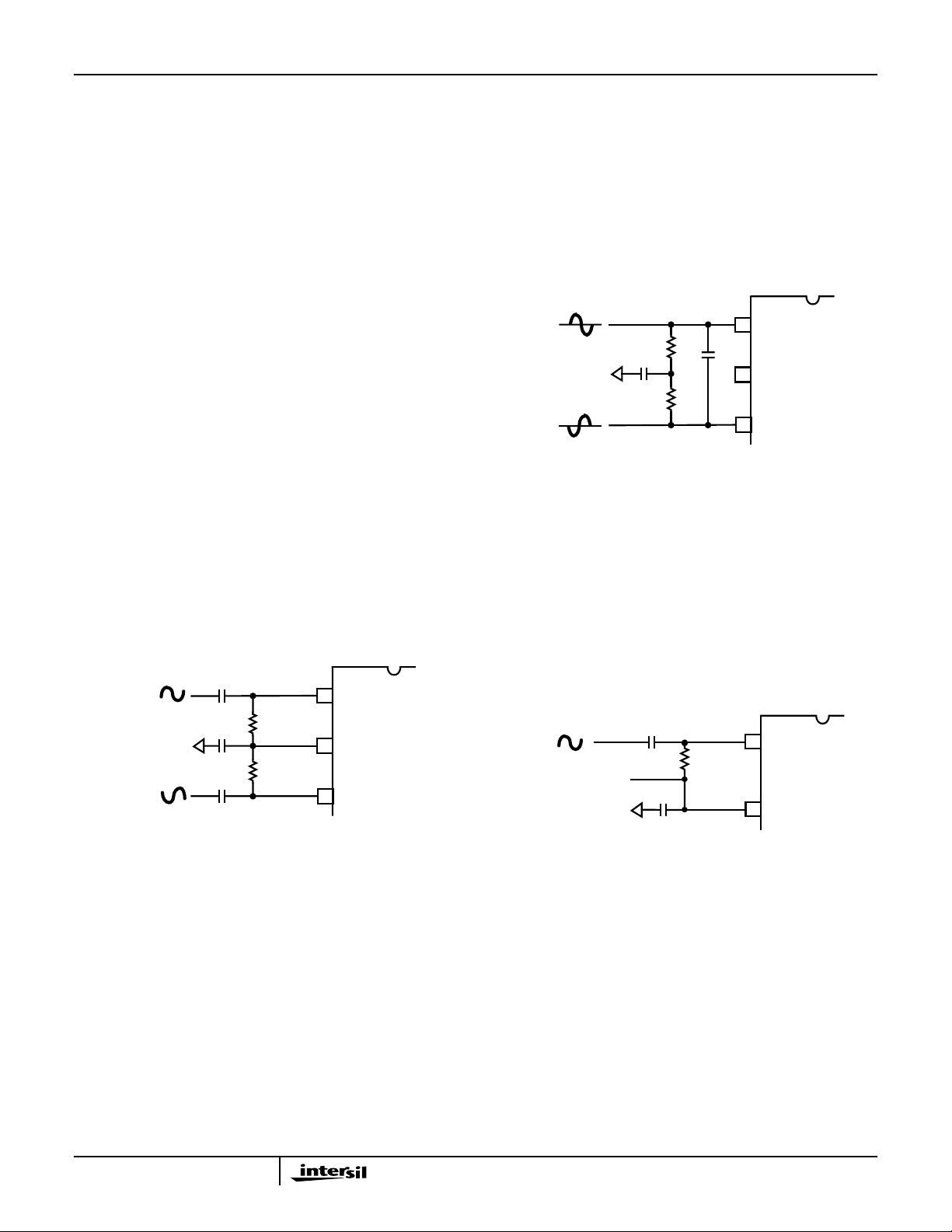
differential connection (Figure 17 and Figure 18) will deliver
the best performance from the converter.
V
IN
VIN+
and -VIN input signals are 0.5V
the V
IN
180 degrees out of phase with V
positive full scale when the V
the V
- input is at VDC- 0.25V (VIN+-VIN- = +0.5V).
IN
. The converter will be at
IN
+ input is at VDC+ 0.25V and
IN
, with -VIN being
P-P
Conversely, the converter will be at negative full scale when
the V
+ input is equal to VDC- 0.25V and VIN- is at
IN
V
+ 0.25V (VIN+-VIN- = -0.5V).
DC
The analog input can be DC coupled (Figure 18) as long as
the inputs are withinthe analog input common mode voltage
range (0.25V ≤ VDC ≤ 4.75V).
V
IN
VDC
R
-V
IN
VDC
FIGURE 17. DC COUPLED DIFFERENTIAL INPUT
R
VIN+
V
DC
VIN-
HI5767
C
The resistors, R, in Figure 18 are not absolutely necessary
but may be used as load setting resistors. A capacitor, C,
connected from V
+ to VIN- will help filter any high
IN
frequency noise on the inputs, also improving performance.
Values around 20pF are sufficient and can be used on AC
coupled inputs as well. Note, however, that the value of
capacitor C chosen must take into account the highest
frequency component of the analog input signal.
Analog Input, Single-Ended Connection
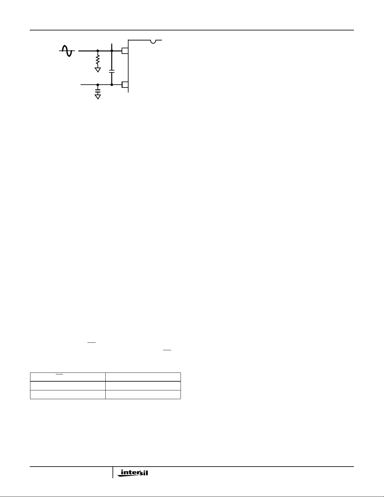
The configuration shown in Figure 19 may be used with a
single ended AC coupled input.
R
R
-V
IN
FIGURE 16. AC COUPLED DIFFERENTIAL INPUT
V
DC
VIN-
HI5767
Since the HI5767 is poweredby a single +5V analog supply,
the analog input is limited to be between ground and +5V.
For the differential input connection this implies the analog
input commonmode voltagecan range from 0.25V to4.75V.
The performance of the ADC does not change significantly
with the value of the analog input common mode voltage.
A DC voltage source, V
, equal to 3.2V (typical), is made
DC
availableto theuser tohelp simplify circuit design when using
an AC coupled differential input. This lo w output impedance
voltagesource is notdesigned to bea reference butmakes an
excellent DC bias source and stays well within the analog
input common mode voltage range ov er temper ature .
For the AC coupled differential input (Figure 17) and with
V
connected to V
REFIN
REFOUT
, full scale is achieved when
11
V
IN
R
VDC
FIGURE 18. AC COUPLED SINGLE ENDED INPUT
Again, with V
sinewav e, then VIN+ is a 1.0V
connected to V
REFIN
REFOUT
sinewav e riding on a positive
P-P
VIN+
HI5767
VIN-
, if VIN is a 1V
P-P
voltage equal to VDC. The converter will be at positive full scale
when V
negativefull scale whenV
+ is at VDC + 0.5V (VIN+-VIN- = +0.5V) and will be at
IN
+ is equalto VDC - 0.5V (VIN+-VIN-
IN
= -0.5V). Sufficient headroom must be provided such that the
input voltage nevergoes above +5V orbelowAGND .In thiscase,
VDC could range between 0.5V and 4.5V without a significant
change in ADC performance. The simplest wa y to produce VDC
is to use the DC bias source, V
, output of the HI5767.
DC
The single ended analog input can be DC coupled
(Figure 20) as long as the input is within the analog input
common mode voltage range.
Page 12
HI5767
V
IN
V
DC
R
V
DC
FIGURE 19. DC COUPLED SINGLE ENDED INPUT
VIN+
C
HI5767
VIN-
The resistor, R, in Figure 20 is not absolutely necessary but
may be used as a load setting resistor. A capacitor, C,
connected from V
+ to VIN- will help filter any high
IN
frequency noise on the inputs, also improving performance.
Values around 20pF are sufficient and can be used on AC
coupled inputs as well. Note, however, that the value of
capacitor C chosen must take into account the highest
frequency component of the analog input signal.
A single ended source may give better overall system
performance if it is first converted to differential before
driving the HI5767.
Digital Output Control and Clock Requirements
The HI5767 provides a standard high-speed interface to
external TTL logic families.
In order to ensurerated performance of the HI5767, theduty
cycle of the clock should be held at 50% ±5%. It must also
have low jitter and operate at standard TTL levels.
Performance of the HI5767 will only be guaranteed at
conversion rates above 1 MSPS. This ensures proper
performance ofthe internal dynamiccircuits. Similarly, when
power is first applied to the converter, a maximum of 20
cycles at a sample rate above 1 MSPS will have to be
performed before valid data is available.A Data Format
Select (DFS) pin is provided which will determine the format
of thedigital data outputs. When at logic low, the data will be
output in offset binary format. When at logic high, the data
will be output in two’s complement format. Refer to Table 1
for further information.
The output enable pin,
the digital outputs to a high impedance state. Set the
input to logic low for normal operation.
OE, when pulled high will three-state
OE
The part shouldbe mountedon aboard thatprovides separate
low impedance connections for the analog and digital supplies
and grounds. Forbest performance, the supplies to the HI5767
should be driven by clean, linear regulatedsupplies. Theboard
should also have good high frequency decoupling capacitors
mounted as close as possible to the converter . If the part is
powered off a single supply, then the analog supply should be
isolated with a ferrite bead from the digital supply.
Refer to the application note “Using Intersil High Speed A/D
Converters” (AN9214) for additional considerations when
using high speed converters.
Static Performance Definitions
Offset Error (VOS)
The midscalecode transition should occur at a level1/4LSB
above half-scale. Offset is defined as the deviation of the
actual code transition from this point.
Full-Scale Error (FSE)
The last code transition should occur foran analoginput that
3
is
/4 LSB below Positive Full Scale (+FS) with the offset
error removed. Full scale error is defined as the deviation of
the actual code transition from this point.
Differential Linearity Error (DNL)
DNL is the worst case deviation of a code width from the
ideal value of 1 LSB.
Integral Linearity Error (INL)
INL is the worst case deviation of a code center from a best
fit straight line calculated from the measured data.
Power Supply Sensitivity
Each ofthe powersupplies aremoved plus and minus5% and
the shift in the offset and full scale error (in LSBs) is noted.
Dynamic Performance Definitions
FastFourier Transform (FFT) techniques are used toevaluate
the dynamic performance of the HI5767. A low distortion sine
wave is applied to the input, it is coherently sampled, and the
output is stored in RAM. Thedata isthen transformed into the
frequency domain with an FFT and analyzed to evaluate the
dynamic performance of the A/D . The sine w ave input to the
part is typically -0.5dB down from full scale for all these tests.
OE INPUT DIGITAL DATA OUTPUTS
0 Active
1 High Impedance
Supply and Ground Considerations
The HI5767 has separate analog and digital supply and
ground pins to keep digital noise out of the analog signal
path. The digital data outputs also have a separate supply
pin, DV
supply. This allows the outputs to interface with3.0V logicif
so desired.
, which can be powered from a 3.0V or 5.0V
CC2
12
SNR and SINAD are quoted in dB. The distortion numbers are
quoted in dBc (decibels with respect to carrier) and DO NO T
include any correction factors f or normalizing to full scale.
The Effective Number of Bits (ENOB) is calculated from the
SINAD data by:
ENOB = (SINAD - 1.76 + V
where: V
V
adjusts the SINAD, and hence the ENOB, for the
CORR
= 0.5 dB (Typical).
CORR
CORR
) / 6.02,
amount the analog input signal is backed off from full scale.
Page 13

HI5767
Signal To Noise and Distortion Ratio (SINAD)
SINAD isthe ratio of the measuredRMS signal to RMS sum
of all the other spectral components below the Nyquist
frequency, f
/2, excluding DC.
S
Signal To Noise Ratio (SNR)
SNR is the ratio of the measured RMS signal to RMSnoise at
a specified input and sampling frequency. The noise is the
RMS sum of all of the spectral components below f
excluding the fundamental, the first five harmonics and DC.
/2
S
Total Harmonic Distortion (THD)
THD is the ratio of the RMS sum of the first 5 harmonic
components to the RMS value of the fundamental input signal.
2nd and 3rd Harmonic Distortion
This is the ratio of the RMS value of the applicable harmonic
component to the RMS value of the fundamental input signal.
Spurious Free Dynamic Range (SFDR)
SFDR is the ratio of the fundamental RMS amplitude to the
RMS amplitude of the next largest spectral component in the
spectrum below f
/2.
S
Intermodulation Distortion (IMD)
Nonlinearities in the signal path will tend to generate
intermodulation products when two tones, f
present at the inputs.The ratioof themeasured signalto the
distortion terms is calculated. The terms included in the
calculation are (f
(f
+2f2), (f1-2f2). The ADC is tested with each tone 6dB
1
below full scale.
), (f1-f2), (2f1), (2f2), (2f1+f2), (2f1-f2),
1+f2
and f2, are
1
Transient Response
Transient response is measured by providing a full-scale
transition to the analog input of the ADC and measuring the
number of cycles it takes for the output code to settle within
10-bit accuracy.
Over-Voltage Recovery
Over-Voltage Recoveryis measuredby providing a full-scale
transition to the analog input of the ADC which overdrives
the input by 200mV, and measuring the number of cycles it
takes for the output code to settle within 10-bit accuracy.
Full Power Input Bandwidth (FPBW)
Full power input bandwidth is the analog input frequency at
which the amplitude of the digitally reconstructed output has
decreased 3dB below the amplitude of the input sine wave.
The input sine wave has an amplitude which swings from
-FS to +FS. The bandwidth given is measured at the
specified sampling frequency.
Video Definitions
Differential Gain and Differential Phase are two commonly
found video specifications forcharacterizing the distortion of
a chrominance signal as itis offset through the input voltage
range of an ADC.
Differential Gain (DG)
Differential Gain is the peak difference in chrominance
amplitude (in percent) relative to the reference burst.
Differential Phase (DP)
Differential Phase is the peak difference in chrominance
phase (in degrees) relative to the reference burst.
Timing Definitions
Refer to Figure 1 and Figure 2 for these definitions.
Aperture Delay (tAP)
Aperture delay is the time delay between the external
sample command (the falling edgeof theclock) andthe time
at which the signal is actually sampled. This delay is due to
internal clock path propagation delays.
Aperture Jitter (tAJ)
Aperture jitter is the RMS variation in the aperture delay due
to variation of internal clock path delays.
Data Hold Time (tH)
Data hold time is the time to where the previous data (N - 1)
is no longer valid.
Data Output Delay Time (tOD)
Data output delay time is the timeto where the new data (N)
is valid.
Data Latency (t
After the analogsample is taken, the digitaldata representing
an analog input sample is output to the digital data bus on
the 7th cycle of the clock after the analog sample is taken.
This is due to the pipeline nature of the converter where the
analog sample has to ripple throughthe internal subconverter
stages. This delay is specified as the data latency. After the
data latency time, the digital data representing each
succeeding analog sample is output during the following
clock cycle. Thedigital datalags the analoginput sample by7
sample clock cycles.
Power-Up Initialization
This timeis defined as the maximumnumber of clock cycles
that are required to initialize the converter at power-up. The
requirement arises from the need to initialize the dynamic
circuits within the converter.
LAT
)
All Intersil semiconductor products are manufactured, assembled and tested under ISO9000 quality systems certification.
Intersil semiconductor products are sold by description only.Intersil Corporation reserves the right to make changes in circuit design and/or specifications at any time without notice. Accordingly, the reader is cautioned to verify that data sheets are current before placing orders. Information furnished by Intersil is believed to be accurate and
reliable. However ,no responsibility is assumed by Intersil or its subsidiaries for its use; nor for any infringements of patents or other rights of third parties which may result
from its use. No license is granted by implication or otherwise under any patent or patent rights of Intersil or its subsidiaries.
For information regarding Intersil Corporation and its products, see web site www.intersil.com
13
 Loading...