


HI5800
Data Sheet June 1999
12-Bit, 3MSPS, Sampling A/D Converter
The HI5800 is a monolithic, 12-bit, sampling Analog-toDigital Converter fabricated in the HBC10 BiCMOS process.
It is a complete subsystem containing a sample and hold
amplifier, voltage reference, two-step subranging A/D, error
correction, control logic,andtiming generator. The HI5800 is
designed forhigh speed applications where wide bandwidth,
accuracy and low distortion are essential.
Ordering Information
TEMP.
PART
NUMBER LINEARITY
HI5800BID ±1 LSB -40 to 85 40 Ld SBDIP D40.6
HI5800JCD
HI5800KCD
±2 LSB
±1 LSB
HI5800-EV 25 Evaluation Board
RANGE
(oC) PACKAGE
PKG.
NO.
0 to 70 40 Ld SBDIP D40.6
File Number 2938.10
Features
• Throughput Rate . . . . . . . . . . . . . . . . . . . . . . . . . .3MSPS
• 12-Bit, No Missing Codes Over Temperature
• Integral Linearity Error . . . . . . . . . . . . . . . . . . . . . 1.0 LSB
• Buffered Sample and Hold Amplifier
• Precision Voltage Reference
• Input Signal Range. . . . . . . . . . . . . . . . . . . . . . . . . . ±2.5V
• 20MHz Input BW Allows Sampling Beyond Nyquist
• Zero Latency/No Pipeline Delay
Applications
• High Speed Data Acquisition Systems
• Medical Imaging
• Radar Signal Analysis
• Document and Film Scanners
• Vibration/Waveform Spectrum Analysis
• Digital Servo Control
Pinout
HI5800
(SBDIP)
TOP VIEW
REF
RO
RG
REF
ADJ
ADJ
AV
CC
OUT
V
AGND
ADJ+
ADJ-
AV
EE
AV
CC
AGND
AV
EE
A0
CS
OE
CONV
DV
EE
DGND
DV
CC
1
IN
2
3
4
5
6
IN
7
8
9
10
11
12
13
14
15
16
17
18
19
20
40
39
38
37
36
35
34
33
32
31
30
29
28
27
26
25
24
23
22
21
IRQ
OVF
AV
CC
D11 (MSB)
D10
D9
D8
DV
CC
DGND
AGND
AV
EE
D7
D6
D5
D4
D3
D2
D1
D0 (LSB)
AV
CC
1
CAUTION: These devices are sensitive to electrostatic discharge; follow proper IC Handling Procedures.
1-888-INTERSIL or 321-724-7143
| Copyright © Intersil Corporation 1999

Functional Block Diagram
REF
OUT
REF
IN
REFERENCE
HI5800
LATCH
7-BIT
D0 (LSB)
D1
D2
DIGITAL
OUTPUTS
ADJ+
ADJ-
V
IN
AV
S AND H
CCAVEEDVCCDVEE
Typical Application Schematic
+10µF
C23
0.1µF
C22
0.01µF
C1
V
IN
CONV
OE
A0
CS
7-BIT
FLASH
X32
AGND DGND
HI5800
(1)
REF_IN
REF_OUT
AGND
AGND
AGND
DGND
DGND
V
CONV
OE
A0
CS
(5)
(7)
(12)
(31)
(19)
(32)
(6)
IN
(37)
(17)
(16)
(14)
(15)
(22)
(MSB)D11
(18)
(33)
(20)
(LSB)
(23)
(24)
(25)
(26)
(27)
(28)
(29)
(34)
(35)
(36)
(40)
(39)
DV
DV
D0
D1
D2
D3
D4
D5
D6
D7
D8
D9
D10
IRQ
OVF
EE
CC
7-BIT
LATCH
7-BIT
DAC
D0
D1
D2
D3
D4
D5
D6
D7
D8
D9
D10
D11
IRQ
OVF
ADJ
10µF
OUTPUT LATCHES
CONTROL
LOGIC
AND
TIMING
0.1µF
+
10µF
ERROR CORRECTION
RG
10µF, 0.1µF, AND 0.01µF CAPS ARE PLACED
AS CLOSE TO PART AS POSSIBLE
0.1µF
ADJ
BNC
GND
RO
+
D10
D11 (MSB)
OVF
IRQ
CS
CONV
OE
AO
AV
AV
CC
R9
10K
EE
R11
10K
R10
10K
2
RO_ADJ
RG_ADJ
(8)
ADJ+
(9)
ADJ-
(2)
(3)
(4)
AV
(11)
AV
(21)
(38)
(10)
AV
(13) (30)
CC
CC
EE
0.1µF
10µF
+
0.1µF 10µF
+

HI5800
Absolute Maximum Ratings Thermal Information
Supply Voltages
AVCC or DVCC to GND . . . . . . . . . . . . . . . . . . . . . . . . . . . . +5.5V
AVEE or DVEE to GND. . . . . . . . . . . . . . . . . . . . . . . . . . . . . -5.5V
DGND to AGND . . . . . . . . . . . . . . . . . . . . . . . . . . . . . . . . . . ±0.3V
Analog Input Pins
Reference Input REFIN . . . . . . . . . . . . . . . . . . . . . . . . . . . +2.75V
Signal Input VIN . . . . . . . . . . . . . . . . . . . . . . . . . . ±(REFIN +0.2V)
RO
, RG
ADJ
Digital I/O Pins. . . . . . . . . . . . . . . . . . . . . . . . . . . . . . . .GND to V
, ADJ+, ADJ-. . . . . . . . . . . . . . . . . . . . . VEE to V
ADJ
CC
CC
Operating Conditions
Temperature Range
HI5800JCD/KCD . . . . . . . . . . . . . . . . . . . . . . . . . . . . 0oC to 70oC
HI5800BID . . . . . . . . . . . . . . . . . . . . . . . . . . . . . . . -40oC to 85oC
CAUTION: Stresses above those listed in “Absolute Maximum Ratings” may cause permanent damage to the device. This is a stress only rating and operation of the
device at these or any other conditions above those indicated in the operational sections of this specification is not implied.
NOTE:
1. θJA is measured with the component mounted on an evaluation PC board in free air.
Thermal Resistance (Typical, Note 1) θJA (oC/W) θJC (oC/W)
SBDIP Package . . . . . . . . . . . . . . . . . . 40 15
Maximum Junction Temperature
SBDIP Package . . . . . . . . . . . . . . . . . . . . . . . . . . . . . . . . . .175oC
Maximum Storage Temperature Range. . . . . . . . . . -65oC to 150oC
Maximum Lead Temperature (Soldering, 10s). . . . . . . . . . . . .300oC
Electrical Specifications AV
PARAMETER TEST CONDITIONS
SYSTEM PERFORMANCE
Resolution 12 - - 12 - - Bits
Integral Linearity Error, INL fS = 3MHz, fIN = 45Hz Ramp - 0.7 ±2-±0.5 ±1 LSB
Differential Linearity Error, DNL
(Guaranteed No Missing Codes)
Offset Error, V
(Adjustable to Zero)
Full Scale Error, FSE
(Adjustable to Zero)
DYNAMIC CHARACTERISTICS (Input Signal Level 0.5dB Below Full Scale)
Throughput Rate No Missing Codes 3.0 - - 3.0 - - MSPS
Signal to Noise Ratio (SNR) fS = 3MHz, fIN = 20kHz 66 69 - 68 71 - dB
RMS Signal
=
------------------------------RMS Noise
Signal to Noise Ratio (SINAD) f
--------------------------------------------------------------
=
RMS Noise + Distortion
Total Harmonic Distortion, THD f
Spurious Free Dynamic Range,
SFDR
Intermodulation Distortion, IMD fS = 3MHz, f1 = 49kHz,
Differential Gain fS = 1MHz - 0.9 - - 0.9 - %
Differential Phase fS = 1MHz - 0.05 - - 0.05 - Degrees
Aperture Delay, t
OS
RMS Signal
AD
= +5V, DVCC = +5V, AVEE = -5V, DVEE = -5V; Internal Reference Used,
CC
Unless Otherwise Specified
HI5800JCD HI5800KCD, HI5800BID
0oC TO 70oC
0oC TO 70oC
MIN TYP MAX MIN TYP MAX
fS = 3MHz, fIN = 45Hz Ramp - ±0.5 ±1-±0.3 ±1 LSB
(Note 8) JCD, KCD - ±2 ±15 - ±2 ±15 LSB
BID - - - - ±3 ±15 LSB
(Note 8) JCD, KCD - ±2 ±15 - ±2 ±10 LSB
BID - - - - ±3 ±15 LSB
fS = 3MHz, fIN = 1MHz 65 67 - 67 69 - dB
= 3MHz, fIN = 20kHz 66 68 - 68 71 - dB
S
fS = 3MHz, fIN = 1MHz 65 67 - 67 68 - dB
= 3MHz, fIN = 20kHz - -74 -70 - -85 -74 dBc
S
fS = 3MHz, fIN = 1MHz - -70 -68 - -77 -70 dBc
fS = 3MHz, fIN = 20kHz 71 76 - 76 86 - dBc
fS = 3MHz, fIN = 1MHz 68 72 - 71 77 - dBc
- -74 -66 - -79 -70 dBc
f2 = 50kHz (Note 3)
(Note 3) - 12 20 - 12 20 ns
-40oC TO 85oC
UNITS
3

HI5800
Electrical Specifications AV
= +5V, DVCC = +5V, AVEE = -5V, DVEE = -5V; Internal Reference Used,
CC
Unless Otherwise Specified (Continued)
HI5800JCD HI5800KCD, HI5800BID
0oC TO 70oC
PARAMETER TEST CONDITIONS
Aperture Jitter, t
AJ
0oC TO 70oC
MIN TYP MAX MIN TYP MAX
(Note 3) - 10 20 - 10 20 ps
-40oC TO 85oC
UNITS
ANALOG INPUT
Input Voltage Range - ±2.5 ±2.7 - ±2.5 ±2.7 V
Input Resistance 1 3 - 1 3 - MΩ
Input Capacitance - 5 - - 5 - pF
Input Current - ±1 ±10 - ±1 ±10 µA
Input Bandwidth - 20 - - 20 - MHz
INTERNAL VOLTAGE REFERENCE
Reference Output Voltage,
REF
OUT
(Loaded)
2.450 2.500 2.550 2.470 2.500 2.530 V
Reference Output Current (Note 5) 2 - - 2 - - mA
Reference Temperature
-20- -13-ppm/
Coefficient
REFERENCE INPUT
Reference Input Range - 2.5 2.6 - 2.5 2.6 V
Reference Input Resistance - 200 - - 200 - Ω
DIGITAL INPUTS
Input Logic High Voltage, V
Input Logic Low Voltage, V
Input Logic Current, I
IL
Digital Input Capacitance, C
IH
IL
IN
(Note 6) 2.0 - - 2.0 - - V
- - 0.8 - - 0.8 V
VIN = 0V, 5V - ±1 ±10 - ±1 ±10 µA
VIN = 0V - 5 - - 5 - pF
DIGITAL OUTPUTS
Output Logic High Voltage, V
Output Logic Low Voltage, V
Output Logic High Current, I
Output Logic Low Current, I
Output Three-State Leakage
Current, I
OZ
Digital Output Capacitance, C
OH
OL
OH
OL
OUT
I
= -160µA 2.4 4.3 - 2.4 4.3 - V
OUT
I
= 3.2mA - 0.22 0.4 - 0.22 0.4 V
OUT
-0.160 -6 - -0.160 -6 - mA
3.2 6 - 3.2 6 - mA
V
= 0V, 5V - ±1 ±10 - ±1 ±10 µA
OUT
-10- -10-pF
TIMING CHARACTERISTICS
Minimum CONV Pulse, t
CS to CONV Setup Time, t
CONV to CS Setup Time, t
Minimum OE Pulse, t
CS to OE Setup Time, t
OE to CS Setup Time, t
1
2
3
4
5
6
IRQ Delay from Start Convert, t
IRQ Pulse Width, t
8
(Notes 3, 4) 10 - - 10 - - ns
(Note 3) 10 - - 10 - - ns
(Note 3) 0 - - 0 - - ns
(Notes 3, 5) 15 - - 15 - - ns
(Note 3) 0 - - 0 - - ns
(Note 3) 0 - - 0 - - ns
(Note 3) 10 20 25 10 20 25 ns
7
JCD, KCD 190 200 230 190 200 230 ns
BID - - - 180 195 230 ns
Minimum Cycle Time for
Conversion, t
9
IRQ to Data Valid Delay, t
Minimum A0 Pulse, t
11
10
(Note 3) -5 0 +5 -5 0 +5 ns
(Notes 3, 5) 10 - - 10 - - ns
- 325 333 - 325 333 ns
o
C
4
HI5800
Electrical Specifications AV
= +5V, DVCC = +5V, AVEE = -5V, DVEE = -5V; Internal Reference Used,
CC
Unless Otherwise Specified (Continued)
HI5800JCD HI5800KCD, HI5800BID
0oC TO 70oC
PARAMETER TEST CONDITIONS
Data Access from OE Low, t
12
0oC TO 70oC
MIN TYP MAX MIN TYP MAX
(Note 3) 10 18 25 10 18 25 ns
-40oC TO 85oC
UNITS
LSB, Nibble Delay from A0 High, t13(Note 3) - 10 20 - 10 20 ns
MSB Delay from A0 Low, t
CS to Float Delay, t
Minimum CS Pulse, t
15
16
CS to Data Valid Delay, t
Output Fall 2 Time, t
Output Rise Time, t
f
r
14
17
(Note 3) - 14 20 - 14 20 ns
(Note 3) 10 18 25 10 18 25 ns
(Notes 3, 5) 15 - - 15 - - ns
(Note 3) 10 18 25 10 18 25 ns
(Note 3) - 5 20 - 5 20 ns
(Note 3) - 5 20 - 5 20 ns
POWER SUPPLY CHARACTERISTICS
IV
IV
IDV
IDV
CC
EE
CC
EE
- 170 220 - 170 220 mA
- 150 190 - 150 190 mA
- 24 40 - 24 40 mA
-25-25mA
Power Dissipation - 1.7 2.2 - 1.7 2.2 W
PSRR VCC, VEE±5% - 0.01 - - 0.01 - %/%
NOTES:
2. Dissipation rating assumes device is mounted with all leads soldered to printed circuit board.
3. Parameter guaranteed by design or characterization and not production tested.
4. Recommended pulse width for CONV is 60ns.
5. Recommended minimum pulse width is 25ns.
6. This is the additional current available from the REF
pin with the REF
OUT
pin driving the REFIN pin.
OUT
7. The A0 pin VIH at -40oC may exceed 2.0V by up to 0.4V at initial power up.
8. Excludes error due to internal reference temperature drift.
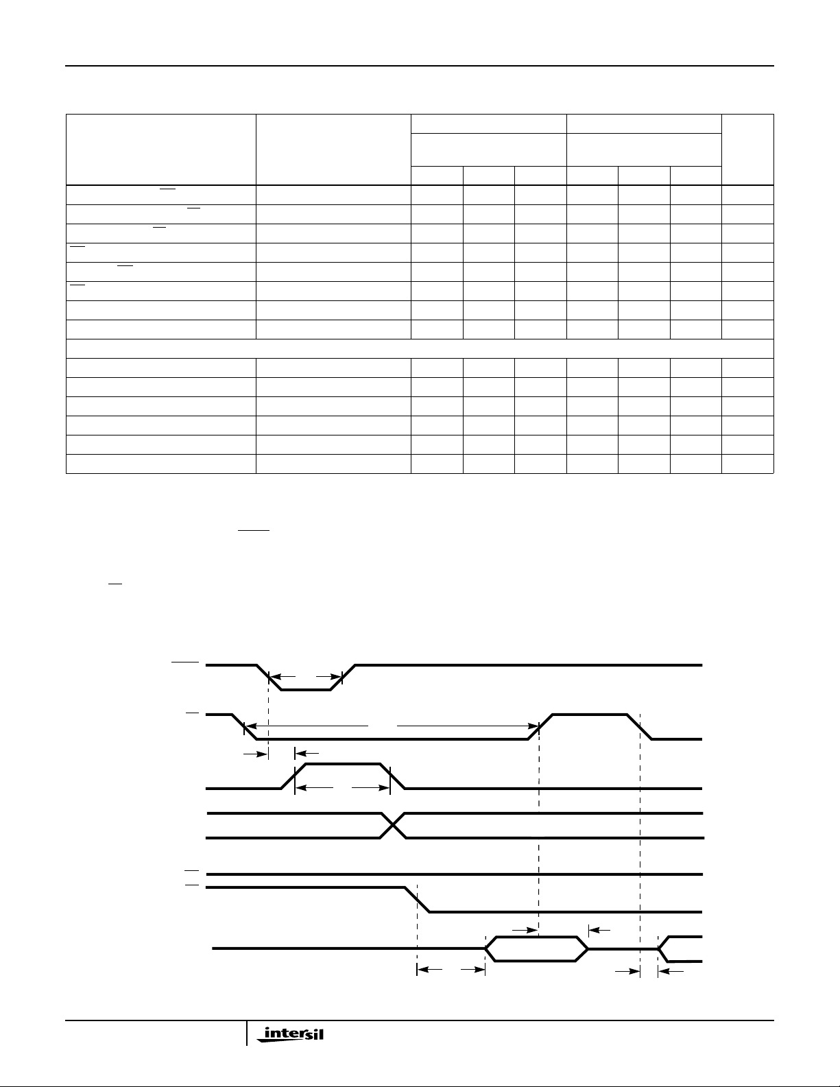
Timing Diagrams
CONV
CS
IRQ
DATA VALID
AO
OE
D0 - D11, OVF
ACQUIRE N
5
t
1
t
7
N CONVERSION
N - 1 DATA
t
16
t
8
t
12
FIGURE 1. SINGLE SHOT TIMING
N DATA
t
15
N DATA
t
17

Timing Diagrams (Continued)
HI5800
CS
CONV
t
2
t
3
t
1
CS
OE
t
5
t
6
t
4
FIGURE 2A. START CONVERSION SETUP TIME FIGURE 2B. OUTPUT ENABLE SETUP TIME
CONV
CS
t
7
t
11
t
13
N+1 CONVERSION
N DATA
t
14
t
10
N + 1 DATA
IRQ
DATA VALID
AO
OE
N CONVERSION
N - 1 DATA
t
8
ACQUIRE N + 1ACQUIRE N
t
9
D4 - D11
D0 - D11, OVF
FIGURE 3. CONTINUOUS CONVERSION TIMING
Typical Performance Curves
80
70
60
50
40
dB
30
20
10
0
20K 200K 2M
INPUT FREQUENCY (Hz)
D11 - D4 D11 - D4
t
12
D3 - D0, 0000
N DATA
90
80
70
60
50
dB
40
30
20
10
0
20K 200K 2M
D11 - D4
N + 1 DATA
INPUT FREQUENCY (Hz)
FIGURE 4. TYPICAL SNR vs INPUT FREQUENCY FIGURE 5. TYPICAL THD vs INPUT FREQUENCY
6

Typical Performance Curves (Continued)
HI5800
80
70
60
50
40
dB
30
20
10
0
20K 200K 2M
INPUT FREQUENCY (Hz)
90
80
70
60
50
dB
40
30
20
10
0
20K 200K 2M
INPUT FREQUENCY (Hz)
FIGURE 6. TYPICAL SINAD vs INPUT FREQUENCY FIGURE 7. TYPICAL SFDR vs INPUT FREQUENCY
11.5
11.25
11.0
10.75
ENOB
10.5
10.25
10.0
dB
12
10
8
6
4
2
0
20K 200K 2M
INPUT FREQUENCY (Hz)
FIGURE8. TYPICALEFFECTIVE NUMBER OF BITSvs INPUT
FREQUENCY
1.0
0.5
0
DNL ERROR (LSB)
-0.5
-1.0
0 1000 2000 3000 4000
CODE
9.75
0.5 1.0 1.50 2.502.00
V
REF
FIGURE 9. EFFECTIVE NUMBER OF BITS vs REFERENCE
VOLTAGE (fS = 3MHz, fIN = 20kHz)
1.0
0.5
0
INL ERROR (LSB)
-0.5
-1.0
0 1000 2000 3000 4000
CODE
FIGURE 10. DIFFERENTIAL NON-LINEARITY FIGURE 11. INTEGRAL NON-LINEARITY
(V)
7

Typical Performance Curves (Continued)
HI5800
10
0
-25
-50
-75
OUTPUT LEVEL (dB)
-100
-125
-135
0 365K 730K 1.095M 1.46M
FREQUENCY (Hz)
10
0
-25
-50
-75
OUTPUT LEVEL (dB)
-100
-125
-135
0 365K 730K 1.095M 1.46M
FREQUENCY (Hz)
FIGURE 12. FFT SPECTRAL PLOT FOR fIN = 20kHz, fS = 3MHz FIGURE 13. FFT SPECTRAL PLOT FOR fIN = 1MHz, fS = 3MHz
10
0
-25
-50
-75
10
0
-25
-50
49K 50K
-75
-100
OUTPUT LEVEL (dB)
-125
-135
0 365K 730K 1.095M 1.46M
FREQUENCY (Hz)
-100
OUTPUT LEVEL (dB)
-125
-135
0 18.3K 36.6K
55K 73.3K 91.6K 110K
FREQUENCY (Hz)
FIGURE 14. FFT SPECTRAL PLOT FOR fIN = 2MHz, fS = 3MHz FIGURE 15. INTERMODULATION DISTORTION PLOT FOR
fIN = 49kHz, 50kHz at fS = 3MHz
Pin Descriptions
PIN # SYMBOL PIN DESCRIPTION
1 REF
2RO
3RG
4AVCCAnalog Positive Power Supply, +5V.
5 REF
- NC No Connection.
6VINAnalog Input Voltage.
7 AGND Analog Ground.
External Reference Input.
IN
DAC Offset Adjust (Connect to AGND If Not Used).
ADJ
DAC Gain Adjust (Connect to AGND If Not Used).
ADJ
Internal Reference Output, +2.5V.
OUT
8 ADJ+ Sample/Hold Offset Adjust (Connect to AGND If Not Used).
9 ADJ- Sample/Hold Offset Adjust (Connect to AGND If Not Used).
8

HI5800
Pin Descriptions (Continued)
PIN # SYMBOL PIN DESCRIPTION
10 AV
11 AV
12 AGND Analog Ground.
13 AV
14 A0 Output Byte Control Input, active low. When low, data is presented as a 12-bit word or the upper byte (D11 - D4) in 8-bit
15 CS Chip Select Input, active low. Dominates all control inputs.
- NC No Connection.
16 OE Output Enable Input, active low.
17 CONV Convert Start Input. Initiates conversion on the falling edge. If held low, continuous conversion mode overrides and
18 DV
19 DGND Digital Ground.
20 DV
21 AV
22 D0 Data Bit 0, (LSB).
23 D1 Data Bit 1.
Analog Negative Power Supply, -5V.
EE
Analog Positive Power Supply, +5V.
CC
Analog Negative Power Supply, -5V.
EE
mode. When high, the second byte contains the lower LSBs (D3 - D0) with 4 trailing zeroes. See Text.
remains in effect until the input goes high.
Digital Negative Power Supply, -5V.
EE
Digital Positive Power Supply, +5V.
CC
Analog Positive Power Supply, +5V.
CC
24 D2 Data Bit 2.
25 D3 Data Bit 3.
- NC No Connection
26 D4 Data Bit 4.
27 D5 Data Bit 5.
28 D6 Data Bit 6.
29 D7 Data Bit 7.
30 AV
31 AGND Analog Ground.
32 DGND Digital Ground.
33 DV
34 D8 Data Bit 8.
35 D9 Data Bit 9.
- NC No Connection.
36 D10 Data Bit 10.
37 D11 Data Bit 11 (MSB).
38 AV
39 OVF Overflow Output. Active high when either an overrange or underrange analog input condition is detected.
Analog Negative Power Supply, -5V.
EE
Digital Positive Power Supply, +5V.
CC
Analog Positive Power Supply, +5V.
CC
40 IRQ Interrupt ReQuest Output. Goes low when a conversion is complete.
9

HI5800
Description
The HI5800 is a 12-bit, two-step, sampling analog-to-digital
converter which uses a subranging technique with digital
error correction. As illustrated in the block diagram, it uses a
sample and hold front end, 7-bit, R-2R D/A converter which
is laser trimmed to 14 bits accuracy, a 7-bit BiCMOS flash
converter,precision bandgap reference,digital controller and
timing generator, error correction logic, output latches and
BiCMOS output drivers.
The falling edge of the convert command signal puts the
sample and hold (S/H) in the hold mode and the conversion
process begins. At this point the Interrupt Request (IRQ) line is
set high indicating that a conversion is in progress. The output
of the S/H circuit drives the input of the 7-bit flash converter
through a switch. After allowing the flash to settle, the
intermediate output of the flash is stored in the latches which
feed the D/A and error correction logic. The D/A reconstructs
the analog signal and feeds the gain amplifier whose summing
node subtracts the held signal of the S/H and amplifies the
residue by 32. This signal is then switched to the flash f or a
second pass using the input switch. The output of the second
flash conversion is f ed directly to the error correction which
reconstructs the twelve bit word from the fourteen bit input. The
logic also decodes the overflow bit and the polarity of the
overflow. The output of the error correction is then gated
through the read controller to the output drivers. The data is
ready on the bus as soon as the IRQ line goes low.
I/O Control Inputs
The converter has four active low inputs (CS, CONV,OE and
A0) and fourteen outputs (D0 - D11, IRQ and OVF). All
inputs and outputs are TTL compatible and will also interface
to the newer TTL compatible families. All four inputs are
CMOS high input impedance stages and all outputs are
BiMOS drivers capable of driving 100pF loads.
In order to initiate a conversion or read the data bus,
be held low.The conversion is initiated bythe fallingedge of the
CONV command. The OE input controls the output bus directly
and is independent of the conversion process. The data on the
bus changes just before the IRQ goes low. Therefore if the
line is held low all the time, the data on the bus will change just
before the IRQ line goes low. The byte control signal
independent of the conversion process and the byte can be
manipulated anytime. When
word is read on the bus. The bus can also be hook ed up such
that the upper byte (D11 - D4) is read when
is high, the lower byte (D3 - D0) is output on the same eight
pins with trailing zeros.
In order to minimize switching noise during a conversion,
byte manipulations done using the
in the single shot mode and
the acquisition phase. For accuracy, allow sufficient time for
settling from any glitches before the next conversion.
Once a conversion is started, the converter will complete the
conversion and acquisition periods irrespective of the input
A0 is low the 12-bits and overflow
A0 is low.When A0
A0 signal should be done
A0 should be changed during
CS should
OE
A0 is also
states. If during these cycles another convert command is
issued, it will be ignored until the acquire phase is complete.
Stand Alone Operation
The converter can be operated in a stand alone configuration
with bus inputs controlling the converter. The conversion will be
started on the negative edge of the convert (
long as this pulse is less than the converter throughput rate. If
the converter is given multiple conv ert commands, it will ignore
all but the first command until such time when the acquisition
period of the next cycle is complete. At this point it will start a
new conversion on the first negativ e edge of the input
command. This allows the converter to be synchronized to a
multiple of a faster external clock. The ne w output data of the
conversion is av ailab le on the same cycle at the negative edge
of the IRQ pulse and is valid until the next negative edge of the
IRQ pulse. Data may be accessed at any time during these
cycles. It should be noted that if the data bus is kept enabled all
the time (
the IRQ goes low. During this time,the data may not be validfor
a few nanoseconds.
OE is low), then the data will be updating just before
CONV) pulse as
Continuous Convert Mode
The converter can be operated at its maximum rate by taking
the
CONV line low (supplying the first negative edge) and
holding it low. This enables the continuous convert mode.
During this time, at the end of the internal acquisition period,
the converter automatically starts a new conversion. The
data will be valid between the IRQ negative edges.
Note that there is no pipelinedelay on the data. The output data
is availableduring thesame cycleas theconversionand isvalid
until the next conv ersion ends. This allo ws data access to both
previous and present conv ersions in the same cycle.
When initiating a conversion or a series of conversions, the
last signal (
The same condition holds true for enabling the bus to read
the data (
first signal (
CS and CONV) to arrive dominates the function.
CS and OE). To terminate the bus operations, the
CS and OE) to arrive dominates the function.
Interrupt Request Output
The interrupt request line (IRQ) goes high at the start of each
conversionand goes low to indicate the start of the acquisition.
During the time that IRQ is high, the internal sample and hold is
in hold mode. At the termination of IRQ, the sample and hold
switches to acquire mode which lasts approximately 100ns. If
no convert command is issued for a period of time, the sample
and hold simply remains in acquire mode tracking the analog
input signal until the next conv ersion cycle is initiated. The IRQ
line is the only output that is not three-stateable.
Analog Input, V
The analog input of the HI5800 is coupled into the input
stage of the Sample and Hold amplifier. The input is a high
impedance bipolar differential pair complete with an ESD
protection circuit. Typically it has >3MΩ input impedance.
With this high input impedance circuit, the HI5800 is easily
IN
10

HI5800
interfaced to any type of op amp without a requirement for a
high drive capability. Adequate precautions should be taken
while driving the input from high voltage output op amps to
ensure that the analog input pin is not overdriven above the
specified maximum limits. For a +2.5V reference, the analog
input range is ±2.5V. This input range scales with the value
of the external reference voltage if the internal reference is
not used. For best performance, the analog ground pin next
to the analog input should be utilized for signal return.
Figures 16 and 17 illustrate the use of an input buffer as a
level shifter to convert a unipolar signal to the bipolar input
used by the HI5800. Figure 16 is an example of a noninverting buffer that takes a 0 to 2.5V input and shifts it to
±2.5V. The gain can be calculated from:
IN
R1
---------------------R1 R3+
1kΩ
+15V
-
+
-15V
R2
V
×–=
0.1
HA2841
0.1
OFFSET
V
OUT
HI5800
V
IN
V
OUT
V
OFFSET
R1||R
R2
1
------------------------ -+ VIN×
R1||R3()
R1R3
----------------------=
3
R1 R3+
R3
2kΩ
R1
2kΩ
V
FIGURE 16. NON-INVERTING BUFFER
Figure 17 is an example of an inverting bufferthat levelshifts
a 0V to 5V input to ±2.5V. Its gain can be calculated from:
V
OFFSET
V
OUT
V
IN
R2– R1⁄()VIN× R2 R3⁄()V
+15V
-15V
R2
1kΩ
0.1
-
+
HA2841
0.1
R1
1kΩ
R3
2kΩ
FIGURE 17. INVERTING BUFFER
OFFSET
V
OUT
.×–=
HI5800
V
IN
Note that the correct op amp must be chosen in order to not
degrade the overall dynamic performance of the circuit.
Recommended op amps are called out in the figures.
Voltage Reference, REF
OUT
The HI5800 has a curvature corrected internal band-gap
referencegenerator with a bufferamplifier capable of driving up
to 15mA. The band-gap and amplifier are trimmed to give
+2.50V.When connected to the reference input pin REF
, the
IN
reference is capable of driving up to 2mA externally. Further
loading may degrade the perf ormance of the output voltage . It
is recommended that the output of the reference be decoupled
with good quality capacitors to reduce the high frequency noise.
Reference Input, REF
IN
The converter requires a voltage reference connected to the
pin. This can be the above internal reference or it can
REF
IN
be an external reference. It is recommended that adequate
high frequency decoupling is provided at the reference input
pin in order to minimize overall converter noise.
A user trying to provide an external reference to a HI5800 is
faced with two problems. First, the drift of the reference over
temperature must be very low.Second, it must be capable of
driving the 200Ω input impedance seen at the REF
pin of
IN
the HI5800. Figure 18 is a recommended circuit for doing
this that is capable of 2ppm/
V
OUTVFB
+15V
10µ
+
REF101
R
R
C
0.1
FIGURE 18. EXTERNAL REFERENCE
B
LOW TC RESISTOR
o
C drift over temperature.
HA5177 HA5002
+15 +15
10
kΩ
+
-
-15 -15
A
10Ω
+
10µ 0.1
HI5800
REF
IN
Supply and Ground Considerations
The HI5800 has separate analog and digital supply and
ground pins to help keep digital noise out of the analog signal
path. For the best performance, the part should be mounted
on a board that provides separate low impedance planes for
the analog and digital supplies and grounds. Only connect the
two grounds together at one place preferab ly as close as
possible to the part. The supplies should be driven by clean
linear regulated supplies. The board should also have good
high frequency decoupling capacitors mounted as close as
possible to the HI5800.
If the part is powered off a single supply then the analog
supply and ground pins should be isolated by ferrite beads
from the digital supply and ground pins.
Also, it is recommended that the turn-on power supply
sequencing be such that the analog positive supply, AI
CC
,
come up first, followed by the remaining supplies.
Refer to the Application Note “Using Intersil High Speed A/D
Converters” (AN9214) for additional suggestions to consider
when using the HI5800.
Error Adjustments
For most applications the accuracy of the HI5800 is sufficient
without any adjustments. In applications where accuracy is of
utmost importance three external adjustments are possible:
S/H offset, D/A offset and D/A gain. Figure 19 illustrates the use
of external potentiometers to reduce the HI5800 errors to zero.
The D/A offset (RO
trims adjust the voltage offset of the transfer curve while the
) and S/H offset (ADJ+ and ADJ-)
ADJ
11

HI5800
D/A gain trim (RG
) adjusts the tilt of the transfer curve
ADJ
around the curve midpoint (code 2048). The 10kΩ
potentiometers can be installed to achieve the desired
adjustment in the following manner.
Typically only one of the offset trimpots needs to be used.
The offset should first be adjusted to get code 2048 centered
at a desired DC input voltage such as 0V. Next the gain trim
can be adjusted by trimming the gain pot until the 4094 to
4095 code transition occurs at the desired voltage
V
CC
(2.500V - 1.5 LSBs for a 2.5V reference). The gain trim can
also be done by adjusting the gain pot until the code 0 to 1
10kΩ
10kΩ
RO
RG
ADJ
ADJ
transition occurs at a particular voltage (-2.5V + 0.5 LSBs for
a 2.5V reference). If a nonzero offset is needed, then the
offset pot can be adjusted after the gain trim is finished. The
gain trim is simplified if an offset trim to zero is done first with
a nonzero offset trim done after the gain trim is finished. The
V
EE
D/A offset and S/H offset trimpots have an identical effect on
the converter except that the S/H offset is a finer resolution
ADJ+
10kΩ
V
EE
FIGURE 19. D/A OFFSET, D/A GAIN AND S/H OFFSET
ADJUSTMENTS
INPUTS OUTPUT
1XXXXNo operation.
0 0 X X X Continuous convert mode.
0 X 0 0 X Outputs all 12-bits and OVF or upper byte D11 - D4 in 8 bit mode.
0 X 0 1 X In 8-bit mode, outputs lower LSBs D3 - D0 followed by 4 trailing zeroes
0 1 X X 0 Converter is in acquisition mode.
0 X X X 1 Converter is busy doing a conversion.
0 X 1 X X Data outputs and OVF in high impedance state.
X’s = Don’t Care
ADJ-
TABLE 1. I/O TRUTH TABLE
trim. The D/A offset and D/A gain typically have an
adjustment range of ±30 LSBs and the S/H offset typically
has an adjustment range of ±20 LSBs.
FUNCTIONCS CONV OE A0 IRQ
and OVF (See text).
TABLE 2. A/D OUTPUT CODE TABLE
CODE
DESCRIPTION
2 (REFIN)
LSB =
≥+FS (Full Scale) ≥ +2.5000 1 1 1 1 1 1 1 1 1 1 1 1 1
NOTE: The voltages listed above represent the ideal center of each output code shown as a function of the reference voltage.
4096
+FS - 1 LSB +2.49878 0 1 1 1 1 1 1 1 1 1 1 1 1
+3/4 FS +1.8750 0 1 1 1 0 0 0 0 0 0 0 0 0
+1/2 FS +1.2500 0 1 1 0 0 0 0 0 0 0 0 0 0
+1 LSB +0.00122 0 1 0 0 0 0 0 0 0 0 0 0 1
0 0.0000 0 1 0 0 0 0 0 0 0 0 0 0 0
-1 LSB -0.00122 0 0 1 1 1 1 1 1 1 1 1 1 1
-1/2 FS -1.2500 0 0 1 0 0 0 0 0 0 0 0 0 0
-3/4 FS -1.8750 0 0 0 1 0 0 0 0 0 0 0 0 0
-FS + 1 LSB -2.49878 0 0 0 0 0 0 0 0 0 0 0 0 1
≤-FS ≤ -2.5000 1 0 0 0 0 0 0 0 0 0 0 0 0
(NOTE)
INPUT
VOLTAGE
= 2.5V
REF
IN
(V)
MSB LSB
OVF D11 D10 D9 D8 D7 D6 D5 D4 D3 D2 D1 D0
OUTPUT DATA (OFFSET BINARY)
12

HI5800
If no external adjustments are required the following pins
should be connected to analog ground (AGND) for optimum
performance: RO
ADJ
, RG
, ADJ+, and ADJ-.
ADJ
Typical Application Schematic
A typical application schematic diagram for the HI5800 is
shown with the block diagram. The adjust pins are shown
with 10kΩ potentiometers used for gain and offset
adjustments. These potentiometers may be left out and the
respective pins should be connected to ground for best
untrimmed performance.
Definitions
Static Performance Definitions
Offset, Full scale, and gain all use a measured value of the
internal voltage reference to determine the ideal plus and
minus full scale values. The results are all displayedin LSBs.
Offset Error (VOS)
The first code transition should occur at a level1/2 LSB
above the negative full scale. Offset is defined as the
deviation of the actual code transition from this point. Note
that this is adjustable to zero.
Full Scale Error (FSE)
The last code transition should occur for a analog input that
1
is 1
/2 LSBs below positive full scale. Full scale error is
defined as the deviation of the actual code transition from
this point.
Differential Linearity Error (DNL)
DNL is the worst case deviation of a code width from the
ideal value of 1 LSB. The converter is guaranteed for no
missing codes over all temperature ranges.
Integral Linearity Error (INL)
INL is the worst case deviation of a code center from a best
fit straight line calculated from the measured data.
Power Supply Rejection (PSRR)
Each of the power supplies are moved plus and minus 5%
and the shift in the offset and full scale error is noted. The
number reported is the percent change in these parameters
versus full scale divided by the percent change in the supply.
Dynamic Performance Definitions
Fast Fourier Transform (FFT) techniques are used to
evaluate the dynamic performance of the HI5800. A low
distortion sine waveis applied to the input, it is sampled, and
the output is stored in RAM. The data is then transformed
into the frequency domain with a 4096 point FFT and
analyzed to evaluate the dynamic performance of the A/D.
The sine waveinput to the part is -0.5dB down from full scale
for all these tests. Distortion results are quoted in dBc
(decibels with respect to carrier) and DO NOT include any
correction factors for normalizing to full scale.
Signal-to-Noise Ratio (SNR)
SNR is the measured RMS signal to RMS noise at a
specified input and sampling frequency. The noise is the
RMS sum of all of the spectral components except the
fundamental and the first five harmonics.
Signal-to-Noise + Distortion Ratio (SINAD)
SINAD is the measured RMS signal to RMS sum of all other
spectral components below the Nyquist frequency excluding
DC.
Effective Number Of Bits (ENOB)
The effective number of bits (ENOB) is derived from the
SINAD data. ENOB is calculated from:
ENOB = (SINAD - 1.76 + V
where: V
CORR
= 0.5dB.
CORR
) / 6.02,
Total Harmonic Distortion (THD)
THD is the ratio of the RMS sum of the first 5 harmonic
components to the RMS value of the measured input signal.
Spurious Free Dynamic Range (SFDR)
SFDR is the ratio of the fundamental RMS amplitude to the
RMS amplitude of the next largest spur or spectral
component. If the harmonics are buried in the noise floor it is
the largest peak.
Intermodulation Distortion (IMD)
Nonlinearities in the signal path will tend to generate
intermodulation products when two tones, f
present on the inputs. The ratio of the measured signal to
the distortion terms is calculated. The IMD products used to
calculate the total distortion are (f
(2f
), (2f2-f1), (2f2+f1), (3f1-f2), (3f1+f2), (3f2-f1), (3f2+f1),
1+f2
(2f
-2f1), (2f2+2f1), (2f1), (2f2), (2f1), (2f2), (4f1), (4f2). The
2
data reflects the sum of all the IMD products.
2-f1
and f2, are
1
), (f2+f1), (2f1-f2),
Full Power Input Bandwidth
Full power input bandwidth is the frequency at which the
amplitude of the fundamental of the digital output word has
decreased 3dB below the amplitude of an input sine wave.
The input sine wave has a peak-to-peak amplitude equal to
the reference voltage. The bandwidth given is measured at
the specified sampling frequency.
13

Die Characteristics
HI5800
DIE DIMENSIONS:
202 mils x 283 mils x 19 mils
METALLIZATION:
Metal 1: Type: AlSiCu, Thickness: 6k
Å +1500A/-750Å
Metal 2: Type: AlSiCu, Thickness: 16kÅ+2500A/-1100Å
Metallization Mask Layout
VCC
VCC
REF_OUT
A
A
V
AGND
AGND
ADJ+
ADJ-
AV
EE
AV
EE
AV
CC
AV
CC
AGND
REF_OUT
IN
RG_ADJ
HI5800
RO_ADJ
PASSIVATION:
Type: Sandwich P assivation - Nitride +
Undoped Si Glass (USG)
Thickness: Nitride - 4K
Å, USG - 8KÅ, Total - 12kű2kÅ
TRANSISTOR COUNT:
10K
SUBSTRATE POTENTIAL (POWERED UP):
V
EE
REF_IN
IRQ
VCC
D11 (MSB)
A
OVF
D10
D9
D8
D
VCC
DGND
AGND
V
EE
AV
AV
EE
EE
A0
CS
14
OE
CONV
DV
EE
DGND
DGND
DV
CC
DV
CC
CC
AV
D6 (LSB)
D1
D2
D7
D6
D5
D4
D3

HI5800
Ceramic Dual-In-Line Metal Seal Packages (SBDIP)
LEAD FINISH
c1
-A-
-B-
S
bbb C A - B
BASE
PLANE
SEATING
PLANE
S1
b2
ccc
b
C A - BM
D
A
A
e
DS S
NOTES:
1. Indexarea: Anotchora pin one identification mark shall belocated adjacent to pin one and shall be located within the shaded
area shown. The manufacturer’s identification shall not be used
as a pin one identification mark.
2. The maximum limits of lead dimensions b and c or M shall be
measured at the centroid of the finished lead surfaces, when
solder dip or tin plate lead finish is applied.
3. Dimensionsb1 and c1 apply to lead base metal only. Dimension
M applies to lead plating and finish thickness.
4. Corner leads (1, N, N/2, and N/2+1) may be configured with a
partial lead paddle. For this configuration dimension b3 replaces
dimension b2.
5. Dimension Q shall be measured from the seating plane to the
base plane.
6. Measure dimension S1 at all four corners.
7. Measure dimension S2 from the top of the ceramic body to the
nearest metallization or lead.
8. N is the maximum number of terminal positions.
9. Braze fillets shall be concave.
10. Dimensioning and tolerancing per ANSI Y14.5M - 1982.
11. Controlling dimension: INCH.
-DBASE
E
S
S
D
Q
S2
-C-
METAL
b1
M
(b)
SECTION A-A
A
L
(c)
M
eA
aaa
eA/2
C A - BM DS S
c
D40.6 MIL-STD-1835 CDIP2-T40 (D-5, CONFIGURATION C)
40 LEAD CERAMIC DUAL-IN-LINE METAL SEAL PACKAGE
INCHES MILLIMETERS
SYMBOL
A - 0.225 - 5.72 -
b 0.014 0.026 0.36 0.66 2
b1 0.014 0.023 0.36 0.58 3
b2 0.045 0.065 1.14 1.65 b3 0.023 0.045 0.58 1.14 4
c 0.008 0.018 0.20 0.46 2
c1 0.008 0.015 0.20 0.38 3
D - 2.096 - 53.24 4
E 0.510 0.620 12.95 15.75 4
e 0.100 BSC 2.54 BSC -
eA 0.600 BSC 15.24 BSC -
eA/2 0.300 BSC 7.62 BSC -
L 0.125 0.200 3.18 5.08 -
Q 0.015 0.070 0.38 1.78 5
S1 0.005 - 0.13 - 6
S2 0.005 - 0.13 - 7
o
α
90
105
o
90
o
105
aaa - 0.015 - 0.38 bbb - 0.030 - 0.76 ccc - 0.010 - 0.25 -
M - 0.0015 - 0.038 2
N40 408
NOTESMIN MAX MIN MAX
o
Rev. 0 4/94
-
All Intersil semiconductor products are manufactured, assembled and tested under ISO9000 quality systems certification.
Intersil semiconductor products are sold by description only. Intersil Corporation reserves the right to make changes in circuit design and/or specifications at any time without notice. Accordingly, the reader is cautioned to verify that data sheets are current before placing orders. Information furnished by Intersil is believed to be accurate and
reliable. However,no responsibility is assumed by Intersil or its subsidiaries for its use; nor for any infringements of patents or other rights of third parties which may result
from its use. No license is granted by implication or otherwise under any patent or patent rights of Intersil or its subsidiaries.
For information regarding Intersil Corporation and its products, see web site http://www.intersil.com
Sales Office Headquarters
NORTH AMERICA
Intersil Corporation
P. O. Box 883, Mail Stop 53-204
Melbourne, FL 32902
TEL: (321) 724-7000
FAX: (321) 724-7240
15
EUROPE
Intersil SA
Mercure Center
100, Rue de la Fusee
1130 Brussels, Belgium
TEL: (32) 2.724.2111
FAX: (32) 2.724.22.05
ASIA
Intersil (Taiwan) Ltd.
7F-6, No. 101 Fu Hsing North Road
Taipei, Taiwan
Republic of China
TEL: (886) 2 2716 9310
FAX: (886) 2 2715 3029
 Loading...