

HI5728
Data Sheet July 1999
10-Bit, 125/60MSPS, Dual High Speed
CMOS D/A Converter
The HI5728 is a 10-bit, dual 125MSPS D/A converter which
is implemented in an advanced CMOS process. It is
designed for high speed applications where integration,
bandwidth and accuracy are essential. Operating from a
single +5V or +3V supply, the converter provides20.48mAof
full scale output current and includes an input data register.
Low glitch energy and excellent frequency domain
performance are achieved using a segmented architecture.
A 60MSPS version and an 8-bit (HI5628) version are also
available. Comparable single DAC solutions are the HI5760
(10-bit) and the HI5660 (8-bit). This DACis a member of the
CommLink™ family of communication devices.
Ordering Information
TEMP.
PART
NUMBER
RANGE
(oC) PACKAGE PKG. NO.
HI5728IN -40 to 85 48 Ld LQFP Q48.7x7A 125MHz
HI5728/6IN -40 to 85 48 Ld LQFP Q48.7x7A 60MHz
HI5728EVAL1 25 Evaluation Platform 125MHz
MAX
CLOCK
SPEED
File Number 4321.4
Features
• Throughput Rate . . . . . . . . . . . . . . . . . . . . . . . .125MSPS
• Low Power . . . . . . . . . . . . . . . 330mW at 5V, 54mW at 3V
• Integral Linearity Error . . . . . . . . . . . . . . . . . . . . . ±1 LSB
• Differential Linearity . . . . . . . . . . . . . . . . . . . . . . ±0.5 LSB
• Gain Matching (Typ). . . . . . . . . . . . . . . . . . . . . . . . . .0.5%
• SFDR at 5MHz Output . . . . . . . . . . . . . . . . . . . . . . .68dBc
• Single Power Supply from +5V to +3V
• CMOS Compatible Inputs
• Excellent Spurious Free Dynamic Range
• Internal Voltage Reference
• Dual 10-Bit D/A Converters on a Monolithic Chip
Applications
• Wireless Local Loop
• Direct Digital Frequency Synthesis
• Wireless Communications
• Signal Reconstruction
• Arbitrary Waveform Generators
• Test Equipment/Instrumentation
• High Resolution Imaging Systems
Pinout
ID6
ID5
ID4
ID3
ID2
ID1
ID0 (LSB)
SLEEP
DV
DD
DGND
NC
AV
DD
ID8
ID7
1
2
3
4
5
6
7
8
9
10
11
12
13 14 15 16
AGND
ICOMP1
TOP VIEW
DD
DV
ID9 (MSB)
DGND
IOUTA
IOUTB
REFLO
HI5728
(LQFP)
ICLK
AGND
QCLK
AGND
QOUTB
DV
DGND
QOUTA
DD
QD9 (MSB)
FSADJ
QD8
QD7
373839404142434445464748
36
35
34
33
32
31
30
29
28
27
26
25
2423222120191817
REFIO
QCOMP1
QD6
QD5
QD4
QD3
QD2
QD1
QD0 (LSB)
DV
DD
DGND
NC
AV
DD
AGND
1
CAUTION: These devices are sensitive to electrostatic discharge; follow proper IC Handling Procedures.
1-888-INTERSIL or 321-724-7143
CommLink™ is a trademark of Intersil Corporation.
| Copyright © Intersil Corporation 1999
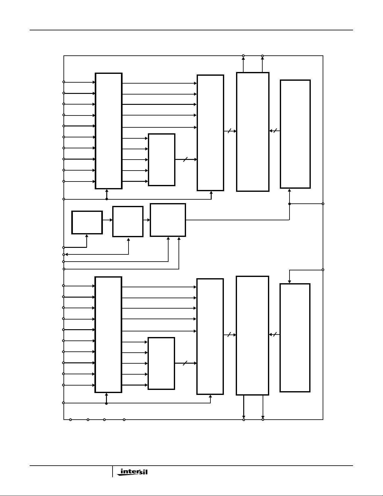
Functional Block Diagram
(LSB) ID0
ID1
ID2
HI5728
IOUTA IOUTB
CASCODE
CURRENT
SOURCE
ID3
ID4
ID5
ID6
ID7
ID8
(MSB) ID9
ICLK
REFLO
REFIO
FSADJ
SLEEP
(LSB) QD0
QD1
QD2
INT/EXT
REFERENCE
SELECT
LATCH
INT/EXT
VOLTAGE
REFERENCE
UPPER
5-BIT
DECODER
BIAS
GENERATION
5 LSBs
36
LATCH
31
SWITCH
MATRIX
36
+
31 MSB
SEGMENTS
CASCODE
CURRENT
SOURCE
ICOMP1
QCOMP1
QD3
QD4
QD5
QD6
QD7
QD8
QCLK
AV
DD
AGND
LATCH
DV
DD
2
DGND
UPPER
5-BIT
DECODER
5 LSBs
36
LATCH
31
SWITCH
MATRIX
QOUTA QOUTB
36
+
31 MSB
SEGMENTS
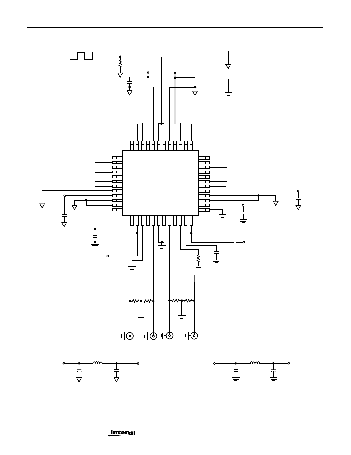
Typical Applications Circuit
50Ω
DV
0.1µF
ID7
DD
ID8
ID9 (MSB)
HI5728
I
CLK/QCLK
DV
DD
0.1µF
QD8
QD7
QD9 (MSB)
DIGITAL
GROUND
PLANE
ANALOG
GROUND
PLANE
SLEEP
DV
DD
0.1µF
ID6
ID5
ID4
ID3
ID2
ID1
ID0 (LSB)
AV
AV
0.1µF
DD
DD
0.1µF
1
2
3
4
5
6
7
8
DV
9
DGND
10
11
NC (GROUND)
12
13 14 15 16
AGND
ICOMP1
DD
50Ω
50Ω
DV
DGND
NC (GROUND)
AGND
AV
50Ω
DD
DD
R
2kΩ
50Ω
373839404142434445464748
2423222120191817
SET
AGND
0.1µF
QD6
QD5
QD4
QD3
QD2
QD1
QD0 (LSB)
AV
DD
0.1µF
AV
0.1µF
DD
NOTE: ICOMP1 AND QCOMP1
PINS (24, 14) MUST BE TIED
TOGETHER EXTERNALLY
0.1µF
DV
DD
36
35
34
33
32
31
30
29
28
27
26
25
QCOMP1
REFIO
+5V OR +3V SUPPLY
+
FERRITE
BEAD
10µH
3
IOUTA
DVDD(POWER PLANE)
0.1µF10µF
IOUTB
QOUTB
QOUTA
(POWER PLANE)
AV
DD
0.1µF
FERRITE
BEAD
10µH
+5V OR +3V SUPPLY
+
10µF
HI5728
Pin Descriptions
PIN NO. PIN NAME PIN DESCRIPTION
39-30 QD9 (MSB) Through
QD0 (LSB)
1-6, 48-46 ID9 (MSB) Through
ID0 (LSB)
8 SLEEP ControlPinfor Power-Downmode. SleepModeis activehigh; Connect toground forNormalMode. Sleep
15 REFLO Connect to analog ground to enable internal 1.2V reference or connect to AVDD to disable.
23 REFIO Reference voltage input if internal reference is disabled and reference voltage output if internal ref erence is
22 FSADJ Full Scale Current Adjust. Use a resistor to ground to adjust full scale output current. Full Scale Output
14, 24 ICOMP1, QCOMP1 Reduces noise. Connect each toAVDDwith 0.1µF capacitorneareachpin. The ICOMP1 and QCOMP1
13, 18, 19, 25 AGND Analog Ground Connections.
17 IOUTB The complimentary current output of the I channel. Bits set to all 0s gives full scale current.
16 IOUTA Current output of the I channel. Bits set to all 1s gives full scale current.
20 QOUTB The complimentary current output of the Q channel. Bits set to all 0s gives full scale current.
21 QOUTA Current output of the Q channel. Bits set to all 1s gives full scale current.
11, 27 NC No Connect. Recommended: connect to ground.
12, 26 AV
10, 28, 41, 44 DGND Digital Ground.
9, 29, 40, 45 DV
43 ICLK Clock input for I channel. Positive edge of clock latches data.
42 QCLK Clock input for Q channel. Positive edge of clock latches data.
DD
DD
Digital Data Bit 9, the Most Significant Bit through Digital Data Bit 0, the Least Significant Bit, of the Q
channel.
Digital DataBit 9, theMost Significant BitthroughDigital DataBit0, the LeastSignificant Bit, oftheI channel.
pin has internal 20µA active pull-down current.
enabled. Use 0.1µF cap to ground when internal reference is enabled.
Current Per Channel = 32 x I
pins MUST be tied together externally.
Analog Supply (+2.7V to +5.5V).
Supply voltage for digital circuitry (+2.7V to +5.5V).
FSADJ
.
4
HI5728
Absolute Maximum Ratings Thermal Information
Digital Supply Voltage DVDD to DCOM . . . . . . . . . . . . . . . . . +5.5V
Analog Supply Voltage AVDD to ACOM. . . . . . . . . . . . . . . . . +5.5V
Grounds, ACOM TO DCOM . . . . . . . . . . . . . . . . . . . -0.3V to +0.3V
Digital Input Voltages (D9-D0, CLK, SLEEP). . . . . . . . .DVDD+0.3V
Internal Reference Output Current. . . . . . . . . . . . . . . . . . . . . ±50µA
Reference Input Voltage Range. . . . . . . . . . . . . . . . . . AVDD+0.3V
Analog Output Current (I
) . . . . . . . . . . . . . . . . . . . . . . . . . 24mA
OUT
Operating Conditions
Temperature Range. . . . . . . . . . . . . . . . . . . . . . . . . . -40oC to 85oC
CAUTION: Stresses above those listed in “Absolute Maximum Ratings” may cause permanent damage to the device. This is a stress only rating and operation of the
device at these or any other conditions above those indicated in the operational sections of this specification is not implied.
NOTE:
1. θJA is measured with the component mounted on an evaluation PC board in free air.
Thermal Resistance (Typical, Note 1) θJA(oC/W)
TQFP Package. . . . . . . . . . . . . . . . . . . . . . . . . . . . . 75
Maximum Power Dissipation
TQFP Package. . . . . . . . . . . . . . . . . . . . . . . . . . . . . . . . . .930mW
Maximum Junction Temperature . . . . . . . . . . . . . . . . . . . . . . .150oC
Maximum Storage Temperature Range. . . . . . . . . . -65oC to 150oC
Maximum Lead Temperature (Soldering 10s) . . . . . . . . . . . . .300oC
Electrical Specifications AV
PARAMETER TEST CONDITIONS
SYSTEM PERFORMANCE (Per Channel)
Resolution 10 - - Bits
Integral Linearity Error, INL “Best Fit” Straight Line (Note 7) -1 ±0.5 +1 LSB
Differential Linearity Error, DNL (Note 7) -0.5 ±0.25 +0.5 LSB
Offset Error, I
Offset Drift Coefficient (Note 7) - 0.1 - ppm
Full Scale Gain Error, FSE With External Reference (Notes 2, 7) -10 ±2 +10 % FSR
Full Scale Gain Drift With External Reference (Note 7) - ±50 - ppm
Gain Matching Between Channels -0.5 0.1 0.5 dB
I/Q Channel Isolation F
Output Voltage Compliance Range (Note 3) -0.3 - 1.25 V
Full Scale Output Current, I
DYNAMIC CHARACTERISTICS (Per Channel)
Maximum Clock Rate, f
Output Settling Time, (t
Singlet Glitch Area (Peak Glitch) RL = 25Ω (Note 7) - 35 - pV•s
Output Rise Time Full Scale Step - 1.5 - ns
Output Fall Time Full Scale Step - 1.5 - ns
Output Capacitance -10- pF
Output Noise IOUTFS = 20mA - 50 - pA/√Hz
OS
FS
CLK
) 0.1% (±1 LSB, equivalent to 9 Bits) (Note 7) - 20 - ns
SETT
= DVDD = +5V, V
DD
per channel except for ‘Power Supply Characteristics.’
(Note 7) -0.025 +0.025 % FSR
With Internal Reference (Notes 2, 7) -10 ±1 +10 % FSR
With Internal Reference (Note 7) - ±100 - ppm
= 10MHz - 80 - dB
OUT
(Note 3) 125 - - MHz
0.05% (±1/2 LSB, equivalent to 10 Bits) (Note 7) - 35 - ns
IOUTFS = 2mA - 30 - pA/√Hz
= Internal 1.2V, IOUTFS = 20mA, TA = 25oC for All Typical Values. Data given is
REF
HI5728IN
TA = -40oC TO 85oC
UNITSMIN TYP MAX
FSR/oC
FSR/oC
FSR/oC
2 - 20 mA
5
HI5728
Electrical Specifications AV
= DVDD = +5V, V
DD
= Internal 1.2V, IOUTFS = 20mA, TA = 25oC for All Typical Values. Data given is
REF
per channel except for ‘Power Supply Characteristics.’ (Continued)
HI5728IN
TA = -40oC TO 85oC
PARAMETER TEST CONDITIONS
UNITSMIN TYP MAX
AC CHARACTERISTICS (Per Channel) - HI5728IN - 125MHz
Spurious Free Dynamic Range,
SFDR Within a Window
Total Harmonic Distortion (THD) to
Nyquist
Spurious Free Dynamic Range,
SFDR to Nyquist
f
= 125MSPS, f
CLK
f
= 100MSPS, f
CLK
f
= 60MSPS, f
CLK
f
= 50MSPS, f
CLK
f
= 50MSPS, f
CLK
f
= 100MSPS, f
CLK
f
= 50MSPS, f
CLK
f
= 50MSPS, f
CLK
f
= 125MSPS, f
CLK
f
= 125MSPS, f
CLK
f
= 100MSPS, f
CLK
f
= 100MSPS, f
CLK
f
= 100MSPS, f
CLK
f
= 100MSPS, f
CLK
f
= 60MSPS, f
CLK
f
= 50MSPS, f
CLK
f
= 50MSPS, f
CLK
f
= 50MSPS, f
CLK
f
= 50MSPS, f
CLK
= 32.9MHz, 10MHz Span (Notes 4, 7) - 75 - dBc
OUT
= 5.04MHz, 4MHz Span (Notes 4, 7) - 76 - dBc
OUT
= 10.1MHz, 10MHz Span (Notes 4, 7) - 75 - dBc
OUT
= 5.02MHz, 2MHz Span (Notes 4, 7) - 76 - dBc
OUT
= 1.00MHz, 2MHz Span (Notes 4, 7) - 78 - dBc
OUT
= 2.00MHz (Notes 4, 7) - 71 - dBc
OUT
= 2.00MHz (Notes 4, 7) - 71 - dBc
OUT
= 1.00MHz (Notes 4, 7) - 76 - dBc
OUT
= 32.9MHz, 62.5MHz Span (Notes 4, 7) - 54 - dBc
OUT
= 10.1MHz, 62.5MHz Span (Notes 4, 7) - 64 - dBc
OUT
= 40.4MHz, 50MHz Span (Notes 4, 7) - 52 - dBc
OUT
= 20.2MHz, 50MHz Span (Notes 4, 7) - 60 - dBc
OUT
= 5.04MHz, 50MHz Span (Notes 4, 7) - 68 - dBc
OUT
= 2.51MHz, 50MHz Span (Notes 4, 7) - 74 - dBc
OUT
= 10.1MHz, 30MHz Span (Notes 4, 7) - 63 - dBc
OUT
= 20.2MHz, 25MHz Span (Notes 4, 7) - 55 - dBc
OUT
= 5.02MHz, 25MHz Span (Notes 4, 7) - 68 - dBc
OUT
= 2.51MHz, 25MHz Span (Notes 4, 7) - 73 - dBc
OUT
= 1.00MHz, 25MHz Span (Notes 4, 7) - 73 - dBc
OUT
AC CHARACTERISTICS (Per Channel) - HI5728/6IN - 60MHz
Spurious Free Dynamic Range,
SFDR Within a Window
Total Harmonic Distortion (THD) to
Nyquist
Spurious Free Dynamic Range,
SFDR to Nyquist
f
= 60MSPS, f
CLK
f
= 50MSPS, f
CLK
f
= 50MSPS, f
CLK
f
CLK
f
CLK
f
= 60MSPS, f
CLK
f
= 60MSPS, f
CLK
f
= 50MSPS, f
CLK
f
= 50MSPS, f
CLK
f
= 50MSPS, f
CLK
f
= 50MSPS, f
CLK
f
= 25MSPS, f
CLK
= 50MSPS, f
= 50MSPS, f
= 10.1MHz, 10MHz Span (Notes 4, 7) - 75 - dBc
OUT
= 5.02MHz, 2MHz Span (Notes 4, 7) - 76 - dBc
OUT
= 1.00MHz, 2MHz Span (Notes 4, 7) - 78 - dBc
OUT
= 2.00MHz (Notes 4, 7) - 71 - dBc
OUT
= 1.00MHz (Notes 4, 7) - 76 - dBc
OUT
= 20.2MHz, 30MHz Span (Notes 4, 7) - 56 - dBc
OUT
= 10.1MHz, 30MHz Span (Notes 4, 7) - 63 - dBc
OUT
= 20.2MHz, 25MHz Span (Notes 4, 7) - 55 - dBc
OUT
= 5.02MHz, 25MHz Span (Notes 4, 7) - 68 - dBc
OUT
= 2.51MHz, 25MHz Span (Notes 4, 7) - 73 - dBc
OUT
= 1.00MHz, 25MHz Span (Notes 4, 7) - 73 - dBc
OUT
= 5.02MHz, 25MHz Span (Notes 4, 7) - 71 - dBc
OUT
VOLTAGE REFERENCE
Internal Reference Voltage, V
FSADJ
Voltage at Pin 22 with Internal Reference 1.04 1.16 1.28 V
Internal Reference Voltage Drift - ±60 - ppm/oC
Internal Reference Output Current
- 0.1 - µA
Sink/Source Capability
Reference Input Impedance -1-MΩ
Reference Input Multiplying Bandwidth (Note 7) - 1.4 - MHz
DIGITAL INPUTS D9-D0, CLK (Per Channel)
Input Logic High Voltage with
5V Supply, V
IH
(Note 3) 3.5 5 - V
6

HI5728
Electrical Specifications AV
= DVDD = +5V, V
DD
= Internal 1.2V, IOUTFS = 20mA, TA = 25oC for All Typical Values. Data given is
REF
per channel except for ‘Power Supply Characteristics.’ (Continued)
HI5728IN
TA = -40oC TO 85oC
PARAMETER TEST CONDITIONS
Input Logic High Voltage with
3V Supply, V
IH
Input Logic Low Voltage with
5V Supply, V
IL
Input Logic Low Voltage with
3V Supply, V
Input Logic Current, I
Input Logic Current, I
IL
IH
IL
Digital Input Capacitance, C
(Note 3)s 2.1 3 - V
(Note 3) - 0 1.3 V
(Note 3) - 0 0.9 V
-10 - +10 µA
-10 - +10 µA
IN
-5-pF
UNITSMIN TYP MAX
TIMING CHARACTERISTICS (Per Channel)
Data Setup Time, t
Data Hold Time, t
SU
HLD
Propagation Delay Time, t
CLK Pulse Width, t
PW1
, t
PD
PW2
See Figure 41 (Note 3) 3 - - ns
See Figure 41 (Note 3) 3 - - ns
See Figure 41 - 1 - ns
See Figure 41 (Note 3) 4 - - ns
POWER SUPPLY CHARACTERISTICS
AVDD Power Supply (Notes 8, 9) 2.7 5.0 5.5 V
DVDD Power Supply (Notes 8, 9) 2.7 5.0 5.5 V
Analog Supply Current (I
) (5V or 3V, IOUTFS = 20mA) - 46 60 mA
AVDD
(5V or 3V, IOUTFS = 2mA) - 8 - mA
Digital Supply Current (I
) (5V, IOUTFS = Don’t Care) (Note 5) - 6 10 mA
DVDD
(3V, IOUTFS = Don’t Care) (Note 5) - 3 - mA
Supply Current (I
) Sleep Mode (5V or 3V, IOUTFS = Don’t Care) - 3.2 6 mA
AVDD
Power Dissipation (5V, IOUTFS = 20mA) (Note 6) - 330 - mW
(5V, IOUTFS = 2mA) (Note 6) - 140 - mW
(3V, IOUTFS = 20mA) (Note 6) - 170 - mW
(3V, IOUTFS = 2mA) (Note 6) - 54 - mW
(5V, IOUTFS = 20mA) (Note 10) - 300 - mW
(3.3V, IOUTFS = 20mA) (Note 10) - 150 - mW
(3V, IOUTFS = 20mA) (Note 10) - 135 - mW
Power Supply Rejection Single Supply (Note 7) -0.2 - +0.2 %
FSR/V
NOTES:
2. Gain Error measured as the error in the ratio between the full scale output current and the current through R
(typically 625µA). Ideally the
SET
ratio should be 32.
3. Parameter guaranteed by design or characterization and not production tested.
4. Spectral measurements made with differential coupled transformer and 100% amplitude.
5. Measured with the clock at 50MSPS and the output frequency at 1MHz, both channels.
6. Measured with the clock at 100MSPS and the output frequency at 40MHz, both channels.
7. See ‘Definition of Specifications’.
8. For operation below 3V, it is recommended that the output current be reduced to 12mA or less to maintain optimum performance. DVDDand
AVDD do not have to be equal.
9. Foroperation above 125MHz, it is recommended that the power supply be 3.3V or greater. The part is functional with the clock above 125MSPS
and the power supply below 3.3V, but performance is degraded.
10. Measured with the clock at 60MSPS and the output frequency at 10MHz, both channels.
7

HI5728
Typical Performance Curves, 5 Volt Power Supply
80
75
70
65
SFDR (dBc)
60
55
50
0 0.2 0.4 0.6 0.8 1 1.2 1.4 1.6 1.8 2
-12dBFS
OUTPUT FREQUENCY (MHz)
FIGURE 1. SFDR vs f
80
0dBFS
75
70
65
SFDR (dBc)
-12dBFS
60
0dBFS
OUT
-6dBFS
-6dBFS
, CLOCK = 5MSPS FIGURE 2. SFDR vs f
76
74
72
70
68
SFDR (dBc)
66
64
62
60
12345678910
75
70
65
-12dBFS
60
SFDR (dBc)
55
50
-12dBFS
OUTPUT FREQUENCY (MHz)
, CLOCK = 25MSPS
OUT
-6dBFS
0dBFS
-6dBFS
0dBFS
55
0 2 4 6 8 101214161820
OUTPUT FREQUENCY (MHz)
FIGURE 3. SFDR vs f
75
70
65
-12dBFS
60
SFDR (dBc)
55
50
45
0 5 10 15 20 25 30 35 40 45 50
OUTPUT FREQUENCY (MHz)
FIGURE 5. SFDR vs f
, CLOCK = 50MSPS FIGURE 4. SFDR vs f
OUT
6dBFS
0dBFS
, CLOCK = 125MSPS FIGURE 6. SFDR vs AMPLITUDE, f
OUT
45
0 5 10 15 20 25 30 35 40 45
OUTPUT FREQUENCY (MHz)
, CLOCK =100MSPS
OUT
80
75
70
65
60
SFDR (dBc)
55
50
45
-25 -20 -15 -10 -5 0
125MSPS
AMPLITUDE (dBFS)
25MSPS
100MSPS
CLK/fOUT
50MSPS
= 10
8

HI5728
Typical Performance Curves, 5 Volt Power Supply (Continued)
80
75
70
65
60
55
SFDR (dBc)
50
45
40
-25 -20 -15 -10 -5 0
AMPLITUDE (dBFS)
100MSPS
FIGURE 7. SFDR vs AMPLITUDE, f
75
70
65
60
55
SFDR (dBc)
50
45
40
2 4 6 8 10 12 14 16 18 20
(mA)
I
OUT
25MSPS
125MSPS
CLK/fOUT
2.5MHz
10MHz
20MHz
50MSPS
= 5 FIGURE 8. SFDR vs AMPLITUDE OF TWO TONES, f
40MHz
75
25MSPS
70
65
60
55
SFDR (dBc)
50
45
40
-25 -20 -15 -10 -5 0
AMPLITUDE (TOTAL PEAK POWER OF COMBINED TONES) (dBFS)
(3.38/3.63MHz)
50MSPS
(6.75/7.25MHz)
100MSPS
(13.5/14.5MHz)
125MSPS
(16.9/18.1MHz)
CLK/fOUT
75
70
65
60
SFDR (dBc)
55
50
45
0 5 10 15 20 25 30 35 40
-6dBFS DIFF
0dBFS DIFF
-6dBFS SINGLE
0dBFS SINGLE
OUTPUT FREQUENCY (MHz)
=7
FIGURE 9. SFDR vs I
, CLOCK = 100MSPS FIGURE 10. DIFFERENTIAL vs SINGLE-ENDED,
OUT
CLOCK = 100MSPS
80
75
70
65
60
55
SFDR (dBc)
50
45
40
-40 -20 0 20 40 60 80
TEMPERATURE (
o
C)
2.5MHz
10.1MHz
40.4MHz
-10
-10
-20
-20
-30
-30
-40
-40
-50
-50
-60
-60
-70
-70
AMP (dB)
Amp (dB)
-80
-80
-90
-90
-100
-100
-110
-110
0
0 5MHz/div 50
14dB EXTERNAL ANALYZER ATTENUATION
14dB External Analyzer Attenuation
5MHz/DIV
Frequency (MHz)
FREQUENCY (MHz)
f
CLK
= 100MSPS
Fout = 9.95MHz
AMPLITUDE = 0dBFS
Amplitude = 0dBFS
SFDR = 64dBc
FIGURE 11. SFDR vs TEMPERATURE, CLOCK = 100MSPS FIGURE 12. SINGLE TONE SFDR
9
= 100MSPS
f
=9.95MHz
OUT
SFDR = 64dBc
50

HI5728
Typical Performance Curves, 5 Volt Power Supply (Continued)
-20
-20
Fclk = 100MSPS
f
= 100MSPS
-30
-30
-40
-40
-50
-50
-60
-60
-70
-70
AMP (dB)
Amp (dB)
-80
-80
-90
-90
-100
-100
-110
-110
0 5MHz/div 50
0
Combined Peak Amplitude = 0dBFS
14dB External Analyzer Attenuation
ANALYZER ATTENUATION
5MHz/DIV
Frequency (MHz)
FREQUENCY (MHz)
CLK
Fout = 13.5/14.5MHz
f
= 13.5/14.5MHZ
OUT
COMBINED PEAK
MTPR = 62.9dBc
AMPLITUDE = 0dBFS
SFDR = 62.9dBc
14dB EXTERNAL
50
-10
-20
-30
-40
-50
-60
AMP (dB)
-70
-80
-90
-100
0.5
f
OUT
1.45MHz/ DIV
FIGURE 13. TWO TONE, CLOCK = 100MSPS FIGURE 14. FOUR-TONE, CLOCK = 100MSPS
-20
-30
-40
-50
-60
-70
AMP (dB)
-80
-90
-100
-110
0.5
= 100MSPS
f
= 2.6,3.2,3.8,4.4,5.6,6.2,6.8MHZ
f
OUT
COMBINED PEAK AMPLITUDE = 0dBFS
SFDR = 67dBc (IN A WINDOW)
1.95MHz/DIV 20
FREQUENCY (MHz)
CLK
-10
-20
-30
-40
-50
-60
AMP (dB)
-70
-80
-90
-100
0.5 950kHz/DIV 10
FREQUENCY (MHz)
f
OUT
f
= 100MSPS
CLK
= 3.8,4.4,5.6,6.2MHz
COMBINED PEAK
AMPLITUDE = 0dBFS
SFDR = 71.4dBc
(IN A WINDOW)
f
= 50MSPS
CLK
= 1.9,2.2,2.8,3.1MHZ
COMBINED PEAK
AMPLITUDE = 0dBFS
SFDR = 73.6dBc
(IN A WINDOW)
15
FIGURE 15. EIGHT-TONE, CLOCK = 100MSPS FIGURE 16. FOUR-TONE, CLOCK = 50MSPS
0.4
0.2
0
LSB
-0.2
-0.4
0 200 400 600 800 1000
CODE
0.4
0.2
0
LSB
-0.2
-0.4
0 200 400 600 800 1000
CODE
FIGURE 17. DIFFERENTIAL NONLINEARITY FIGURE 18. INTEGRAL NONLINEARITY
10

HI5728
Typical Performance Curves, 5 Volt Power Supply (Continued)
320
310
300
290
280
270
260
250
POWER (mW)
240
230
220
210
0 20 40 60 80 100 120
CLOCK RATE (MSPS)
FIGURE 19. POWER vs CLOCK RATE, f
Typical Performance Curves, 3V Power Supply
80
75
70
65
SFDR (dBc)
60
-12dBFS
55
50
0 0.2 0.4 0.6 0.8 1 1.2 1.4 1.6 1.8 2
OUTPUT FREQUENCY (MHz)
FIGURE 20. SFDR vs f
80
75
-6dBFS
70
-12dBFS
65
SFDR (dBc)
60
55
0dBFS
, CLOCK = 5MSPS FIGURE 21. SFDR vs f
OUT
0dBFS
-6dBFS
CLK/fOUT
= 10, I
80
75
70
SFDR (dBc)
65
60
1 2 3 4 5 6 7 8 9 10
80
75
70
65
-12dBFS
60
SFDR (dBc)
55
50
= 20mA
OUT
0dBFS
-12dBFS
OUTPUT FREQUENCY (MHz)
0dBFS
-6dBFS
-6dBFS
, CLOCK = 25MSPS
OUT
50
0 2 4 6 8 10 12 14 16 18 20
OUTPUT FREQUENCY (MHz)
FIGURE 22. SFDR vs f
, CLOCK = 50MSPS FIGURE 23. SFDR vs f
OUT
11
45
0 5 10 15 20 25 30 35 40 45
OUTPUT FREQUENCY (MHz)
, CLOCK = 100MSPS
OUT

HI5728
Typical Performance Curves, 3V Power Supply (Continued)
80
75
70
65
60
SFDR (dBc)
55
50
45
0 5 10 15 20 25 30 35 40 45 50
FIGURE 24. SFDR vs f
80
75
70
65
60
SFDR (dBc)
55
50
45
40
-25 -20 -15 -10 -5 0
0dBFS
-12dBFS
5MSPS
25 AND 50MSPS
-6dBFS
OUTPUT FREQUENCY (MHz)
, CLOCK = 125MSPS FIGURE 25. SFDR vs AMPLITUDE, f
OUT
50MSPS
100MSPS
125MSPS
AMPLITUDE (dBFS)
25MSPS
80
75
70
65
60
SFDR (dBc)
55
50
45
-25 -20 -15 -10 -5 0
AMPLITUDE (dBFS)
75
70
65
60
55
SFDR (dBc)
50
45
40
25MSPS
(3.38/3.63MHz)
125MSPS
(16.9/18.1MHz)
-25 -20 -15 -10 -5 0
AMPLITUDE (dBFS)
25MSPS
CLK/fOUT
100MSPS
(13.5/14.5MHz)
50MSPS
100MSPS
125MSPS
= 10
50MSPS
(6.75/7.25MHz)
FIGURE 26. SFDR vs AMPLITUDE, f
80
75
70
65
60
SFDR (dBc)
55
50
45
2 4 6 8 10 12 14 16 18 20
I
(MA)
OUT
FIGURE 28. SFDR vs I
, CLOCK = 100MSPS FIGURE 29. DIFFERENTIAL vs SINGLE-ENDED,
OUT
CLK/fOUT
2.5MHZ
10MHZ
20MHZ
40MHZ
12
= 5 FIGURE 27. SFDR vs AMPLITUDE OF TWO TONES, f
80
75
70
65
60
SFDR (dBc)
55
50
45
0dBFS DIFF
-6dBFS SINGLE
0 5 10 15 20 25 30 35 40
OUTPUT FREQUENCY (MHz)
-6dBFS DIFF
0dBFS SINGLE
CLOCK = 100MSPS
CLK/fOUT
=7

HI5728
Typical Performance Curves, 3V Power Supply (Continued)
80
75
70
65
60
SFDR (dBc)
55
50
45
40
-40 -20 0 20 40 60 80
TEMPERATURE (oC)
2.5MHz
10.1MHz
40.4MHz
-10
-20
-30
-40
-50
-60
AMP (dB)
-70
-80
-90
-100
-110
0 5MHz/DIV 50
FREQUENCY (MHz)
ANALYZER ATTENUATION
f
CLK
f
OUT
AMPLITUDE = 0dBFS
SFDR = 63dBc
14dB EXTERNAL
FIGURE 30. SFDR vs TEMPERATURE, CLOCK = 100MSPS FIGURE 31. SINGLE TONE SFDR
-20
f
= 100MSPS
-30
-40
-50
-60
-70
AMP (dB)
-80
-90
-100
-110
0 5MHz/DIV 50
FREQUENCY (MHz)
ANALYZER ATTENUATION
CLK
= 13.5/14.5MHz
f
OUT
COMBINED PEAK
AMPLITUDE = 0dBFS
SFDR = 61.5dBc
14dB EXTERNAL
-10
-20
-30
-40
-50
-60
AMP (dB)
-70
-80
-90
-100
0.5 1.45MHz/DIV 15
FREQUENCY (MHz)
f
CLK
= 3.8,4.4,5.6,6.2MHz
f
OUT
COMBINED PEAK
AMPLITUDE = 0dBFS
SFDR = 70.6dBc
(IN A WINDOW)
= 100MSPS
= 9.95MHz
= 100MSPS
FIGURE 32. TWO-TONE, CLOCK = 100MSPS FIGURE 33. FOUR-TONE, CLOCK = 100MSPS
-20
-30
-40
-50
-60
-70
AMP (dB)
-80
-90
-100
-110
0.5 1.95MHz/DIV 20
FREQUENCY (MHz)
f
OUT
AMPLITUDE = 0dBFS
= 100MSPS
f
CLK
= 2.6, 3.2, 3.8, 4.4,
5.6, 6.2, 6.8MHz
COMBINED PEAK
SFDR = 67.4dBc
(IN A WINDOW)
-10
-20
-30
-40
-50
-60
AMP (dB)
-70
-80
-90
-100
0 950kHz/DIV 10
FREQUENCY (MHz)
= 1.9, 2.2, 2.8, 3.1MHz
f
OUT
AMPLITUDE = 0dBFS
FIGURE 34. EIGHT-TONE, CLOCK = 100MSPS FIGURE 35. FOUR-TONE, CLOCK = 50MSPS
13
f
= 50MSPS
CLK
COMBINED PEAK
SFDR = 74.2dBc
(IN A WINDOW)

HI5728
Typical Performance Curves, 3V Power Supply (Continued)
0.4
0.2
0
LSB
-0.2
-0.4
0 200 400 600 800 1000
CODE
0.4
0.2
0
LSB
-0.2
-0.4
0 200 400 600 800 1000
CODE
FIGURE 36. DIFFERENTIAL NONLINEARITY FIGURE 37. INTEGRAL NONLINEARITY
152
148
144
140
136
132
POWER (mW)
128
124
120
0 20 40 60 80 100 120
CLOCK RATE (MSPS)
FIGURE 38. POWER vs CLOCK RATE, f
CLK/fOUT
= 10, I
OUT
= 20mA
14

Timing Diagrams
HI5728
CLK
D9-D0
I
OUT
t
SETT
t
PD
50%
1 LSB ERROR BAND
FIGURE 39. OUTPUT SETTLING TIME DIAGRAM
CLK
t
SU
t
PW1
t
HLD
t
PW2
V
GLITCH AREA =
WIDTH (W)
1
HEIGHT (H)
/2 (H x W)
t(ps)
FIGURE 40. PEAK GLITCH AREA (SINGLET) MEASUREMENT
METHOD
50%
t
SU
t
HLD
t
SU
t
HLD
D9-D0
t
I
OUT
t
t
PD
SETT
FIGURE 41. PROPAGATION DELAY, SETUP TIME, HOLD TIME AND MINIMUM PULSE WIDTH DIAGRAM
Definition of Specifications
Integral Linearity Error, INL, is the measure of the worst
case point that deviates from a best fit straight line of data
values along the transfer curve.
Differential Linearity Error, DNL, is the measure of the
step size output deviation from code to code. Ideally the step
size should be 1 LSB. A DNL specification of 1 LSB or less
guarantees monotonicity.
Output Settling Time, is the time required for the output
voltage to settle to within a specified error band measured
PD
t
SETT
t
t
PD
SETT
from the beginning of the output transition. The
measurement was done by switching from code 0 to 256, or
quarter scale. Termination impedance was 25
parallel resistance of the output 50
50
Ω input. This also aids the ability to resolve the specified
Ω and the oscilloscope’s
Ω due to the
error band without overdriving the oscilloscope.
Singlet Glitch Area, is the switching transient appearing on
the output during a code transition. It is measured as the
area under the overshoot portion of the curve and is
expressed as a Volt-Time specification. This is tested under
the same conditions as ‘Output Settling Time.’
15

HI5728
Full Scale Gain Error, is the error from an ideal ratio of 32
between the output current and the full scale adjust current
(through R
SET
).
Full Scale Gain Drift, is measured by setting the data inputs to
all ones and measuring the output voltage through a known
resistance as the temperature is varied from T
MIN
to T
MAX
.Itis
defined as the maximum deviation from the value measured at
room temperature to the value measured at either T
T
. The units are ppm of FSR (full scale range) peroC.
MAX
MIN
or
T otalHarmonic Distortion, THD,is the ratio of the DACoutput
fundamental to the RMS sum of the first five harmonics.
Spurious Free Dynamic Range, SFDR, is the amplitude
difference from the fundamental to the largest harmonically or
non-harmonically related spur within the specified window.
Output Voltage Compliance Range, is the voltage limit
imposed on the output. The output impedance load should
be chosen such that the voltage developed does not violate
the compliance range.
Offset Error, is measured by setting the data inputs to all
zeros and measuring the output voltage through a known
resistance. Offset error is defined as the maximum deviation
of the output current from a value of 0mA.
Offset Drift, is measured by setting the data inputs to all zeros
and measuring the output voltage through a known resistance
as the temperature is varied from T
MIN
to T
. It is defined
MAX
as the maximum deviation from the value measured at room
temperature to the value measured at either T
The units are ppm of FSR (Full Scale Range) per
MIN
or T
o
C.
MAX
.
PowerSupply Rejection, is measured using a single power
supply. Its nominal +5V is varied ±10% and the change in the
DAC full scale output is noted.
Reference Input Multiplying Bandwidth, is defined as the
3dB bandwidth of the voltagereference input. It is measured
by using a sinusoidal waveform as the external reference
with the digital inputs set to all 1s. The frequency is
increased until the amplitude of the output waveformis 0.707
of its original value.
Internal Reference Voltage Drift, is defined as the
maximum deviation from the value measured at room
temperature to the value measured at either T
The units are ppm per
o
C.
MIN
or T
MAX
Detailed Description
The HI5728 is a dual, 10-bit, current out, CMOS, digital to
analog converter.Its maximum update rate is 125MSPS and
can be powered by either single or dual power supplies in
the recommended range of +3V to +5V. It consumes less
than 330mW of power when using a +5V supply with the
data switching at 100MSPS. The architecture is based on a
segmented current source arrangement that reduces glitch
by reducing the amount of current switching at any one time.
The five MSBs are represented by 31 major current sources
of equivalent current. The five LSBs are comprised of binary
weighted current sources. Consider an input waveform to the
converter which is ramped through all the codes from 0 to
1023. The five LSB current sources would begin to count up.
When they reached the all high state (decimal value of 31)
and needed to count to the next code, they would all turn off
and the first major current source would turn on. To continue
counting upward, the 5 LSBs would count up another 31
codes, and then the next major current source would turn on
and the five LSBs would all turn off. The process of the
single, equivalent, major current source turning on and the
five LSBs turning off each time the converter reaches
another 31 codes greatly reduces the glitch at any one
switching point. In previous architectures that contained all
binary weighted current sources or a binary weighted
resistor ladder, the converter might have a substantially
larger amount of current turning on and off at certain, worstcase transition points such as mid-scale and quarter scale
transitions. By greatly reducing the amount of current
switching at certain ‘major’ transitions, the overall glitch of
the converter is dramatically reduced, improving settling
times and transient problems.
Digital Inputs And Termination
The HI5728 digital inputs are guaranteed to CMOS levels.
However, TTL compatibility can be achieved by lowering the
supply voltage to 3V due to the digital threshold of the input
buffer being approximately half of the supply voltage. The
internal register is updated on the rising edge of the clock.To
minimize reflections, proper termination should be
implemented. If the lines driving the clock(s) and digital
inputs are 50Ω lines, then 50Ω termination resistors should
be placed as close to the converter inputs as possible.
Ground Plane(s)
If separate digital and analog ground planes are used, then all
of the digital functions of the device and their corresponding
components should be over the digital ground plane and
terminated to the digital ground plane. The same is true for the
analog components and the analog ground plane. Refer to the
Application Note on the HI5728 Evaluation Board for further
discussion of the ground plane(s) upon availability.
Noise Reduction
.
To minimize powersupply noise, 0.1µF capacitors should be
placed as close as possible to the converter’s power supply
pins, AV
and DVDD. Also, should the layout be designed
DD
using separate digital and analog ground planes, these
capacitors should be terminated to the digital ground for
DV
and to the analog ground for AVDD. Additional filtering
DD
of the power supplies on the board is recommended. See
the Application Note on the HI5728 Evaluation Board for
more information upon availability.
Voltage Reference
The internal voltage reference of the device has a nominal
value of +1.2V with a ±60 ppm/
o
C drift coefficient over the full
16

HI5728
temperature range of the converter . It is recommended that a
0.1µF capacitor be placed as close as possible to the REFIO
pin, connected to the analog ground. The REFLO pin (15)
selects the reference. The internal reference can be selected if
pin 15 is tied low (ground). If an external reference is desired,
then pin 15 should be tied high (to the analog supply voltage)
and the external reference driven into REFIO , pin 23. The full
scale output current of the converter is a function of the voltage
reference used and the value of R
SET
. I
should be within
OUT
the 2mA to 20mA range, through operation below 2mA is
possible, with performance degradation.
If the internal reference is used, V
FSADJ
will equal
approximately 1.16V (pin 22). If an external reference is used,
V
I
OUT
I
OUT
will equal the external reference. The calculation f or
FSADJ
(Full Scale) is:
(Full Scale) = (V
FSADJ/RSET
)x 32.
If the full scale output current is set to 20mA by using the
internal voltage reference (1.16V) and a 1.86kΩ R
SET
resistor, then the input coding to output current will resemble
the following:
TABLE 1. INPUT CODING vs OUTPUT CURRENT (Per DAC)
INPUT CODE (D9-D0) IOUTA (mA) IOUTB (mA)
11111 11111 20 0
10000 00000 10 10
00000 00000 0 20
These outputs can be used in a differential-to-single-ended
arrangement to achieve better harmonic rejection. The
SFDR measurements in this data sheet were performed with
a 1:1 transformer on the output of the DAC (see Figure 1).
With the center tap grounded, the output swing of pins 16
and 17 will be biased at zero volts. It is important to note
here that the negative voltage output compliance range limit
is -300mV, imposing a maximum of 600mV
amplitude
P-P
with this configuration. The loading as shown in Figure 1 will
result in a 500mV signal at the output of the transformer if
the full scale output current of the DAC is set to 20mA.
V
PIN 17 (20)
PIN 16 (21)
V
OUT
= 2 x I
IOUTB (QOUTB)
IOUTA (QOUTA)
x R
OUT
EQ ,
= (2 x I
50Ω
100Ω
50Ω
FIGURE 42.
OUT
where REQ is ~12.5Ω.
50Ω
OUT
x REQ)V
Allowing the center tap to float will result in identical
transformer output, however the output pins of the DAC will
have positive DC offset. The 50Ω load on the output of the
transformer represents the spectrum analyzer’s input
impedance.
Outputs
IOUTA and IOUTB (or QOUTA and QOUTB) are
complementary current outputs. The sum of the two currents
is always equal to the full scale output current minus one
LSB. If single ended use is desired, a load resistor can be
used to convert the output current to a voltage. It is
recommended that the unused output be either grounded or
equally terminated. The voltage developed at the output
must not violate the output voltage compliance range of
-0.3V to 1.25V. R
output voltage is produced in conjunction with the output full
scale current, which is described above in the ‘Reference’
section. If a known line impedance is to be driven, then the
output load resistor should be chosen to match this
impedance. The output voltage equation is:
V
OUT
= I
OUT
X R
All Intersil semiconductor products are manufactured, assembled and tested under ISO9000 quality systems certification.
Intersil semiconductor products are sold by description only. Intersil Corporation reserves the right to make changes in circuit design and/or specifications at any time without notice. Accordingly, the reader is cautioned to verify that data sheets are current before placing orders. Information furnished by Intersil is believed to be accurate and
reliable. However, no responsibility is assumed by Intersil or its subsidiaries for its use; nor for any infringements of patents or other rights of third parties which may result
from its use. No license is granted by implication or otherwise under any patent or patent rights of Intersil or its subsidiaries.
should be chosen so that the desired
LOAD
.
LOAD
For information regarding Intersil Corporation and its products, see web site http://www.intersil.com
17
 Loading...