

Page 1
HI3318
August 1997
Features
• CMOS Low Power (Typ). . . . . . . . . . . . . . . . . . . 150mW
• Parallel Conversion Technique
• Sampling Rate at 5V Supply . . . . . . . . . . . . . . . . 15MHz
• 8-Bit Latched Three-State Output with Overflow Bit
• Accuracy (Typ). . . . . . . . . . . . . . . . . . . . . . . . . . ±1 LSB
• Single Supply Voltage . . . . . . . . . . . . . . . . . . 4V to 7.5V
• Linearity (INL):
- HI3318JIP . . . . . . . . . . . . . . . . . . . . . . . . . . . ±1.5 LSB
- HI3318JIB . . . . . . . . . . . . . . . . . . . . . . . . . . . ±1.5 LSB
• Sampling Rate:
- HI3318JIP . . . . . . . . . . . . . . . . . . . . . . . 15MHz (67ns)
- HI3318JIB . . . . . . . . . . . . . . . . . . . . . . . 15MHz (67ns)
• Video Digitizing
• High-Speed A/D Conversion
• Medical Imaging
• Radar Signal Processing
• Digital Communications Systems
8-Bit, 15 MSPS, Flash A/D Converter
Description
The HI3318 is a CMOS parallel (FLASH) analog-to-digital
converter designed for applications demanding both low
power consumption and high speed digitization.
The HI3318 operates over a wide full scale input voltage
range of 4V up to 7.5V with maximum power consumption
depending upon the clock frequency selected. When operated from a 5V supply at a clock frequency of 15MHz, the
typical power consumption of the HI3318 is 150mW.
256 paralleled auto balanced voltage comparators measure
the input voltage with respect to a known reference to produce the parallel bit outputs in the HI3318. 255 comparators
are required to quantize all input voltage levels in this 8-bit
converter, and the additional comparator is required for the
overflow bit.
Ordering Information
TEMP.
PART NUMBER
HI3318JIP -40 to 85 24 Ld PDIP E24.6
HI3318JIB -40 to 85 24 Ld SOIC M24.3
RANGE (oC) PACKAGE
PKG.
NO.
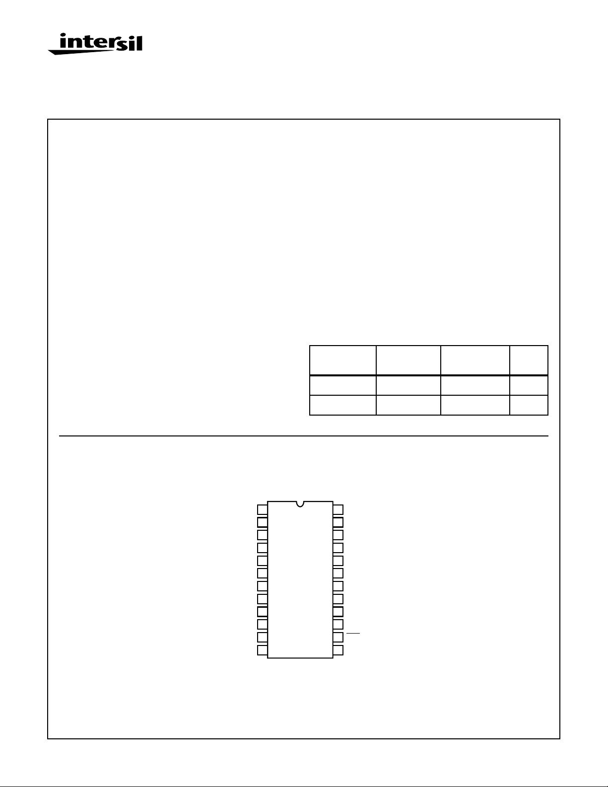
Pinout
(LSB) B1
(MSB) B8
OVERFLOW
(DIG. GND) V
(DIG. SUP.) V
B2
B3
B4
B5
B6
B7
1/4R
SS
DD
1
2
3
4
5
6
7
8
9
10
11
12
HI3318
(PDIP, SOIC)
TOP VIEW
24
VAA+ (ANA. SUP.)
3/4R
23
22
21
20
19
18
17
16
15
14
13
+
V
REF
V
IN
p
PHASE
CLK
- (ANA. GND)
V
AA
V
IN
V
-
REF
CE1
CE2
CAUTION: These devices are sensitive to electrostatic discharge; follow proper IC Handling Procedures.
1-888-INTERSIL or 321-724-7143 | Copyright © Intersil Corporation 1999
4-1452
File Number 4135.1
Page 2
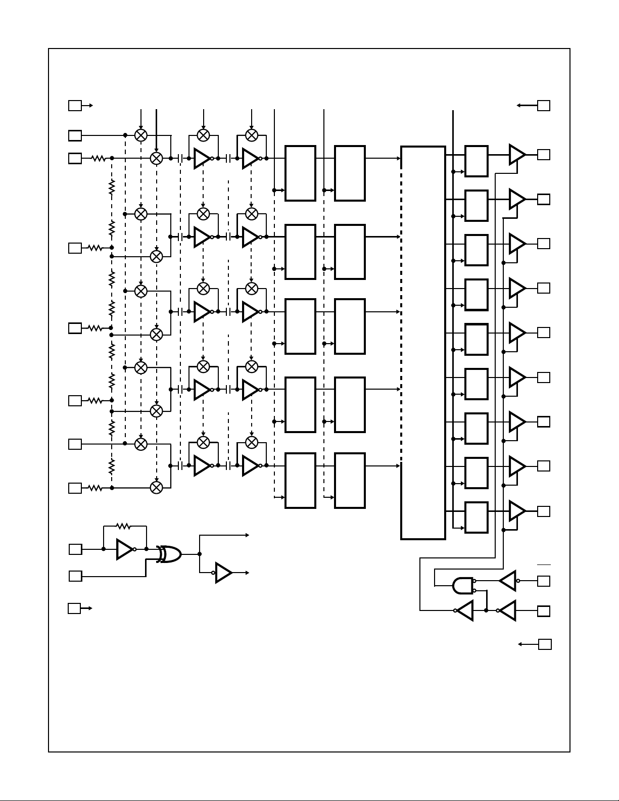
Functional Block Diagram
HI3318
VAA+
24
V
IN
21
V
REF
22
3
/4 REF
23
1
/2 REF
20
1
/4REF
10
V
IN
16
V
REF
15
CLOCK
18
PHASE
19
-
V
AA
17
+
1
/2 R
R = 2Ω
= 7Ω
= 30Ω
= 4Ω
R
≅2K
-
1
/2 R
ANALOG
SUPPLY
R
R
R
R
R
R
≅50K
ANALOG
GND
φ2 φ1 φ1 φ1 φ1 φ2 φ1
COUNT
256
COUNT
193
COUNT
129
COUNT
65
COUNT
1
ENCODER
LOGIC
ARRAY
CAB
# 256
CAB
# 193
CAB
# 129
CAB
# 65
CAB
(NOTE 1)
COMPARATOR #1
DQ
LATCH
256
DQ
LATCH
DQ
LATCH
DQ
LATCH
DQ
LATCH
1
DQ
LATCH
256
DQ
LATCH
DQ
LATCH
DQ
LATCH
DQ
LATCH
11
φ1 (AUTO BALANCE)
φ2 (SAMPLE UNKNOWN)
DIGITAL
SUPPLY
OUTPUT
REGISTER
DQ
CLK
DQ
CLK
DQ
CLK
DQ
CLK
DQ
CLK
DQ
CLK
DQ
CLK
DQ
CLK
DQ
CLK
THREE-
STATE
DRIVERS
V
DD
12
OVER-
FLOW
9
BIT 8
(MSB)
8
BIT 7
7
BIT 6
6
BIT 5
5
BIT 4
4
BIT 3
3
BIT 2
2
BIT 1
(LSB)
1
CE1
14
CE2
13
NOTE:
1. Cascaded Auto Balance (CAB).
4-1453
DIGITAL
GND
V
SS
11
Page 3
HI3318
Absolute Maximum Ratings T
DC Supply Voltage Range (VDD or VAA+) . . . . . . . . . . -0.5V to +8V
(Referenced to VSS or VAA- Terminal, Whichever is
More Negative)
Input Voltage Range
CE2 and CE1 . . . . . . . . . . . . . . . . . . . . VAA- -0.5V to VDD + 0.5V
Clock, Phase, V
Clock, Phase, V
VIN,3/4 REF, V
-,1/2 Ref. . . . . . . VAA- -0.5V to VAA+ + 0.5V
REF
-,1/4 Ref. . . . . . . . VSS- -0.5V to VDD + 0.5V
REF
+. . . . . . . . . . . . . . .VAA- -0.5V to VAA- + 7.5V
REF
=25oC Thermal Information
A
Thermal Resistance (Typical, Note 1) θJA(oC/W)
PDIP Package. . . . . . . . . . . . . . . . . . . . . . . . . . . . . 60
SOIC Package. . . . . . . . . . . . . . . . . . . . . . . . . . . . . 75
Maximum Junction Temperature. . . . . . . . . . . . . . . . . . . . . . .150oC
Maximum Storage Temperature Range . . . . . . . . . .-65oC to 150oC
Maximum Lead Temperature (Soldering 10s). . . . . . . . . . . . .300oC
(SOIC - Lead Tips Only)
Output Voltage Range, . . . . . . . . . . . . . . . VSS - 0.5V to VDD + 0.5V
Bits 1-8, Overflow (Outputs Off)
DC Input Current . . . . . . . . . . . . . . . . . . . . . . . . . . . . . . . . . ±20mA
Clock, Phase, CE1, CE2, VIN, Bits 1-8, Overflow
Recommended VAA+ Operating Range. . . . . . . . . . . . . . . VDD±1V
Recommended VAA- Operating Range . . . . . . . . . . . . . . . VSS±1V
Operating Conditions
Operating Voltage Range (VDD or VAA+). . . 4V (Min) to 7.5V (Max)
Temperature Range (TA) . . . . . . . . . . . . . . . . . . . . . . -40oC to 85oC
CAUTION: Stresses above those listed in “Absolute Maximum Ratings” may cause permanent damage to the device. This is a stress only rating and operation
of the device at these or any other conditions above those indicated in the operational sections of this specification is not implied.
NOTE:
1. θJA is measured with the component mounted on an evaluation PC board in free air.
Electrical Specifications At 25
PARAMETER TEST CONDITIONS MIN TYP MAX UNITS
SYSTEM PERFORMANCE
Resolution 8 - - Bits
Integral Linearity Error - - ± 1.5 LSB
Differential Linearity Error - - +1, -0.8 LSB
Offset Error, Unadjusted V
Gain Error, Unadjusted VIN = V
DYNAMIC CHARACTERISTICS
Maximum Input Bandwidth (Note 1) HI3318 2.5 5.0 - MHz
Maximum Conversion Speed CLK = Square Wave 15 17 - MSPS
Signal to Noise Ratio, SNR fS = 15MHz, fIN = 100kHz - 47 - dB
RMS Signal
----------------------------------
=
RMS Noise
Signal to Noise Ratio, SINAD fS = 15MHz, fIN = 100kHz - 45 - dB
RMS Signal
--------------------------------------------------------------- -
=
RMSNoise + Distortion
o
C, VAA+ = VDD = 5V, V
+ = 6.4V, V
REF
- = VAA- = VSS, CLK = 15MHz,
REF
All Reference Points Adjusted, Unless Otherwise Specified
= V
IN
- +1/2 LSB -0.5 4.5 6.4 LSB
REF
+ -1/2 LSB -1.5 0 1.5 LSB
REF
fS = 15MHz, fIN = 4MHz - 43 - dB
fS = 15MHz, fIN = 4MHz - 35 - dB
Total Harmonic Distortion, THD fS = 15MHz, fIN = 100kHz - -46 - dBc
fS = 15MHz, fIN = 4MHz - -36 - dBc
Effective Number of Bits, ENOB fS = 15MHz, fIN = 100kHz - 7.2 - Bits
fS = 15MHz, fIN = 4MHz - 5.5 - Bits
Differential Gain Error Unadjusted - 2 - %
Differential Phase Error Unadjusted - 1 - %
ANALOG INPUTS
Full Scale Range, VIN and (V
Input Capacitance, V
IN
Input Current, VIN, (See Text) VIN = 5.0V, V
REF
+) - (V
-) Notes 2, 4 4 - 7 V
REF
-30- pF
+ = 5.0V - - 3.5 mA
REF
REFERENCE INPUTS
Ladder Impedance 270 500 800 Ω
4-1454
Page 4
HI3318
Electrical Specifications At 25
o
C, VAA+ = VDD = 5V, V
+ = 6.4V, V
REF
- = VAA- = VSS, CLK = 15MHz,
REF
All Reference Points Adjusted, Unless Otherwise Specified (Continued)
PARAMETER TEST CONDITIONS MIN TYP MAX UNITS
DIGITAL INPUTS
Low Level Input Voltage, V
CE1, CE2 Note 4 - - 0.2V
Phase, CLK Note 4 - - 0.2V
High Level Input Voltage, V
CE1, CE2 Note 4 0.7V
Phase, CLK Note 4 0.7V
OL
DD
AA
IN
DD
AA
--V
--V
V
V
Input Leakage Current, II (Except CLK Input) Note 3 - ±0.2 ±5 µA
Input Capacitance, C
I
-3-pF
DIGITAL OUTPUTS
Output Low (Sink) Current VO = 0.4V 4 10 - mA
Output High (Source) Current VO = 4.5V -4 -6 - mA
Three-State Output Off-State Leakage Current, I
Output Capacitance, C
O
OZ
- ±0.2 ±5 µA
-4-pF
TIMING CHARACTERISTICS
Auto Balance Time, φ133-
∞
ns
Sample Time, φ2 Note 4 25 - 500 ns
Aperture Delay -15- ns
Aperture Jitter - 100 - ps
Data Valid Time, t
Data Hold Time, t
D
H
Output Enable Time, t
Output Disable Time, t
EN
DIS
Note 4 - 50 65 ns
Note 4 25 40 - ns
-18- ns
-18- ns
POWER SUPPLY CHARACTERISTICS
Device Current (IDD + IA) (Excludes I
) Continuous Conversion (Note 4) - 30 60 mA
REF
Auto Balance (φ1) - 30 60 mA
NOTES:
1. A full scale sine wa ve input of greater than f
/2 or the specified input bandwidth (whichever is less) ma y cause an erroneous code. The
CLK
-3dB bandwidth for frequency response purposes is greater than 30MHz.
2. VIN (Full Scale) or V
3. The clock input is a CMOS inverter with a 50kΩ feedback resistor and may be AC coupled with 1V
+ should not exceed VAA+ + 1.5V for accuracy.
REF
minimum source.
P-P
4. Parameter not tested, but guaranteed by design or characterization.
Timing Waveforms
COMPARATOR DATA IS LATCHED
CLOCK (PIN 18)
IF PHASE (PIN 19)
IS LOW
CLOCK IF
PHASE IS HIGH
DECODED DATA IS SHIFTED
TO OUTPUT REGISTERS
φ2
SAMPLE
N
DAT A
N - 2
AUTO
BALANCE
φ2 φ1φ1 φ2
SAMPLE
N + 1
DAT A
N - 1
FIGURE 1. INPUT TO OUTPUT TIMING DIAGRAM
4-1455
AUTO
BALANCE
t
H
SAMPLE
N + 2
t
D
DAT A
N
Page 5

Timing Waveforms (Continued)
CE1
CE2
t
DIS
t
EN
HI3318
t
DIS
t
EN
BITS 1 - 8
OF
DAT A
HIGH
IMPEDANCE
DAT A
DAT A DATA
HIGH
IMPEDANCE
HIGH
IMPEDANCE
FIGURE 2. OUTPUT ENABLE TIMING DIAGRAM
AUTO
BALANCE
33ns
MIN
SAMPLE
N + 1
25ns
MIN
50ns
MIN
CLOCK
DAT A
AUTO
BALANCE
NO MAX
LIMIT
SAMPLE
N
25ns
MIN
FIGURE 3A. STANDBY IN INDEFINITE AUTO BALANCE (SHOWN WITH PHASE = LOW)
CLOCK
DAT A
SAMPLE
N
500ns 33ns
MAX
BALANCE
AUTO
MIN
SAMPLE
N + 1
25ns
MIN
AUTO
BALANCE
50ns
TYP
DAT A
N - 1
SAMPLE
FIGURE 3B. STANDBY IN SAMPLE (SHOWN WITH PHASE = LOW)
FIGURE 3. PULSE MODE OPERATION
4-1456
N + 2
DAT A
N
Page 6

Typical Performance Curves
HI3318
(mA)
DD
I
40
35
30
25
20
15
10
0
fS (MHz)
302010
28
27
26
(mA)
DD
I
25
24
23
-50
-25 25 75
TEMPERATURE (oC)
FIGURE 4. DEVICE CURRENT vs SAMPLE FREQUENCY FIGURE 5. DEVICE CURRENT vs TEMPERATURE
8.0
fS = 15MHz, fI = 1MHz
7.8
7.6
7.4
7.2
7.0
6.8
ENOB (LSB)
6.6
6.4
6.2
6.0
30
40 60 8020100-10-20-30-40
TEMPERATURE (oC)
FIGURE 6. ENOB vs TEMPERATURE
907050
1.00
fS = 15MHz
0.90
0.80
0.70
0.60
0.50
0.40
0.30
NON-LINEARITY (LSB)
0.20
0.10
0
TEMPERATURE (oC)
30
40 60 8020100-10-20-30-40
FIGURE 7. NON-LINEARITY vs TEMPERATURE
INL
DNL
100500
907050
1.20
1.08
0.96
0.84
0.72
0.60
0.48
0.36
NON-LINEARITY (LSB)
0.24
0.12
0
10 200
INL
DNL
25155
fS (MHz)
1.00
fS = 15MHz
1.80
1.60
1.40
1.20
1.00
0.80
0.60
NON-LINEARITY (LSB)
0.40
0.20
0
1
INL
DNL
2460
V
(V)
REF
FIGURE 8. NON-LINEARITY vs SAMPLE FREQUENCY FIGURE 9. NON-LINEARITY vs REFERENCE VOLTAGE
4-1457
753
Page 7

Typical Performance Curves (Continued)
8.0
7.6
7.2
6.8
6.4
6.0
5.6
ENOB (BITS)
5.2
4.8
4.4
4.0
0.0 0.5 1.0 1.5 2.0 2.5 3.0 3.5 4.0 4.5
FIGURE 10. ENOB vs INPUT FREQUENCY
HI3318
fS = 15MHz
5.0
fI (MHz)
Pin Descriptions
PIN NAME DESCRIPTION
1 B1 Bit 1 (LSB) Output Data Bits
2 B2 Bit 2
3 B3 Bit 3
4 B4 Bit 4
5 B5 Bit 5
6 B6 Bit 6
7 B7 Bit 7
8 B8 Bit 8 (MSB)
9 OF Overflow
1
10
11 V
12 V
13 CE2 Three-State Output Enable Input,
14
15 V
16 V
17 V
18 CLK Clock Input
19 PHASE Sample clock phase control input.
20
21 V
22 V
23
24 V
/4 R Reference Ladder1/4 Point
SS
DD
CE1 Three-State Output Enable Input
REF
IN
AA
1
/2 R Reference Ladder Midpoint
IN
REF
3
/4 R Reference Ladder3/4 Point
AA
Digital Ground
Digital Power Supply, +5V
Active Low, See Truth Table.
Active High. See Truth Table.
- Reference Voltage Negative Input
Analog Signal Input
- Analog Ground
When PHASE is low, “Sample Unknown” occurs when the clock is low
and “Auto Balance” occurs when the
clock is high (see text).
Analog Signal Input
+ Reference Voltage Positive Input
+ Analog Power Supply, +5V
(High = True)
CHIP ENABLE TRUTH TABLE
CE1 CE2 B1 - B8 OF
0 1 Valid Valid
1 1 Three-State Valid
X 0 Three-State Three-State
X = Don’t Care
Theory of Operation
A sequential parallel technique is used by the HI3318 converter to obtain its high speed operation. The sequence consists of the “Auto-Balance” phase, φ1, and the “Sample
Unknown” phase, φ2. (Refer to the circuit diagram.) Each conversion takes one clock cycle(see Note). With the phase control (pin 19) high, the “Auto-Balance” (φ1) occurs during the
high period of the clock cycle, and the “Sample Unknown” (φ2)
occurs during the low period of the clock cycle.
NOTE: The device requires only a single phase clock The terminology of φ1 andφ2 ref ers to the high and low periods of the same clock.
During the “Auto-Balance” phase, a transmission switch is
used to connect each of the first set of 256 commutating
capacitors to their associated ladder reference tap. Those
tap voltages will be as follows:
V
(N) = [(N/256) V
TAP
= [(2N - 1)/512] V
Where:
(n) = reference ladder tap voltage at point n,
V
TAP
V
= voltage across V
REF
N = tap number (1 through 256).
The other side of these capacitors are connected to singlestage amplifiers whose outputs are shorted to their inputs by
switches. This balances the amplifiers at their intrinsic trip
points, which is approximately (V
of capacitors now charges to their associated tap voltages.
At the same time a second set of commutating capacitors and
amplifiers is also auto-balanced. The balancing of the second-
] - (1/512) V
REF
REF
]
REF
,
REF
- to V
AA
+,
REF
+ - VAA-)/2. The first set
4-1458
Page 8

HI3318
stage amplifier at its intrinsic trip point removes any tracking
differences between the first and second amplifier stages. The
cascaded auto-balance (CAB) technique, used here,
increases comparator sensitivity and temperature tracking.
In the “Sample Unknown” phase, all ladder tap switches and
comparator shorting switches are opened. At the same time
V
is switched to the first set of commutating capacitors. Since
lN
the other end of the capacitors are now looking into an effectively open circuit, any input voltage that differs from the previous tap voltage will appear as a voltage shift at the comparator
amplifiers. All comparators that had tap voltages greater than
V
will go to a “high” state at their outputs. All comparators that
lN
had tap voltages lower than V
will go to a “low” state.
lN
The status of all these comparator amplifiers is AC coupled
through the second-stage comparator and stored at the end
of this phase (φ2) by a latching amplifier stage. The latch
feeds a second latching stage, triggered at the end of φ1.
This delay allows comparators extra settling time. The status
of the comparators is decoded by a 256 to 9-bit decoder
array, and the results are clocked into a storage register at
the end of the next φ2.
A 3-stage buffer is used at the output of the 9 storage
registers which are controlled by two chip-enable signals.
CE1 will independently disable B1 through B6 when it is in a
high state. CE2 will independently disable B1 through B8
and the OF buffers when it is in the low state.
To facilitate usage of this device, a phase control input is
provided which can effectively complement the clock as it
enters the chip.
Continuous-Clock Operation
One complete conversion cycle can be traced through the
HI3318 via the following steps. (Refer to timing diagram.) With
the phase control in a “low” state, the rising edge of the clock
input will start a “sample” phase. During this entire “high” state
of the clock, the comparators will track the input v oltage and the
first-stage latches will track the comparator outputs. At the falling edge of the clock, all 256 comparator outputs are captured
by the 256 latches. This ends the “sample” phase and starts the
“auto-balance” phase for the comparators. During this “low”
state of the clock, the output of the latches settles and is captured by a second row of latches when the clock returns high.
The second-stage latch output propagates through the decode
array, and a 9-bit code appears at the D inputs of the output
registers. On the next f alling edge of the cloc k, this 9-bit code is
shifted into the output registers and appears with time delay t
as valid data at the output of the three-state drivers. This also
marks the end of the next “sample” phase, thereby repeating
the conversion process f or this ne xt cycle .
Pulse-Mode Operation
The HI3318 needs two of the same polarity clock edges to
complete a conversion cycle: If, for instance, a negative
going clock edge ends sample “N”, then data “N” will appear
after the next negative going edge. Because of this requirement, and because there is a maximum sample time of
500ns (due to capacitor droop), most pulse or intermittent
sample applications will require double clock pulsing.
If an indefinite standby state is desired, standby should be in
auto-balance, and the operation would be as in Figure 3A.
If the standby state is known to last less than 500ns and lowest average power is desired, then operation could be as in
Figure 3B.
Increased Accuracy
In most cases the accuracy of the HI3318 should be sufficient without any adjustments. In applications where accuracy is of utmost importance, five adjustments can be made
to obtain better accuracy, i.e., offset trim; gain trim; and
1
/2 and3/4 point trim.
Offset Trim
In general, offset correction can be done in the preamp circuitry by introducing a dc shift to V
the op amp. When this is not possible the V
be adjusted to produce an offset trim. The theoretical input
voltage to produce the first transition is
or by the offset trim of
lN
1
/2 LSB. The equa-
- input can
REF
tion is as follows:
(0 to 1 transition) =1/2 LSB =1/2 (V
V
lN
for the first transition is less than the theoretical, then a
If V
lN
= V
REF
/512.
single-turn 50Ω pot connected between V
will accomplish the adjustment. Set V
/256)
REF
- and ground
REF
to1/2 LSB and trim
lN
the pot until the 0-to-1 transition occurs.
for the first transition is greater than the theoretical,
If V
lN
then the 50Ω pot should be connected between V
REF
negative voltage of about 2 LSBs. The trim procedure is as
stated previously.
Gain Trim
In general, the gain trim can also be done in the preamp
circuitry by introducing a gain adjustment for the op amp.
When this is not possible, then a gain adjustment circuit
should be made to adjust the reference voltage. To perform
this trim, V
That voltage is
should be set to the 255 to overflow transition.
lN
1
/3 LSB less than V
+ and is calculated as
REF
follows:
VlN (255 to 256 transition) = V
= V
REF
REF
- V
/512
REF
(511/512).
To perform the gain trim, first do the offset trim and then
apply the required V
adjust V
+10V TO 30V
D
NOTE: Bypass V
cap. Parts noted should have low temperature drift.
FIGURE 11. TYPICAL VOLTAGE REFERENCE SOURCE FOR
+ until that transition occurs on the outputs.
REF
INPUT
CA3085E
DRIVING V
for the 255 to overflow transition. Now
lN
+
3
2
1
6
7
4
10µF, TAN
+ to analog GND near A/D with 0.1µF ceramic
REF
+ INPUT
REF
8
(NOTE 1)
5K
IOT
18Ω
CW
(NOTE 1)
1.5K
+
- and a
V
REF
(PIN 22)
4.7µF,
TAN/IOV
1
/4,
+
4-1459
Page 9

HI3318
1
/4 Point Trims
1
/4,1/2 and3/4 points on the reference ladder are
The
brought out for linearity adjusting or if the user wishes to
create a nonlinear transfer function. The
driven by the reference drivers shown (Figure 12) or by 2-K
pots connected between V
REF
+ and V
point should be set first by applying an input of 257/512 x
(V
) and adjusting for an output changing from 128 to
REF
129. Similarly the
129/512 and 385/512 x (V
192 to 193 and 64 to 65. (Note that the points are actually
1
/4,1/2 and3/4 of full scale +1 LSB.)
V
+
REF
(PIN 22)
1
/4 and3/4points can be set with inputs of
) and adjusting for counts of
REF
510Ω
510Ω
1K
POT
1K
POT
1K
POT
CW
CW
CW
4
11
3
+
2
-
5
+
6
-
10
+
9
-
+10V TO +30V
1
/4 points can be
-. The1/2 (mid-)
REF
10Ω
1
10Ω
7
10Ω
8
3
/4 REF
(PIN 23)
1
/2 REF
(PIN 20)
1
/4 REF
(PIN 10)
supply should be bypassed at the A/D to the analog side of
the ground. See Figure 15 for a block diagram of this concept. All capacitors shown should be low impedance 0.1µF
ceramics and should be mounted as close to the A/D as possible. If V
+ is derived from VDD, a small (10Ω resistor or
AA
inductor and additional filtering (4.7µF tantalum) may be
used to keep digital noise out of the analog system.
Input Loading
The HI3318 outputs a current pulse to the V
terminal at the
lN
start of every sample period. This is due to capacitor charging and switch feedthrough and varies with input voltage and
sampling rate. The signal source must be capable of recovering from the pulse before the end of the sample period to
guarantee a valid signal for the A/D to convert. Suitable high
speed amplifiers include the HA-5033, HA-2542; and
CA3450. Figure 16 is an example of an amplifier which
recovers fast enough for sampling at 15MHz.
Output Loading
The CMOS digital output stage, although capable of driving
large loads, will reflect these loads into the local ground. It is
recommended that a local QMOS buffer such as
CD74HC541 E be used to isolate capacitive loads.
NOTES:
1. All Op Amps =3/4 CA324E.
2. Bypass all reference points to analog ground near A/D with 0.1µF
ceramic caps.
3. Adjust V
FIGURE 12. TYPICAL1/4 POINT DRIVERS FOR ADJUSTING
first, then1/3,3/4 and1/4 points.
REF+
LINEARITY (USE FOR MAXIMUM LINEARITY)
9-Bit Resolution
To obtain 9-bit resolution, two HI3318s can be wired together.
Necessary ingredients include an open-ended ladder network, an overflow indicator, three-state outputs, and chipenable controls, all of which are av ailable on the HI3318.
The first step for connecting a 9-bit circuit is to totem-pole
the ladder networks, as illustrated in Figure 13. Since the
absolute resistance value of each ladder may var y, external
trim of the mid-reference voltage may be required.
The overflow output of the lower device now becomes the
ninth bit. When it goes high, all counts must come from the
upper device. When it goes low, all counts must come from
the lower device. This is done simply by connecting the lower
overflow signal to the CE1 control of the lower A/D converter
and the CE2 control of the upper A/D converter. The threestate outputs of the two devices (bits 1 through 8) are now
connected in parallel to complete the circuitry. The complete
circuit for a 9-bit A/D conv erter is shown in Figure 14.
Grounding/Bypassing
The analog and digital supply grounds of a system should be
kept separate and only connected at the A/D. This keeps
digital ground noise out of the analog data to be converted.
Reference drivers, input amps, reference taps, and the V
AA
Definitions
Dynamic Performance Definitions
Fast Fourier Transform (FFT) techniques are used to evaluate
the dynamic performance of the converter. A low distortion sine
wave is applied to the input, it is sampled, and the output is
stored in RAM. The data is then transformed into the frequency
domain with a 4096 point FFT and analyzed to evaluate the
dynamic performance of the A/D. The sine wave input to the
part is -0.5dB down from full scale for all these tests.
Signal-to-Noise (SNR)
SNR is the measured RMS signal to RMS noise at a specified input and sampling frequency. The noise is the RMS
sum of all of the spectral components except the fundamental and the first five harmonics.
Signal-to-Noise + Distortion Ratio (SINAD)
SINAD is the measured RMS signal to RMS sum of all
other spectral components below the Nyquist frequency
excluding DC.
Effective Number of Bits (ENOB)
The effective number of bits (ENOB) is derived from the
SINAD data. ENOB is calculated from:
ENOB = (SINAD - 1.76 + V
where: V
CORR
= 0.5dB.
Total Harmonic Distortion (THD)
THD is the ratio of the RMS sum of the first 5 harmonic components to the RMS value of the measured input signal.
CORR
)/6.02,
4-1460
Page 10

HI3318
6.4V REF
A
+6.4V REF
+5V
V
IN1
0V TO 6.4V
MID-POINT
DRIVER
+5V
V
+
REF
+
V
AA
-
V
AA
OF
V
DD
BIT 8
NC
+5V
A
V
IN
V
IN
BIT 1
CL
PH
CE2
CE1
V
REF
V
REF
V
-
+
SS
V
DD
D
+5V
CE2
V
IN
V
IN
VAA+
-
V
AA
V
A
REF
A
CE1
OF
BIT 8
BIT 1
CL
PH
-
V
SS
D
BIT 9
BIT 8
BIT 1
CLOCK
PHASE
+4V TO +6.5V
REFERENCE
CLOCK
SOURCE
INPUT SIGNAL
FIGURE 13. USING TWO HI3318s FOR 9-BIT RESOLUTION
4.7µF/10V TANTALUM
A
OPTIONAL CAP
(SEE TEXT)
0.01µF
AMPLIFIER/BUFFER
(SEE TEXT)
+
AD
+5V (ANALOG SUPPLY)
V
+
AA
3/4 REF
V
+
REF
V
IN
1/2 REF
PHASE
CLK
V
-
AA
V
IN
V
-
REF
CE1
CE2
BIT 1
BIT 2
BIT 3
BIT 4
BIT 5
BIT 6
BIT 7
BIT 8
OVF
1/4 REF
V
SS
V
DD
HI3318
DIGITAL
OUTPUT
D
+
4.7µF
TANTALUM/10V
A
+5V (DIGITAL SUPPLY)
FIGURE 14. TYPICAL CIRCUIT CONFIGURATION FOR THE HI3318 WITH NO LINEARITY ADJUST
4-1461
Page 11

SIGNAL
SOURCE
SIGNAL
GROUND
HI3318
V
AMP
REF
-
ANALOG
SUPPLIES
+
V
AA
SUPPLY
FIGURE 15. TYPICAL SYSTEM GROUNDING/BYPASSING
IN
IN
REF
AA
REF
V
+
+
AA
DRIVERS
-
-
OUTPUT
V
V
REFERENCE
TAPS
V
V
V
DD
V
SS
TO
DIGITAL
SYSTEM
V
DD
SUPPLY
SYSTEM
DIGITAL
GROUND
75Ω
1V
P-P
VIDEO
INPUT
75Ω
5pF
14
11
CA3450
9
3
5
4
-4V
NOTE: Ground-planing and tight layout are extremely important.
FIGURE 16. TYPICAL HIGH BANDWIDTH AMPLIFIER FOR DRIVING THE HI3318
10Ω
7
8
13
12
+8V
0.001µF
6
0.001µF
75010Ω
0.1
10Ω
390Ω
110Ω
16
A/D FLASH
INPUT
21
0V TO -10V
OFFSET SOURCE
< 10Ω
R
S
4-1462
Page 12

HI3318
TABLE 1. OUTPUT CODE TABLE
(NOTE 1)
INPUT VOLTAGE BINARY OUTPUT CODE
CODE
DESCRIPTION
Zero 0.00 0.00 000000000 0
1 LSB 0.025 0.02 000000001 1
2 LSB 0.05 0.04 000000010 2
•
•
•
1
/4 Full Scale 1.60 1.28 001000000 64
•
•
•
1
/2 Full Scale - 1 LSB 3.175 2.54 001111111 127
1
/2 Full Scale 3.20 2.56 010000000 128
1
/2 Full Scale + 1 LSB 3.225 2.58 010000001 129
•
•
•
3
/4 Full Scale 4.80 3.84 011000000 192
V
REF
6.40V (V)
•
•
•
•
•
•
•
•
•
V
REF
5.12V (V) OF
•
•
•
•
•
•
•
•
•
MSB
B8 B7 B6 B5 B4 B3 B2
•
•
•
•
•
•
•
•
•
LSB
B1
DECIMAL
COUNT
•
•
•
•
•
•
•
•
•
•
•
•
Full Scale - 1 LSB 6.35 5.08 011111110 254
Full Scale 6.375 5.10 011111111 255
Over Flow 6.40 5.12 111111111 511
NOTE: 1. The voltages listed above are the ideal centers of each output code shown as a function of its associated reference voltage.
Reducing Power
Most power is consumed while in the auto-balance state.
When operating at lower than 15MHz clock speed, power
can be reduced by stretching the sample (φ2) time. The constraints are a minimum balance time (φ1) of 33ns, and a
maximum sample time of 500ns. Longer sample times cause
droop in the auto-balance capacitors. Power can also be
•
•
•
•
•
•
•
•
•
•
•
•
Clock Input
The Clock and Phase inputs feed buffers referenced to V
and V
-. Phase should be tied to one of these two poten-
AA
AA
tials, while the clock (if DC coupled) should be driven at least
from 0.2 to 0.7 x (V
coupled with at least a 1V
levels or 5V QMOS levels when V
+ - VAA-). The clock may also be AC
AA
swing. This allows TTL drive
P-P
+ is greater than 5V.
AA
reduced in the reference string by switching the reference on
only during auto-balance.
All Intersil semiconductor products are manufactured, assembled and tested under ISO9000 quality systems certification.
Intersil products are sold by description only. Intersil Corporation reser ves the right to make changes in circuit design and/or specifications at any time without
notice. Accordingly, the reader is cautioned to verify that data sheets are current before placing orders. Information furnished by Intersil is believed to be accurate
and reliable. However, no responsibility is assumed by Intersil or its subsidiaries for its use; nor for any infringements of patents or other rights of third parties which
may result from its use. No license is granted by implication or otherwise under an y patent or patent rights of Intersil or its subsidiaries.
For information regarding Intersil Corporation and its products, see web site http://www.intersil.com
+
4-1463
 Loading...