

Page 1
HI3086
August 1997
Features
• Differential Linearity Error. . . . . . . . . . . . . . . . . ±0.2 LSB
• Integral Linearity Error . . . . . . . . . . . . . . . . . . ±0.2 LSB
• Single +5V Power Supply Operation Available
• Low Input Capacitance . . . . . . . . . . . . . . . . . . . . . . . 7pF
• Wide Analog Input Bandwidth . . . . . . . . . . . . . 200MHz
• Low Power Consumption . . . . . . . . . . . . . . . . . .360mW
• CLK/2 Clock Output Pin
• Excellent Temperature Characteristics
• 1:2 Demultiplexed Output
1
• Internal
/2 Frequency Divider Circuit
(With Reset Function)
• Compatible with ECL, PECL and TTL Digital Input Levels
• Direct Replacement for Sony CXA3086
Applications
• RGB Graphics Processing (LCD, PDP)
• Digital Communications (QPSK, QAM)
• Magnetic Recording (PRML)
6-Bit, 140 MSPS, Flash A/D Converter
Description
The HI3086 is a 6-bit, high-speed, flash analog-to-digital converter optimized for high speed, low power, and ease of use.
With a 140 MSPS encode rate capability and full-power analog
bandwidth of 200MHz, this component is ideal for applications
requiring the highest possible dynamic performance.
To minimize system cost and power dissipation, only a +5V
power supply is required. The HI3086’s clock input interfaces
directly to TTL, ECL, or PECL logic and will operate with singleended inputs. The user may select 16-bit demultiplexed output
or 8-bit single-channel digital outputs. The demultiplexed mode
interleaves the data through two 8-bit channels at
rate. Operation in demultiplexed mode reduces the speed and
cost of external digital interfaces, while allowing the A/D
converter to be clocked to the full 140 MSPS conv ersion r ate .
Fabricated with an advanced bipolar process, the HI3086 is
provided in a space-saving 48-lead MQFP surface mount
plastic package and is specified over the -20
temperature range.
Ordering Information
PART
NUMBER
HI3086JCQ -20 to 75 48 Ld MQFP Q48.12x12-S
HI3086EVAL 25 Evaluation Board
TEMP.
RANGE (oC) PACKAGE PKG. NO.
1
/2 the clock
o
C to 75oC
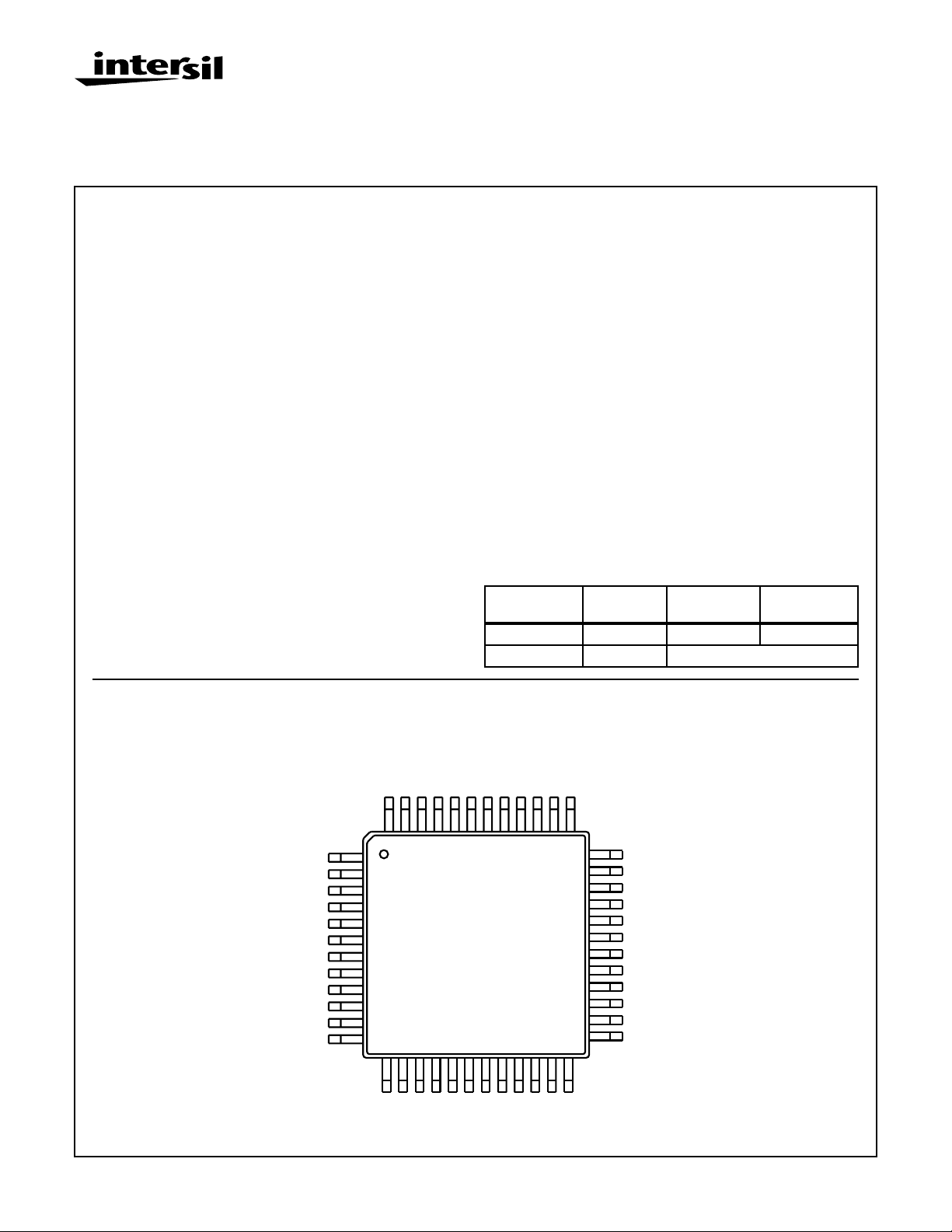
Pinout
DGND2
P2D0 (LSB)
P2D1
P2D2
P2D3
P2D4
P2D5 (MSB)
DGND2
DV
CC2
RESETN/T
RESET/E
RESETN/E
CC2
DV
DV
1
2
3
4
5
6
7
8
9
10
11
12
13 14 15 16
EE3
AGND
DV
HI3086 (MQFP)
TOP VIEW
CC1
DGND1
PS
NC
CC
RB
RBS
V
V
AV
CLKOUT
NC
INV
IN
V
NC
SELECT
RT
CC
V
AV
CC1
DV
DGND1
RTS
V
AGND
CC2
DV
373839404142434445464748
36
35
34
33
32
31
30
29
28
27
26
25
2423222120191817
DGND3
DGND2
P1D5 (MSB)
P1D4
P1D3
P1D2
P1D1
P1D0 (LSB)
DGND2
DV
CC2
CLK/T
CLKN/E
CLK/E
CAUTION: These devices are sensitive to electrostatic discharge; follow proper IC Handling Procedures.
1-888-INTERSIL or 321-724-7143 | Copyright © Intersil Corporation 1999
4-1406
File Number 4110.1
Page 2
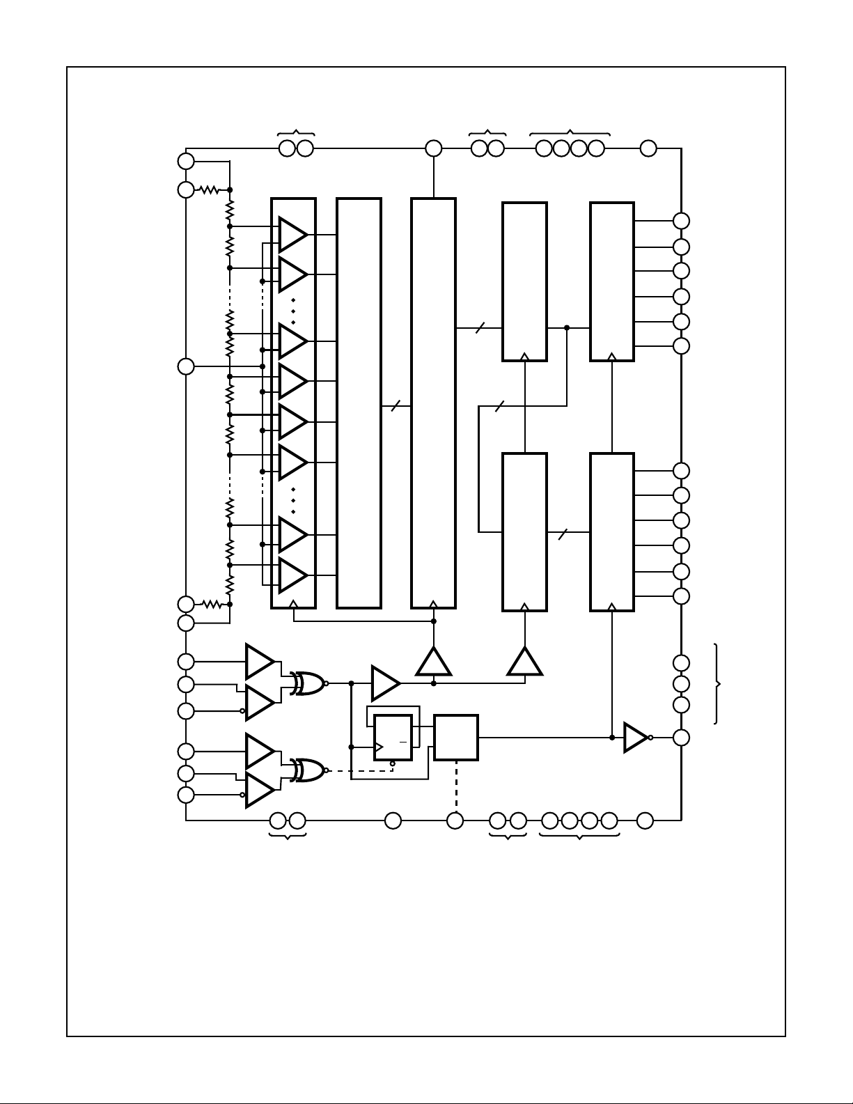
Functional Block Diagram
HI3086
V
V
RTS
V
V
V
RB
RBS
RT
AV
CC
22
R1
21
19
IN
16
15
R2
R
R
R
R
R
R
R
R
R
17 20 42 38 9 28 37 24
1
2
30
31
32
33
62
63
6-BIT
ENCODER
6-BIT LATCH
DV
CC1
47 48
6-BIT
6-BIT
LATCH B LATCH A
DV
CC2
6-BIT
DGND3INV
TTLOUT
TTLOUT
(MSB)
35
P1D5
34
P1D4
33
P1D3
32
P1D2
31
P1D1
30
P1D0
(LSB)
(MSB)
P2D5
7
6
P2D4
P2D3
5
P2D2
4
P2D1
3
P2D0
2
(LSB)
CLK/T
CLK/E
RESETN/T
RESETN/E
RESET/E
27
25
26CLKN/E
10
12
11
14 23 8 29 36 13141 463944
DELAY
DQ
18
40
45
SELECT
Q
DGND2DGND1AGND PS SELECT
DV
43NCCLKOUT
EE3
4-1407
Page 3
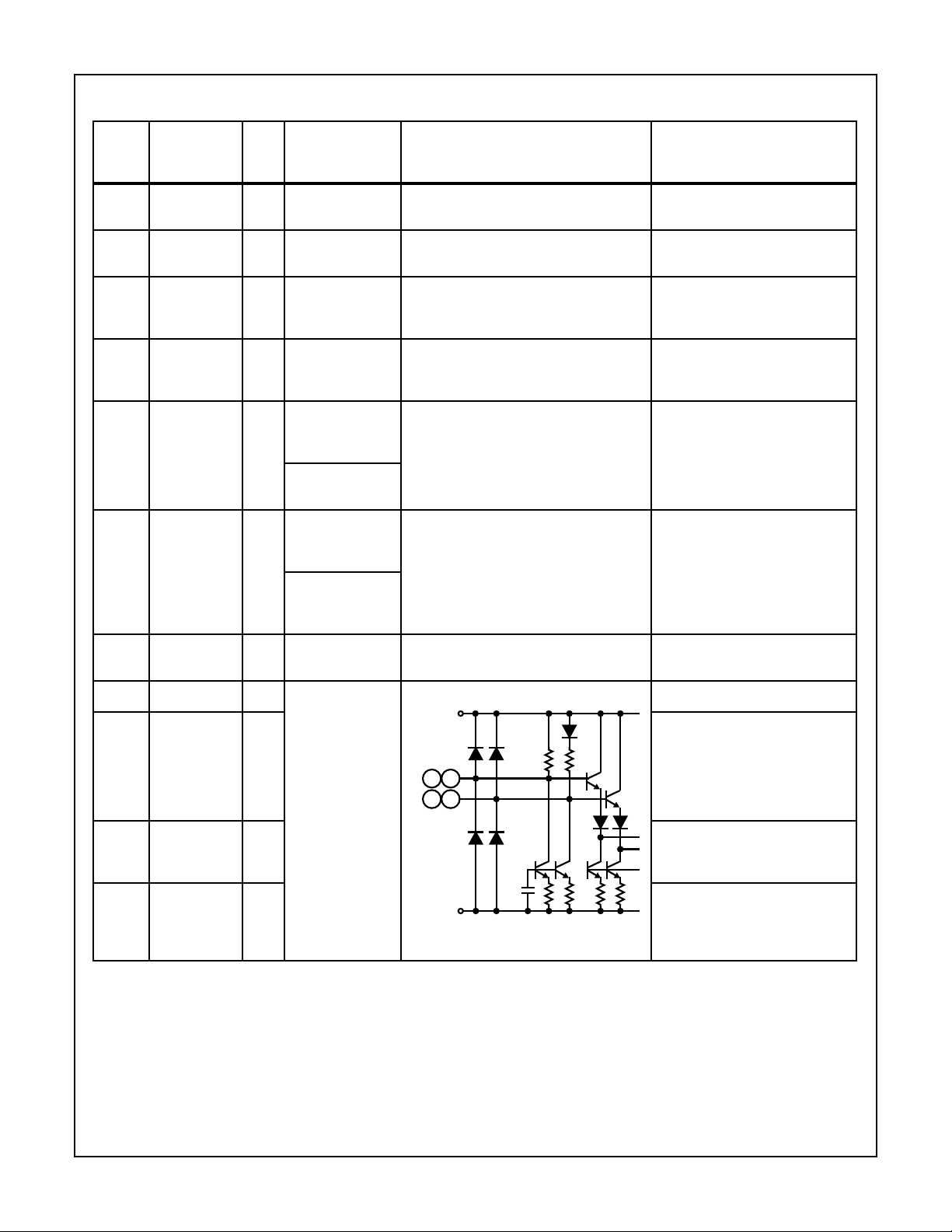
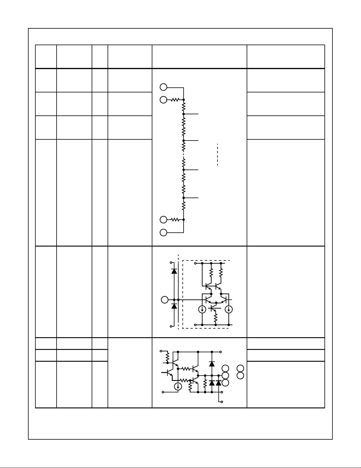
HI3086
Pin Descriptions
TYPICAL
PIN
NO. SYMBOL I/O
14, 23 AGND GND Analog Ground. Separated from
VOLTAGE
LEVEL EQUIVALENT CIRCUIT DESCRIPTION
the digital ground.
17, 20 AV
CC
+5V (Typ) Analog Power Supply. Separated
from the digital power supply.
1, 8, 29,
36, 39,
DGND1
DGND2
GND Digital Ground.
46
9, 28,
37, 38,
DV
DV
CC1
CC2
+5V (Typ) Digital Power Supply.
47, 48
24
DGND3
+5V (Typ) (With a
Single Power
Supply)
Digital Power Supply. Ground for
ECL input. +5V for PECL and TTL
input.
GND (With Dual
Power Supplies)
13
D
VEE3
GND (With a
Single Power
Supply)
Digital Power Supply. Ground for
ECL input. -5V for PECL and TTL
input.
-5V (Typ) (With
Dual Power
Supplies)
18, 40,
45
NC No Connect pin. Not connected
with the internal circuits.
25 CLK/E I ECL/PECL Clock input.
26
I CLK/E Complementary Input. When
DGND3
left open, this pin goes to the thresh-
CLKN/E
RR
12 25
2611
old potential. Only CLK/E can be
used for operation, but complementary input is recommended to attain
fast and stable operation.
12
11
RESETN/E
RESET/E
I Reset Input. When the input is set to
low level, the built-in CLK frequency
divider circuit can be reset.
1.2V
I RESETN/E Complementary Input.
DV
EE3
RR
When left open, this pin goes to the
threshold voltage. Only RESETN/E
can be used for operation.
4-1408
Page 4
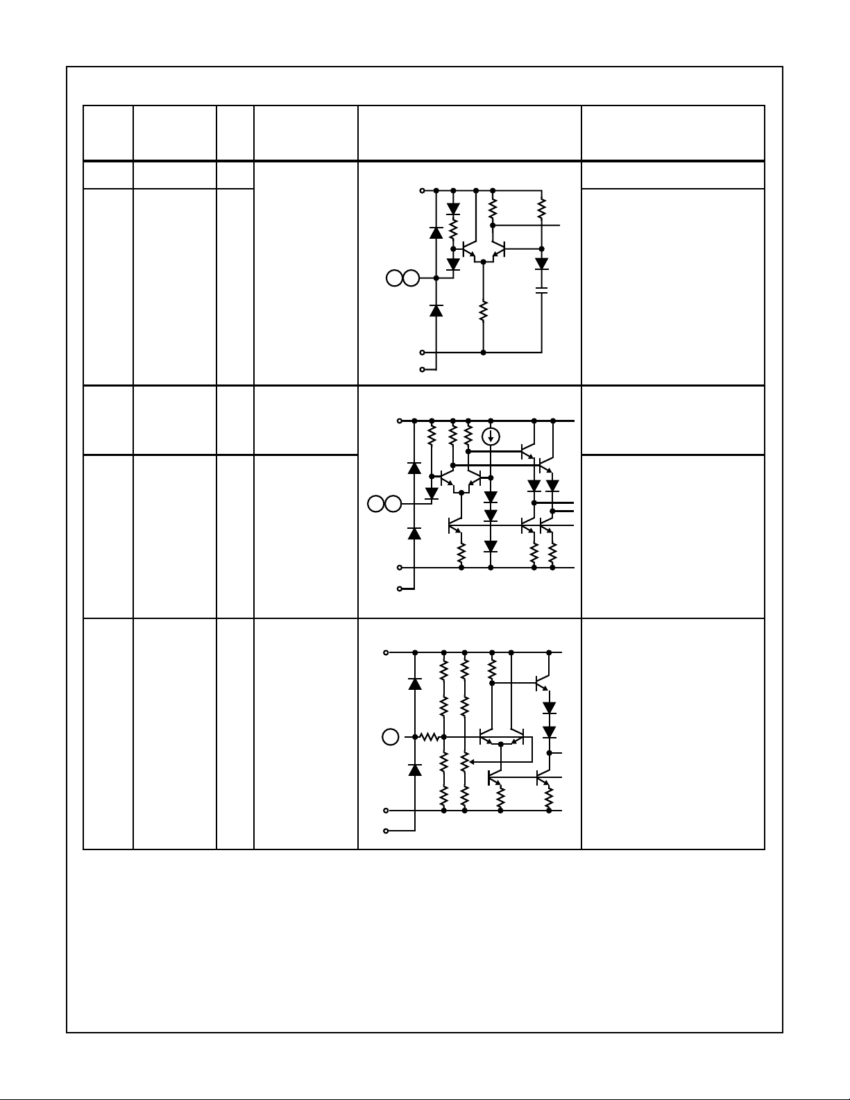
Pin Descriptions (Continued)
PIN
NO. SYMBOL I/O
HI3086
TYPICAL
VOLTAGE
LEVEL EQUIVALENT CIRCUIT DESCRIPTION
27 CLK/T I TTL Clock Input.
10 RESETN/T I Reset Input. When left open, this
D
VCC1
R/2
input goes to high level. When the
input is set to low level, the built-in
CLK frequency divider circuit can
be reset.
2710
DGND1
DV
EE3
42 INV I TTL Data Output Polarity Inversion Input.
D
VCC1
1.5V
R
When left open, this input goes to
high level. (See Table 1; I/O
Correspondence Table).
44 PS I TTL Power Saving Input. When the input
is set to low level, the power saving
44
42
mode is set. In this time the all TTL
ouputs go into the high impedance
state. Normally, set to high level or
left open.
DGND1
D
VEE3
41 SELECT V
or GND Data Output Mode Selection. (See
CC
D
VCC1
41
DGND1
D
VEE3
Table 2, Operating Mode Table).
4-1409
Page 5
Pin Descriptions (Continued)
PIN
NO. SYMBOL I/O
HI3086
TYPICAL
VOLTAGE
LEVEL EQUIVALENT CIRCUIT DESCRIPTION
22 V
21 V
16 V
15 V
RTS
RT
RB
RBS
O +4.0V (Typ) Reference Voltage Sense. Bypass
to AGND with a 0.1µF chip
22
IV
IV
RTS
RBS
+ R1 x I
-R2 x I
REF
REF
O +2.0V (Typ) Reference Voltage Sense. Bypass
R1
21
R
COMPARATOR 1
R
R
COMPARATOR 2
R
capacitor.
Top Reference Voltage. Bypass to
AGND with a 1µF tantal capacitor
and 0.1µF chip capacitor.
Bottom Reference Voltage. Bypass
to AGND with a 1µF tantal capacitor
and a 0.1µF chip capacitor.
to AGND with a 0.1µF chip
capacitor.
R
COMPARATOR 62
R
R
COMPARATOR 63
R
R2
16
15
19 V
IN
30 to 35 P1D0 to P1D5 O TTL Port 1 Side Data Output.
2 to 7 P2D0 to P2D5 O Port 2 Side Data Output.
43 CLKOUT O Clock Output. (See Table 2.
IVRT to V
RB
AV
CC
19
DV
EE3
DV
CC1
DGND1
COMPARATOR
AV
CC
AGND
100K
DV
CC2
2
TO
304335
TO
DGND2
DV
EE3
Analog Input.
V
REF
7
Operating Mode Table.)
4-1410
Page 6
HI3086
Absolute Maximum Ratings (T
Supply Voltage . . . . . . . . . . . (AVCC, DV
(DGND3). . . . . . . . . . . . . . . . . . . . . . . . . . . . . . . . . . -0.5V to 7.0V
(DV
). . . . . . . . . . . . . . . . . . . . . . . . . . . . . . . . . . . -7.0V to 0.5V
EE3
(DGND3 - DV
Analog Input Voltage (VIN) . . . . . . . . . . . . . . . . .VRT - 2.7V to AV
Reference Input Voltage (VRT). . . . . . . . . . . . . . . . . . .2.7V to AV
(VRB). . . . . . . . . . . . . . . . . . . . . . . . . . . . . . . . VIN - 2.7V to AV
). . . . . . . . . . . . . . . . . . . . . . . . . . . -0.5V to 7.0V
EE3
=25oC) Thermal Information
A
, DV
CC1
) -0.5V to 7.0V
CC2
Thermal Resistance (Typical, Note 1) θJA (oC/W)
MQFP Package. . . . . . . . . . . . . . . . . . . . . . . . . . . . 63
Maximum Junction Temperature (Plastic Package) . . . . . . . . 150oC
Maximum Storage Temperature Range . . . . . . . . . .-65oC to 150oC
CC
Maximum Lead Temperature (Soldering 10s) . . . . . . . . . . . . . 300oC
CC
CC
(MQFP - Lead Tips Only)
(|VRT - VRB|). . . . . . . . . . . . . . . . . . . . . . . . . . . . . . . . . . . . . .2.5V
Digital Input Voltage
ECL (***/E (Note 2)) . . . . . . . . . . . . . . . . . . . . . . . .DV
EE3
to 0.5V
PECL (***/E) . . . . . . . . . . . . . . . . . . . . . . . . . . . . -0.5V to DGND3
TTL (***/T, INV PS) . . . . . . . . . . . . . . . . . . . . . . . . -0.5V to DV
Other (SELECT) . . . . . . . . . . . . . . . . . . . . . . . . . . -0.5V to DV
CC1
CC1
VID (|***/E - ***N/E| (Note 3)) . . . . . . . . . . . . . . . . . . . . . . . . .2.7V
Recommended Operating Conditions
WITH A SINGLE POWER SUPPLY MIN TYP MAX
Supply Voltage
DV
CC1
, DV
, AVCC . . . . . . . . . +4.75 +5.0 +5.25V
CC2
DGND1, DGND2, AGND . . . . . . . -0.05 0 +0.05V
DGND3 . . . . . . . . . . . . . . . . . . . . . +4.75 +5.0 +5.25V
DV
. . . . . . . . . . . . . . . . . . . . . . -0.05 0 +0.05V
EE3
Analog Input Voltage (VIN) . . . . . . . . V
RB
-V
Reference Input Voltage
VRT. . . . . . . . . . . . . . . . . . . . . . . . +2.9 - +4.1V
VRB. . . . . . . . . . . . . . . . . . . . . . . . 1.4 - +2.6V
|VRT - VRB|. . . . . . . . . . . . . . . . . . 1.5 - 2.1V
Digital Input Voltage
ECL (***/E) VIH. . . . . . . . . . . . . . . . DGND3 - 1.05 DGND3 - 0.5V
PECL (***/E) VIL DGND3 . . . . . . . DGND3 - 3.2 DGND3 - 1.4V
TTL (***/T, INV, PS) VIH . . . . . . . . 2.0V - -
TTL (***/T, INV) VIL. . . . . . . . . . . . - - 0.8V
Other (SELECT) VIH. . . . . . . . . . . - DV
CC1
Other (SELECT) VIL. . . . . . . . . . . - DGND1 -
VID (Note 3) (|***/E- ***N/E|). . . . . 0.4 0.8 -
Max Conversion Rate (fC, Straight Mode) . . . 100 - -
Units = MSPS
Max Conversion Rate (fC, DMUX Mode). . . . 140 - -
Units = MSPS
Ambient Temperature (TA) . . . . . . . . . . . . . . . . . . . . . -20oC to 75oC
CAUTION: Stresses above those listed in “Absolute Maximum Ratings” may cause permanent damage to the device. This is a stress only rating and operation
of the device at these or any other conditions above those indicated in the operational sections of this specification is not implied.
NOTES:
1. θJA is measured with the component mounted on an evaluation PC board in free air.
2. ***/E and ***T indicate CLK/E and CLK/T, etc. for the pin name.
3. VID: Input Voltage Differential.
WITH DUAL POWER SUPPLIES MIN TYP MAX
Supply Voltage
DV
, DV
CC1
, AVCC . . . . . . . . . +4.75 +5.0 +5.25V
CC2
DGND1, DGND2, AGND. . . . . . . . -0.05 0 +0.05V
DGND3 . . . . . . . . . . . . . . . . . . . . . -0.05 0 +0.05V
DV
. . . . . . . . . . . . . . . . . . . . . . -5.5 -5.0 -4.75V
EE3
Analog Input Voltage (VIN) . . . . . . . . V
RT
RB
Reference Input Voltage
VRT . . . . . . . . . . . . . . . . . . . . . . . . +2.9 - +4.1V
VRB . . . . . . . . . . . . . . . . . . . . . . . . 1.4 - +2.6V
|VRT - VRB| . . . . . . . . . . . . . . . . . . 1.5 - 2.1V
Digital Input Voltage
ECL (***/E) VIH DGND3 . . . . . . . .DGND3 - 1.05 DGND3 - 0.5V
ECL (***/E) VIL DGND3. . . . . . . . . DGND3 - 3.2 DGND3 -1.4V
TTL (***/T, INV) VIH. . . . . . . . . . . . . . . . . 2.0V - -
TTL (***/T, INV) VIL . . . . . . . . . . . . . . . . . - - 0.8V
-
Other (SELECT) VIH . . . . . . . . . . . . . . . . - DV
Other (SELECT) VIL . . . . . . . . . . . . . . . . - DGND1 -
VID (Note 3) (|***/E- ***N/E|) . . . . . . . . . . 0.4 0.8 -
Max Conversion Rate (fC, Straight Mode). . . 100 - -
Units = MSPS
Max Conversion Rate (fC, DMUX Mode). . . . 140 - -
Units = MSPS
Ambient Temperature (TA). . . . . . . . . . . . . . . . . . . . . .-20oC to 75oC
-V
CC1
RT
-
Electrical Specifications DV
TA = 25oC, PECL Input
PARAMETER SYMBOL TEST CONDITIONS MIN TYP MAX UNITS
Resolution
DC CHARACTERISTICS
Integral Linearity Error
Differential Linearity Error
, AVCC, DGND3 = +5V, DGND1, 2, AGND, DV
CC1,2
IL
DL
VIN = 2V
E
E
= 5 MSPS - - ±0.2 LSB
P-P,fC
4-1411
= 0V, VRT = 4V, VRB = 2V,
EE3
- 6 - Bits
--±0.2 LSB
Page 7

HI3086
Electrical Specifications DV
, AVCC, DGND3 = +5V, DGND1, 2, AGND, DV
CC1,2
= 0V, VRT = 4V, VRB = 2V,
EE3
TA = 25oC, PECL Input (Continued)
PARAMETER SYMBOL TEST CONDITIONS MIN TYP MAX UNITS
ANALOG INPUT
Analog Input Capacitance C
Analog Input Resistance R
Analog Input Current I
IN
VIN = +3.0V + 0.07V
IN
IN
RMS
-7-pF
16 - 150 kΩ
0 - 125 µA
REFERENCE INPUT
Reference Resistance (Note 5) R
Reference Current (Note 6) I
REF
REF
160 225 308 Ω
6.5 9.0 12.5 mA
Residual Resistance R1 3.0 4.2 5.7 Ω
R2 3.0 4.2 5.7 Ω
DIGITAL INPUT (ECL, PECL)
Digital Input Voltage: High V
Digital Input Voltage: Low V
Threshold Voltage V
Digital Input Current: High I
Digital Input Current: Low I
IH
IH
IL
TH
VIH = DGND3 -0.8V -50 - +50 µA
VIL = DGND3 -1.6V -75 - 0 µA
IL
DGND3 -1.05 - DGND3 -0.5 V
DGND3 -3.2 - DGND3-1.4 V
- DGND3 -1.2 - V
Digital Input Capacitance - - 5 pF
DIGITAL INPUT (TTL)
Digital Input Voltage: High V
Digital Input Voltage: Low V
Threshold Voltage V
Digital Input Current: High I
Digital Input Current: Low I
IH
IH
IL
TH
VIH = 3.5V -50 - 0 µA
VIL = 0.2V -500 - 0 µA
IL
2.0 - - V
- - 0.8 V
- 1.5 - V
Digital Input Capacitance - - 5 pF
DIGITAL OUTPUT (TTL)
Digital Output Voltage: High V
Digital Output Voltage: Low V
Leakage Current I
OH
OL
OZ
IOH = -2mA 2.4 - - V
IOL = 1mA - - 0.5 V
Power Saving Mode -15 - 70 µA
SWITCHING CHARACTERISTICS
Maximum Conversion Rate f
Aperture Jitter t
Sampling Delay t
Clock High Pulse Width t
Clock Low Pulse Width t
Reset Signal Setup t
RESET Signal Hold t
CLKOUT Output Delay t
DCLK
Data Output Delay (Note 7) t
t
Output Rise Time t
Output Fall Time t
AJ
DS
PW1
PW0
RS
RH
DO1
DO2
DMUX Mode 140 - - MSPS
C
-10-ps
3 4.5 6 ns
CLK 2.9 - - ns
CLK 2.9 - - ns
RESETN - CLK 3.5 - - ns
RESETN - CLK 0 - - ns
(CL = 5pF) 3.5 7 9 ns
DMUX Mode (CL = 5pF) t (Note 6) t + 1 t + 2 ns
(CL = 5pF) 4.5 8 10 ns
0.8V to 2.0V (CL = 5pF) - 2 - ns
r
0.8V to 2.0V (CL = 5pF) - 2 - ns
f
4-1412
Page 8

HI3086
Electrical Specifications DV
, AVCC, DGND3 = +5V, DGND1, 2, AGND, DV
CC1,2
TA = 25oC, PECL Input (Continued)
PARAMETER SYMBOL TEST CONDITIONS MIN TYP MAX UNITS
DYNAMIC CHARACTERISTICS
Input Bandwidth VIN = 2V
P-P
S/N Ratio fC = 140 MSPS,
fIN = 1kHz Full Scale,
DMUX Mode
fC = 140 MSPS,
fIN = 34.999MHz Full Scale,
DMUX Mode
Error Rate f
= 140 MSPS,
C
fIN = 1kHz Full Scale,
DMUX Mode
Error > 4 LSB
= 140 MSPS,
f
C
fIN = 34.999MHz Full Scale,
DMUX Mode
Error > 4 LSB
= 100 MSPS,
f
C
fIN = 24.999MHz Full Scale,
Straight Mode
Error > 4 LSB
POWER SUPPLY
Supply Current I
Supply Current I
Power Consumption (Note 9) P
Supply Current ICC + I
Power Consumption P
CC
EE
D
Power Saving Mode 2.0 - 8.0 mA
EE
Power Saving Mode 28.0 - 58.0 mW
D
NOTES:
4.
R
: Resistance value between VRT and VRB.
REF
VRT-V
I
5.
REF
RB
--------------------------- -=
R
REF
.
= 0V, VRT = 4V, VRB = 2V,
EE3
, -3dB 200 - - MHz
- 37.0 - dB
- 34.5 - dB
--10
-12
TPS
(Note 8)
--10-9TPS
--10-9TSP
54.0 67.5 90.0 mA
0.4 0.6 0.8 mA
290 360 470 mW
1
t
6.
-----=
.
f
C
7.
TPS: Times Per Sample
P
8. .
DICCIEE
+()VCC•
.
()
V
RT-VRB
----------------------------------- -+=
V
REF
2
4-1413
Page 9

TABLE 1. I/O CORRESPONDENCE
10
V
V
IN
RTS
STEP
D5 D0 D5 D0
63 111111000000
62 111110000001
•
•
•
•
•
•
32 100000011111
31 011111100000
•
•
•
•
•
•
1 000001111110
V
RBS
0 000000111111
HI3086
V
ID
FIGURE 1. ECL AND PECL SWITCHING LEVEL
INV
•
•
•
•
•
•
STEP
63
62
61
60
59
58
5
4
3
2
1
0
R1 x I
VRTV
REF
RTS
1 LSB
V
FIGURE 2.
DGND3
V
(MAX)
IH
V
IL
VTH (DGND3 - 1.2V)
V
IH
VIL (MIN)
IN
R2 x I
V
RBSVRB
REF
Test Circuits
5V 5V
I
A A
CC
AV
4V
1.95V
2V
V
RT
V
IN
V
RB
CC
DV
CC1
DV
CC2
DGND2
DGND1
AGND
FIGURE 3. CURRENT CONSUMPTION MEASUREMENT
CIRCUIT
DGND3
CLK/E
DV
EE3
I
EE
5MHz PECL
100MHz
OSC1
φ: VARIABLE
f
OSC2
100MHz
AMP
V
R
IN
HI3086
CLK
ECL
BUFFER
FIGURE 4. SAMPLING DELAY MEASUREMENT CIRCUIT
APERTURE JITTER MEASUREMENT CIRCUIT
4-1414
6
LOGIC
ALALYZER
1024
SAMPLES
Page 10

Test Circuits (Continued)
HI3086
+V
S2
DVM
-
+
-V
COMPARATOR
V
IN
HI3086 BUFFER
6
“0”
CONTROLLER
S1: ON WHEN A < B
S1
S2: ON WHEN A > B
A < B A > B
A6
B6
TO
TO
A1
B1
B0A0
“1”
6
00...00
TO
11..10
FIGURE 5. INTEGRAL LINEARITY ERROR MEASUREMENT
CIRCUIT DIFFERENTIAL LINEARITY ERROR MEASUREMENT CIRCUIT
SIGNAL
SOURCE
V
IN
HI3086 LATCH
6
V
RT
V
IN
V
RB
CLK
33
32
31
30
29
SAMPLING TIMING FLUCTUATION
(= APERTURE JITTER)
(LSB)
σ
V
CLK
∆ν
∆t
IN
NOTE: Where σ (LSB) is the deviation of the output codes when the
largest slew rate point is sampled at the clock which has exactly the
same frequency as the analog input signal, the aperture jitter Tai is:
tAJ= σ/
∆υ
-------
∆T
64
------
= σ/
x2πf
2
.
FIGURE 6. APERTURE JITTER MEASUREMENT METHOD
A
COMPARATOR
A > B
PULSE
COUNTER
f
C
4
2V
SINE WAVE
P-P
SIGNAL
SOURCE
-1kHz
CLK CLK
+
4 LSB
1
/
8
f
C
LATCH
B
FIGURE 7. ERROR RATE MEASUREMENT CIRCUIT
Operating Modes
The HI3086 has two types of operating modes which are selected with Pin 41 (SELECT).
TABLE 2. OPERATING MODE
OPERATING
MODE
DMUX Mode V
SELECT
CC
Straight Mode GND 100 Mbps Straight Output 100 Mbps
Demux Mode (See Figures 19, 20, 21).
Set the SELECT pin to V
for this mode. In this mode, the
CC
clock frequency is divided by 2 in the IC, and the data is output after being demultiplexed by this
clock. The
1
/2 frequency divided clock, which has adequate
setup time and hold time for the output data, is output from
the CLKOUT pin.
MAXIMUM
CONVERSION RATE
DATA OUTPUT CLOCK OUTPUT
140 Mbps Demultiplexed Output 70 Mbps
When using multiple HI3086 units in parallel in this mode, differences in the start timing of the
may cause operation as shown in Figures 8 and 9. As a coun-
1
/2 frequency divided
termeasure, the HI3086 is equipped with a function which
resets the
1
clock, the RESET pulse must be input to the RESET pin. See
the Timing Charts for the RESET pulse input timing. The A/D
converter can operate at f
/2 frequency divided clock. When resetting this
The input clock is1/2 frequency
divided and output at 70MHz.
The input clock is inverted and
output at 100MHz.
1
/2 frequency divided clock
(Min) = 140 MSPS in this mode.
C
4-1415
Page 11

CLK
HI3086
CLK
CLK
RESET PULSE
HI3086
CLK
RESETN
HI3086
CLK
RESETN
A
B
HI3086
CLK
RESETN
HI3086
CLK
RESETN
6-BITS
6-BITS
CLKOUT
DAT A
CLKOUT
DAT A
FIGURE 8. WHEN THE RESET PULSE IS NOT USED
CLK
RESET
PULSE
A
6-BITS
B
6-BITS
CLKOUT
DAT A
CLKOUT
DAT A
FIGURE 9. WHEN THE RESET PULSE IS USED
Straight Mode (See Figures 22, 23, 24 and 25).
Set the SELECT pin to GND for this mode. In this mode,
data output can be obtained in accordance with the clock frequency applied to the A/D converter for applications which
use the clock applied to the A/D converter as the system
clock.
The A/D converter can operate at f
(Min) = 100 MSPS in
C
this mode.
Digital Input Level and Supply Voltage Settings
The logic input level f or the HI3086 supports ECL, PECL and
TTL levels. The power supplies (D
, DGND3) for the
VEE3
logic input block must be set to match the logic input (CLK
and RESET signals) level.
T ABLE 3. LOGIC INPUT LEVEL AND POWER SUPPL Y SETTINGS
DIGITAL
INPUT
LEVEL D
VEE3
DGND3
ECL -5V 0V ±5V Figures 19, 22
PECL 0V +5V +5V Figures 20, 23
TTL 0V +5V +5V Figures 21, 24, 25
SUPPLY
VOLTAGE
APPLICATION
CIRCUITS
4-1416
Page 12

Timing Waveforms
HI3086
V
CLK
P1D0 TO D5
P2D0 TO D5
CLK OUT
RESET PULSE
N - 1
t
t
PW1
t
RS
RH
t
DS
t
t
t
PW0
DCLK
N
2.0V 2.0V
0.8V
N + 1
IN
N - 2
N - 3
N + 2
t
DO2
t + 1ns
0.8V
t
DO1
N + 3
2.0V
0.8V
2.0V
N - 1
0.8V
≠ t ≠ t
N
N + 2
N + 1
FIGURE 10. DEMUX MODE TIMING CHART (SELECT = VCC)
V
CLK
P1D0 TO D5
P2D0 TO D5
(CLK IS INVERTED
CLK OUT
AND OUTPUT)
RESET PULSE
N - 1
IN
t
DS
t
t
PW1tPW0
2.0V
N - 4
0.8V
2.0V
N - 5
0.8V
t
D02
2.0V
0.8V
t
DCLK
N
N - 3
N - 4
N + 1
N - 2
N - 3
N + 2
N - 1
N - 2
N + 3
N
N - 1
FIGURE 11. STRAIGHT MODE TIMING CHART (SELECT = GND)
4-1417
Page 13

Notes on Operation
HI3086
• The HI3086 is a high-speed A/D converter which is
capable of TTL, ECL and PECL level clock input. Characteristic impedance should be properly matched to ensure
optimum performance during high-speed operation.
• The power supply and grounding have a profound
influence on converter performance. The power supply
and grounding method are particularly important during
high-speed operation. General points for caution are as
follows:
- The ground pattern should be as large as possible. It is
recommended to make the power supply and ground
patterns wider at an inner layer using a multi-layer
board.
- To prevent interference between AGND and DGND and
between AV
and DVCC, make sure the respective
CC
patterns are separated. To prevent a DC offset in the
power supply pattern, connect the AV
and DV
CC
CC
lines at one point each via a ferrite-bead filter. Shorting
the AGND and DGND patterns in one place immediately under the A/D converter improves A/D conver ter
performance.
- Ground the power supply pins (AV
CC
, DV
CC1
, DV
CC2
DVEE3) as close to each pin as possible with a 0.1µF or
larger ceramic chip capacitor. (Connect the AVCC pin to
the AGND pattern and the DV
CC1
, DV
CC2
, DV
EE3
pins
to the DGND pattern.)
- The digital output wiring should be as short as possible.
If the digital output wiring is long, the wiring capacitance
will increase, deteriorating the output slew rate and
resulting in reflection to the output wavefor m since the
original output slew rate is quite fast.
• The analog input pin V
has an input capacitance of
IN
approximately 7pF. To drive the A/D converter with proper
frequency response, it is necessary to prevent performance deterioration due to parasitic capacitance or
parasitic inductance by using a large capacity drive circuit;
keeping wiring as short as possible, and using chip parts
for resistors and capacitors, etc.
• The V
and VRB pins must have adequate bypass to
RT
protect them from high-frequency noise. Bypass them to
AGND with approximately 1µF tantal capacitor and, 0.1µF
chip capacitor as short as possible.
• The offset for residual is generated each for the reference
voltage pins V
and VRB. When the offset voltage has
RT
no influence on the IC operation, the voltage should be
applied to the V
V
pin open. When the reference voltage is to be
RBS
and VRB pins directly, keeping the
RT
supplied to these pins precisely, form the feedback loop
circuit with V
and VRB as a force pin and adjust the
RT
offset voltage to be 0V. See Figure 25 for details.
• If the CLKN/E pin is not used, bypass this pin to DGND
with an approximately 0.1µF capacitor. At this time,
,
approximately DGND3 -1.2V voltage is generated. However, this is not recommended for use as threshold voltage
V
as it is too weak.
BB
• When the digital input level is ECL or PECL level, ***/E
pins should be used and ***/T pins left open. When the
digital input level is TTL, ***/T pins should be used and
***/E pins left open.
Typical Performance Curves
70
65
60
55
CURRENT CONSUMPTION (mA)
50
-25 25 75
AMBIENT TEMPERATURE (
FIGURE 12. CURRENT CONSUMPTION vs AMBIENT
TEMPERATURE CHARACTERISTICS
o
C)
90
80
70
60
CURRENT CONSUMPTION (mA)
50
0 70 140
CONVERSION RATE (MSPS)
FIGURE 13. CURRENT CONSUMPTION vs CONVERSION RATE
CHARACTERISTICS
f
CLK
fIN =
4
DEMUX MODE
= 5pF
C
L
-1kHz
4-1418
Page 14

Typical Performance Curves (Continued)
HI3086
VRT = 4V
V
= 2V
RB
100
50
ANALOG INPUT CURRENT (µA)
0
234
ANALOG INPUT VOLTAGE (V)
FIGURE 14. ANALOG INPUT CURRENT vs ANALOG INPUT
VOLTAGE CHARACTERISTICS
40
fC = 140 MSPS
35
SNR (dB)
11
10
9
8
REFERENCE CURRENT (mA)
7
-25 25 75
AMBIENT TEMPERATURE (
o
C)
FIGURE 15. REFERENCE CURRENT vs AMBIENT TEMPERA-
TURE CHARACTERISTICS
10
10
10
ERROR (TPS)
10
-6
-7
-8
-9
f
CLK
fIN =
ERROR > 4 LSB
-1kHz
4
-10
30
1 3 5 10 30 50 100
INPUT FREQUENCY (MHz)
10
140 160 180 200
CONVERSION RATE (MSPS)
FIGURE 16. SNR vs INPUT FREQUENCY RESPONSE FIGURE 17. ERROR RATE vs CONVERSION RATE
CHARACTERISTICS
f
CLK
180
170
160
150
140
MAXIMUM CONVERSION RATE (MSPS)
-25 25 75
AMBIENT TEMPERATURE (
fIN =
ERROR > 4 LSB
ERROR RATE: 10
-1kHZ
4
-9
TPS
o
C)
FIGURE 18. MAXIMUM CONVERSION RATE vs AMBIENT TEMPERATURE CHARACTERISTICS
4-1419
Page 15

Application Circuits
HI3086
ECL RESET PULSE
-5V (D)
AG
AG
+5V (A)
AG
-5V (A)
AG
AG
DG
ECL - CLK
4V
+5V (D)
DG
12 11 10 9 8 7 6 5 4 3 2 1
13
14
15
2V
16
17
18
19
20
21
22
23
24
25 26 27 28 29 30 31 32 33 34 35 36
DG
+5V (D)
FIGURE 19. DEMUX ECL INPUT
6-BIT DIGITAL DATA
DG
48
47
46
DG
45
44
43
42
41
40
39
DG
38
37
DG
P1D0 TO P1D5
6-BIT DIGITAL DATA
P2D0 TO P2D5
+5V (D)
+5V (D)
+5V (D)
LATCH
LATCH
6-BIT DIGITAL DATA
6-BIT DIGITAL DATA
PECL RESET PULSE
DG
AG
AG
+5V (A)
AG
+5V (A)
AG
AG
+5V (D)
PECL - CLK
4V
+5V (D)
DG
12 11 10 9 8 7 6 5 4 3 2 1
13
14
15
2V
16
17
18
19
20
21
22
23
24
25 26 27 28 29 30 31 32 33 34 35 36
DG
+5V (D)
FIGURE 20. DEMUX PECL INPUT
DG
DG
P2D0 TO P2D5
6-BIT DIGITAL DATA
48
47
46
DG
45
44
43
42
41
40
39
DG
38
37
P1D0 TO P1D5
6-BIT DIGITAL DATA
+5V (D)
+5V (D)
+5V (D)
LATCH
LATCH
6-BIT DIGITAL DATA
6-BIT DIGITAL DATA
4-1420
Page 16

Application Circuits (Continued)
HI3086
TTLL RESET PULSE
AG
AG
+5V (A)
AG
+5V (A)
AG
AG
+5V (D)
TTL - CLK
DG
4V
+5V (D)
DG
12 11 10 9 8 7 6 5 4 3 2 1
13
14
15
2V
16
17
18
19
20
21
22
23
24
25 26 27 28 29 30 31 32 33 34 35 36
DG
+5V (D)
FIGURE 21. DMUX TTL INPUT
DG
DG
P2D0 TO P2D5
6-BIT DIGITAL DATA
48
47
46
DG
45
44
43
42
41
40
39
DG
38
37
P1D0 TO P1D5
6-BIT DIGITAL DATA
+5V (D)
+5V (D)
+5V (D)
LATCH
LATCH
6-BIT DIGITAL DATA
6-BIT DIGITAL DATA
-5V (D)
AG
AG
+5V (A)
AG
+5V (A)
AG
AG
ECL - CLK
DG
4V
+5V (D)
DG
12 11 10 9 8 7 6 5 4 3 2 1
13
14
15
2V
16
17
18
19
20
21
22
23
24
25 26 27 28 29 30 31 32 33 34 35 36
DG
+5V (D)
ECL → TTL
FIGURE 22. STRAIGHT ECL INPUT
DG
48
47
46
DG
45
44
43
42
41
DG
40
39
DG
38
37
DG
P1D0 TO P1D5
6-BIT DIGITAL DATA
+5V (D)
+5V (D)
+5V (D)
LATCH
6-BIT DIGITAL DATA
4-1421
Page 17

Application Circuits (Continued)
HI3086
AG
AG
+5V (A)
AG
+5V (A)
AG
AG
+5V (D)
PECL - CLK
DG
4V
+5V (D)
DG
12 11 10 9 8 7 6 5 4 3 2 1
13
14
15
2V
16
17
18
19
20
21
22
23
24
25 26 27 28 29 30 31 32 33 34 35 36
DG
+5V (D)
PECL → TTL
FIGURE 23. STRAIGHT PECL INPUT
DG
48
47
46
DG
45
44
43
42
41
DG
40
39
DG
38
37
DG
P1D0 TO P1D5
6-BIT DIGITAL DATA
+5V (D)
+5V (D)
+5V (D)
LATCH
6-BIT DIGITAL DATA
AG
AG
+5V (A)
AG
+5V (A)
AG
AG
TTL - CLK
DG
+5V (D)
4V
+5V (D)
DG
12 11 10 9 8 7 6 5 4 3 2 1
13
14
15
2V
16
17
18
19
20
21
22
23
24
25 26 27 28 29 30 31 32 33 34 35 36
DG
+5V (D)
FIGURE 24. STRAIGHT TTL INPUT
DG
48
47
46
DG
45
44
43
42
41
DG
40
39
DG
38
37
DG
P1D0 TO P1D5
8-BIT DIGITAL DATA
+5V (D)
+5V (D)
+5V (D)
LATCH
6-BIT DIGITAL DATA
4-1422
Page 18

Application Circuits (Continued)
HI3086
TTL CLK
(LSB)
(MSB)
V
RTS
P1D0
P1D1
P1D2
P1D3
P1D4
P1D5
4V
+
-
DG
25
26
27
28
29
30
31
32
33
34
35
36
AG
CLK/E
CLKN/E
CLK/T
DV
DGND2
P1D0
P1D1
P1D2
P1D3
P1D4
P1D5
DGND2
ANALOG
1µF
SHORT
24 23 22 21 20 19 18 17 16 15 14 13
AGND
DGND3
CC2
INPUT
AG
+-
RT
RTS
V
CC
V
AV
+5V
(A)
AG
10µF
IN
V
NC
CCVRB
AV
AG AG
RBS
V
SHORT
EE3
AGND
DV
RESETN/E
RESET/E
RESETN/T
DGND2
DGND2
DV
1µF
CC2
P2D5
P2D4
P2D3
P2D2
P2D1
P2D0
2V
+
-
V
RBS
12
11
10
9
8
7
6
5
4
3
2
1
P2D5
(MSB)
P2D4
P2D3
P2D2
P2D1
P2D0 (LSB)
10µF
VCC2DVCC1
D
37 38 39 40 41 42 43 44 45 46 47 48
DGND1NCSELECT
INV
CLKOUT
PS
NC
DGND1
VCC1DVCC2
D
+
DG
+5V
(D)
SHORT THE ANALOG SYSTEM AND DIGITAL SYSTEM AT ONE POINT IMMEDIATELY
UNDER THE A/D CONVERTER. SEE THE NOTES ON OPERATION
IS THE CHIP CAPACITOR OF 0.1µF.
CLKOUT
FIGURE 25. STRAIGHT MODE TTL I/O (WHEN A SINGLE POWER SUPPLY IS USED)
4-1423
Page 19

HI3086
All Intersil semiconductor products are manufactured, assembled and tested under ISO9000 quality systems certification.
Intersil products are sold by description only. Intersil Cor poration reserves the right to make changes in circuit design and/or specifications at any time without
notice. Accordingly, the reader is cautioned to verify that data sheets are current before placing orders. Information furnished by Intersil is believed to be accurate
and reliable. However, no responsibility is assumed by Intersil or its subsidiaries for its use; nor for any infringements of patents or other rights of third parties which
may result from its use. No license is granted by implication or otherwise under an y patent or patent rights of Intersil or its subsidiaries.
For information regarding Intersil Corporation and its products, see web site http://www.intersil.com
Sales Office Headquarters
NORTH AMERICA
Intersil Corporation
P. O. Box 883, Mail Stop 53-204
Melbourne, FL 32902
TEL: (321) 724-7000
FAX: (321) 724-7240
EUROPE
Intersil SA
Mercure Center
100, Rue de la Fusee
1130 Brussels, Belgium
TEL: (32) 2.724.2111
FAX: (32) 2.724.22.05
4-1424
ASIA
Intersil (Taiwan) Ltd.
Taiwan Limited
7F-6, No. 101 Fu Hsing North Road
Taipei, Taiwan
Republic of China
TEL: (886) 2 2716 9310
FAX: (886) 2 2715 3029
 Loading...