

Page 1
August 1997
HI3050
Triple 10-Bit, 50 MSPS,
High Speed, 3-Channel D/A Converter
Features
• Resolution . . . . . . . . . . . . . . . . . . . . . . . . . .Triple 10-Bit
• Throughput Rate . . . . . . . . . . . . . . . . . . . . . . . . . 50MHz
• 3-Channel, RGB, I/O
• RS-343A/RS-170 Compatible Outputs
• Low Power Consumption (Typ) . . . . . . . . . . . . .500mW
• Differential Linearity Error . . . . . . . . . . . . . . . ±0.5 LSB
• Low Glitch Energy
• CMOS Compatible Inputs
• Direct Replacement for Sony CXD2308
Applications
• NTSC, PAL, SECAM Displays
• High Definition Television (HDTV)
• Presentation and Broadcast Video
• Image Processing
• Graphics Displays
Description
The HI3050 is a triple, 10-bit D/A converter, fabricated in a
silicon gate CMOS process, ideally suited for RGB video
applications.
The converter incorporates three 10-bit input data registers
with a common blanking capability, forcing all outputs to 0mA.
The HI3050 features low glitch, high impedance current outputs and single 5V supply operation. Low current inputs
accept standard TTL/CMOS levels. The architecture is a
current cell arrangement providing low differential andintegral
linearity errors.
The HI3050 requires a 2V external reference and a set
resistor to control the output current. The HI3050 also features
a chip enable/disable pin for reducing power consumption
(<5mW) when the part is not in use.
The HI3050 can generate RS-343A and RS-170 compatible
video signals into doubly terminated and singly terminated
75Ω loads.
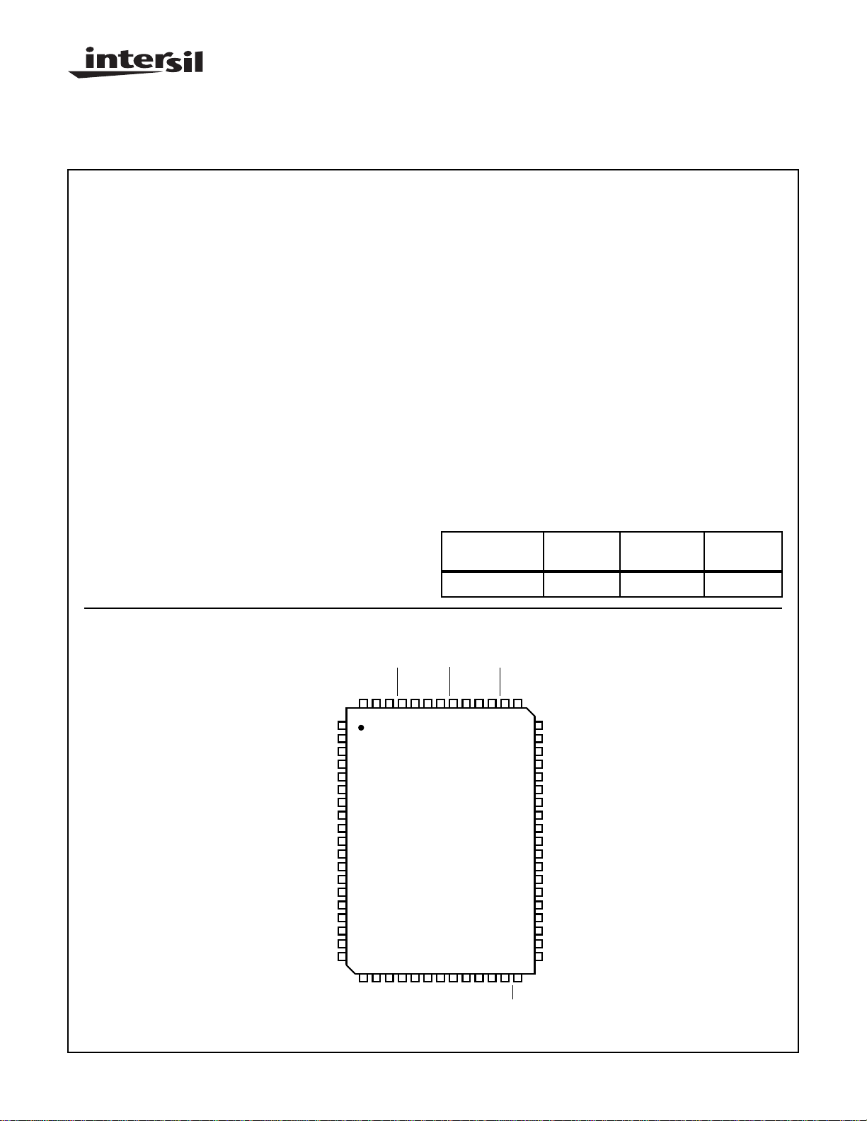
Ordering Information
TEMP.
PART NUMBER
HI3050JCQ -20 to 75 64 Ld MQFP Q64.14x20-S
RANGE (oC) PACKAGE PKG. NO.
Pinout
R0 (LSB)
R1
R2
R3
R4
R5
R6
R7
R8
R9 (MSB)
G0 (LSB)
G1
G2
G3
G4
G5
G6
G7
G8
HI3050 (MQFP)
TOP VIEW
DVDDAVDDAVDDBOUT
6463 62 616059 58 575655 54 5352
1
2
3
4
5
6
7
8
9
10
11
12
13
14
15
16
17
18
19
2021 22 232425 26 272829 30 3132
G9 (MSB)
BOUT
AVDDAVDDGOUT
B1B2B3B4B5B6B8
B0 (LSB)
GOUT
AVDDAVDDROUT
B7
B9 (MSB)
ROUT
51
50
49
48
47
46
45
44
43
42
41
40
39
38
37
36
35
34
33
CE
BLANK
AGND
COMP B
V
OUT B
REF
COMP G
V
OUT G
REF
COMP R
V
OUT R
REF
V
REFB
V
REFG
V
REFR
FS ADJUST B
FS ADJUST G
FS ADJUST R
AGND
V
BIAS
DGND
BCLK
GCLK
RCLK
CAUTION: These devices are sensitive to electrostatic discharge; follow proper IC Handling Procedures.
http://www.intersil.com or 407-727-9207
| Copyright © Intersil Corporation 1999
10-1
File Number 3936.2
Page 2
Functional Block Diagram
R0 (LSB)
G0 (LSB)
B0 (LSB)
R1
R2
R3
R4
R5
R6
R7
R8
R9
G1
G2
G3
G4
G5
G6
G7
G8
G9
B1
B2
B3
B4
B5
B6
B7
B8
B9
1
2
3
4
5
6
7
8
9
10
11
12
13
14
15
16
17
18
19
20
21
22
23
24
25
26
27
28
29
30
DECODER
DECODER
DECODER
DECODER
DECODER
DECODER
LATCHES
LATCHES
LATCHES
HI3050
4 LSBs
CURRENT
CELLS
6 MSBs
CURRENT
CELLS
CLOCK
GENERATOR
CURRENT CELLS
(FOR FULL SCALE)
4 LSBs
CURRENT
CELLS
6 MSBs
CURRENT
CELLS
CLOCK
GENERATOR
CURRENT CELLS
(FOR FULL SCALE)
4 LSBs
CURRENT
CELLS
6 MSBs
CURRENT
CELLS
CLOCK
GENERATOR
CURRENT CELLS
(FOR FULL SCALE)
DV
64
DD
AV
62
DD
AV
63
DD
COMP R
46
ROUT
52
53
ROUT
RCLK
33
45
42
-
+
39
58
59
48
56
57
34
47
43
-
+
40
54
55
50
60
61
35
49
44
-
+
41
OUT R
V
REF
V
REFR
FS ADJUST R
AV
DD
AV
DD
COMP G
GOUT
GOUT
GCLK
OUT G
V
REF
V
REFG
FS ADJUST G
AV
DD
AV
DD
COMP B
BOUT
BOUT
BCLK
OUT B
V
REF
V
REFB
FS ADJUST B
BLANK
CE
BIAS
31
32
VOLTAGE
GENERATOR
V
37
BIAS
AGND
38
AGND
51
DGND
36
10-2
Page 3
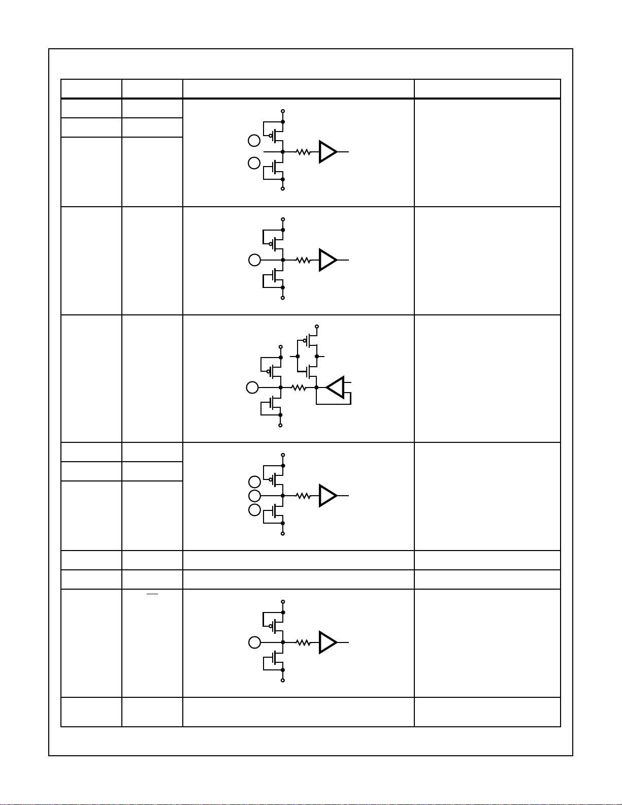
HI3050
Pin Descriptions and Equivalent Circuits
PIN NO. SYMBOL EQUIVALENT CIRCUIT DESCRIPTION
1 - 10 R0 - R9 Digital Inputs.
DV
DD
11 - 20 G0 - G9
21 - 30 B0 - B9
31 BLANK Output Blanking Input.
TO
30
1
DGND
DV
DD
High: Outputs Set to 0mA.
Low: Normal Output Operation.
31
DGND
37 V
BIAS
DV
DD
DV
DD
37
+
-
Internal Bias Decoupling.
Connect a 0.1µF decoupling capacitor
to DGND.
DGND
33 RCLK Clock Inputs.
DV
DD
All input pins are TTL/CMOS compatible.
34 GCLK
35 BCLK
33
34
35
DGND
36 DGND Digital Ground.
38, 51 AGND Analog Ground.
32 CE Chip Enable pin.
DV
DD
High: Part Disabled
Low: Part Enabled
32
DGND
54, 55, 58, 59,
AV
DD
Analog Power Supply.
62, 63
10-3
Page 4
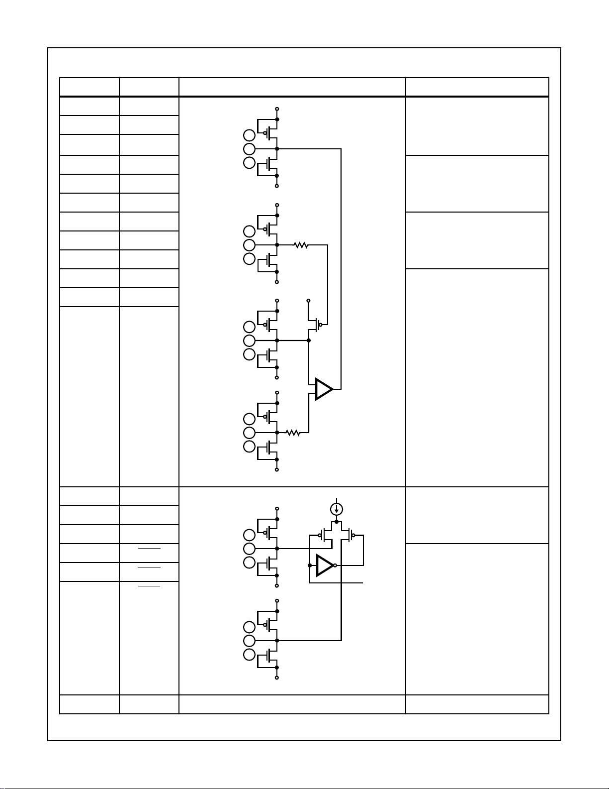
HI3050
Pin Descriptions and Equivalent Circuits
(Continued)
PIN NO. SYMBOL EQUIVALENT CIRCUIT DESCRIPTION
45 V
47 V
49 V
46 COMP R Reference Decoupling.
OUT R Reference Output.
REF
REF
REF
OUT G
OUT B
45
47
49
AV
DD
Typically connected to the Reference
Decoupling inputs (COMP R, COMP G,
COMP B). See Figures 11 and 12 for
various configurations.
Connect a decoupling capacitor (0.1µF)
48 COMP G
50 COMP B
AGND
AV
DD
to reduce noise on reference to AVDD.
39 FS ADJUST R Full Scale Adjust.
40 FS ADJUST G
41 FS ADJUST B
42 V
43 V
44 V
REFR
REFG
REFB
46
48
50
AGND
AV
DD
39
40
41
Typically connect a 1.2kΩ resistor, R
to AGND. R
is used to determine full
SET
scale output current.
Voltage Reference Input.
Typically set to 2V and determines full
scale output current.
I
Full Scale()
OUT
V
REF
---------------
R
SET
,
SET
16×=
AGND
AV
42
43
44
AGND
DD
+
-
52 ROUT Current Outputs.
AV
56 GOUT
60 BOUT
53 ROUT Inverted Current Outputs.
52
56
60
DD
57 GOUT
61 BOUT
53
57
61
AGND
AV
DD
64 DV
DD
AGND
Digital Power Supply.
10-4
Page 5

HI3050
Absolute Maximum Ratings T
Digital Supply Voltage, DVDD to DGND . . . . . . . . . . . . . . . . . . . +7V
Analog Supply Voltage, AVDD to AGND. . . . . . . . . . . . . . . . . . . +7V
Digital Input Voltages . . . . . . . . . . . . . . . . . . . . . . . . DVDD to DGND
Analog Output Current (I
) . . . . . . . . . . . . . . . . . . . . . . . . .30mA
OUT
=25oC Thermal Information
A
Thermal Resistance (Typical, Note 1) θJA (oC/W)
MQFP Package. . . . . . . . . . . . . . . . . . . . . . . . . . . . 80
Maximum Junction Temperature (Plastic Package) . . . . . . . .150oC
Maximum Storage Temperature Range . . . . . . . . . -65oC to 150oC
Maximum Lead Temperature (Soldering 10s). . . . . . . . . . . . . 300oC
(MQFP - Lead Tips Only)
Operating Conditions
Supply Voltage, AVDD, AVSS. . . . . . . . . . . . . . . . . . .4.75V to 5.25V
DVDD, DVSS. . . . . . . . . . . . . . . . . . .4.75V to 5.25V
CAUTION: Stresses above those listed in “Absolute Maximum Ratings” may cause permanent damage to the device. This is a stress only rating and operation
of the device at these or any other conditions above those indicated in the operational sections of this specification is not implied.
NOTE:
1. θJA is measured with the component mounted on an evaluation PC board in free air.
Electrical Specifications AV
= +5V, DVDD = +5V, f
DD
PARAMETER TEST CONDITIONS MIN TYP MAX UNITS
SYSTEM PERFORMANCE
Resolution - 10 - Bits
Maximum Conversion Speed 50 - - MSPS
Integral Linearity Error, INL “Best Fit” Straight Line -2.0 - 2.0 LSB
Differential Linearity Error, DNL -0.5 - 0.5 LSB
Output Offset Voltage, V
Output Full Scale Ratio Error, F
Full Scale Output Current, I
Full Scale Output Voltage, V
OS
FS
FS
SRE
(Note 2) 0 1.5 3 %
Output Voltage Compliance Range - 2.5 - V
DYNAMIC CHARACTERISTICS
Glitch Energy, GE - 50 - pV/s
Settling Time I
= 13.5mA - 40 - ns
OUT
Crosstalk 10MHz Output Sine Wave - 50 - dB
DIGITAL INPUTS
Input Logic High Voltage, V
Input Logic Low Voltage, V
Input Logic Current, I
Input Logic Current, I
Digital Input Capacitance, C
IH
IL
IH
IL
IN
TIMING CHARACTERISTICS
Data Setup Time, t
Data Hold Time, t
SU
HLD
Propagation Delay Time, t
Clock Pulse Width, t
PW1
, t
PD
PW0
See Figure 1 - 5 7 ns
See Figure 1 - 1 3 ns
See Figure 1 - 10 - ns
See Figure 1 10 - - ns
POWER SUPPLY CHARACTERISITICS
Total Supply Current, AI
Analog Supply Current, AI
Digital Supply Current, DI
DD
DD
DD
+ DI
DD
Power Dissipation - 500 550 mW
NOTE:
2. Configured for Common Reference.
F
SRE
Full Scale Voltage of Channel
------------------------------------------------------------------------------------------------------------------ 1– 100%×=
Average Full Scale Voltage of All Channels
Clock Pulse Width (t
Temperature Range (T
= 50MHz, RL = 75Ω, V
CLK
, t
PW1
OPR
REF
) . . . . . . . . . . . . . . . . . . . .10ns (Min)
PW0
) . . . . . . . . . . . . . . . . . . . .-20oC to 75oC
= 2V, R
= 1.2kΩ, TA = 25oC
SET
--1mV
-2730mA
1.8 1.9 2.0 V
2.0 - - V
- - 0.8 V
--5µA
-5 - - µA
-10-pF
- 100 110 mA
-92-mA
-8-mA
10-5
Page 6

Timing Diagram
t
PW1
t
PW0
HI3050
CLK
t
SU
R9-R0
G9-G0
B9-B0
ROUT
GOUT
BOUT
t
PD
FIGURE 1. PROPAGATION DELAY, SETUP TIME, HOLD TIME AND MINIMUM PULSE WIDTH DIAGRAM
Typical Performance Curves
80
70
t
HLD
50%
t
SU
t
HLD
t
PD
110
t
SU
t
HLD
100%
50%
t
PD
0%
60
CROSSTALK (dB)
50
VDD = 5.0V, TA = 25oC
40
100K 1M 10M
OUTPUT FREQUENCY (Hz)
FIGURE 2. CROSSTALK vs OUTPUT FREQUENCY
1.9
FULL-SCALE VOLTAGE (V)
1.8
VDD = 5.0V, V
-20 0 70
= 2.0V
REF
25 50
AMBIENT TEMPERATURE (oC)
VDD = 5.0V, f
= 2.0V
V
SUPPLY CURRENT (mA)
100
REF
-20 0 75
AMBIENT TEMPERATURE (oC)
FIGURE 3. SUPPLY CURRENT vs AMBIENT TEMPERATURE
70
65
60
55
50
SFDR (dB)
45
40
35
30
0.1 1.0 10.0
OUTPUT FREQUENCY (MHz)
CLK
= 50MHz
25 50
FIGURE 4. FULL SCALE VOLT AGE vs AMBIENT TEMPERATURE FIGURE 5. SFDR vs OUTPUT FREQUENCY
10-6
Page 7

HI3050
DAC INPUT/OUTPUT CODE TABLE (NOTE 1)
INPUT CODE
MSB
D9 D8 D7 D6 D5 D4 D3 D2 D1
1111111111 2.0V
•
•
•
1000000000 1.0V
•
•
•
0000000000 0V
NOTE:
1. V
REF
= 2.0V, R
SET
= 1.2K, R
LOAD
= 75Ω.
LSB
D0
OUTPUT VOLTAGE
Detailed Description
The HI3050 contains three matched, individual, 10 bit current
output digital-to-analog converters. The DACs can convert at
50MHz and run on +5V for both the analog and digital supplies.
The architecture is a current cell arrangement. 10-bit linearity is
obtained without laser trimming due to an internal calibration.
Digital Inputs
The digital inputs to the HI3050 have TTL level thresholds.
Due to the low input currents CMOS logic can be used as
well. The digital inputs are latched on the rising edge of the
clock.
To reduce switching noise from the digital data inputs, a
series termination resistor is the best solution. Using a 50Ω
to 130Ω resistor in series with the data lines, the edge rates
are slowed. Slower edge rates reduce the amount of overshoot and undershoot that directly couples through the lead
frame of the device. TTL drivers such as the 74ALS or 74F
series or CMOS logic series drivers, ACT, AC, or FCT, are
excellent for driving the TTL/CMOS inputs of the converter.
Clocks and Termination
The HI3050 clock rate can run to 50MHz, therefore, to minimize
reflections and clock noise into the part, proper termination
should be considered. In PCB layout clock tr aces should be k ept
short and have a minimum of loads. To guarantee consistent
results from board to board controlled impedance traces should
be used with a characteristic line impedance.
To terminate the clock line, a shunt terminator to an AC ground
is the most effective type at a 50MHz clock rate. Shunt termination is best used at the receiving end of the transmission line
or as close to the HI3050 CLK pin as possible.
HI3050
= 50Ω
Z
O
RT = 50Ω
FIGURE 6. AC TERMINATION OF THE HI3050 CLOCK LINE
CLK
DAC
Rise and fall times and propagation delay of the line will be
affected by the Shunt Terminator. The terminator can be
connected to DGND.
Power Supplies
To reduce power supply noise, separate analog and digital
power supplies should be used with 0.1µF and 0.01µF cer amic
capacitors placed as close to the body of the HI3050 as
possible on the analog (A V
) and digital (DVDD) supplies. The
DD
analog and digital ground returns should be connected together
at the device to ensure proper operation on power up.
Reference
The HI3050 DACs have their own references and can be set
individually, see Figure 13. The three references can also
share a common reference voltage, see Figure 12. A shared
reference gives DAC to DAC matching of 1.5%, typically.
The HI3050 requires an external reference voltage to set the
full scale output current. The external reference voltage is
connected to the V
inputs (V
REF
REFR
, V
REFG
, and
VREFB). The Full Scale Adjust input (FS ADJUST R, FS
ADJUST G, FS ADJUST B) should be connected to AGND
through a 1.2kΩ resistor, R
(V
OUT R, V
REF
REF
OUT G, V
. The reference outputs
SET
OUT B) should be con-
REF
nected to the decoupling input (COMP R, COMP G,
COMP B) and decoupled to AV
with a 0.1µF capacitor.
DD
This improves settling time by decoupling switching noise
from the reference output of the HI3050.
The full scale output current is controlled by the voltage
reference pin and the set resistor (R
I
(Full Scale) = (V
OUT
REF/RSET
) x 16, I
). The ratio is:
SET
is in mA (EQ.1)
OUT
Blanking Input
The BLANK input, when pulled high, will force the outputs of
all three DACs to 0mA.
Chip Enable
The chip enable input,
CE, will shut down the HI3050
causing the outputs to go to 0mA. The analog and digital
supply current will decrease to less than 1mA, reducing
power for low power applications.
10-7
Page 8

HI3050
Outputs
The HI3050 DAC outputs are complementary current outputs. Current is steered to either I
OUT
or I
in proportion
OUT
to the digital input code. The current output can be converted
to a voltage by using a resistor load or I/V converting op
amp. If only one output of a converter is being used, the
unused output can be connected to ground or to a load
equal to the used output. The output voltage when using a
resistor load is:
V
= I
OUT
OUT
x R
OUT
(EQ. 2)
The compliance range of the outputs is from 0V to +2.5V.
To convert the output current of the D/A converter to a volt-
age a load resistor followed by a buffer amplifier can be used
as shown in Figure 5. The DAC needs a 75Ω termination
resistor on the I
HI3050
DAC
I
OUT
FIGURE 7. HIGH SPEED CURRENT TO VOLTAGE CONVERSION
pin to ensure proper settling.
OUT
-
+
75Ω
1/3 HA5013
75Ω
75Ω
to change before another. To minimize this, the Intersil
HI3050 employs an internal register, just prior to the current
sources, that is updated on the clock edge.
In measuring the output glitch of the HI3050, the output is
terminated into a 75Ω load. The glitch is measured at the
major carries throughout the DACs output range.
HI3050
I
OUT
75Ω
FIGURE 8. GLITCH TEST CIRCUIT
50MHz
LOW PASS
FILTER
SCOPE
50Ω
The glitch energy is calculated by measuring the area under
the voltage-time curve. Figure 9 shows the area considered
as glitch when changing the DAC output. Units are typically
specified in picoVolt/seconds (pV/s).
V
HEIGHT (H)
Glitch
The output glitch of the HI3050 is measured by summing the
area under the switching transients after an update of the
DAC. Glitch is caused by the time skew between bits of the
incoming digital data. Typically the switching time of digital
inputs are asymmetrical meaning that the turn off time is
faster than the turn on time (TTL designs). Unequal delay
paths through the device can also cause one current source
Test Circuits
R0 - R9
31
32
37
33
34
35
1 - 10
G0 - G9
11 - 20
B0 - B9
21 - 30
BLK
CE
VB
RCLK
GCLK
BCLK
CLK
50MHz
SQUARE WAVE
10-BIT
COUNTER
WITH LATCH
0.1µF
DGND
R0
R0
G0
G0
B0
B0
46, 48, 50
45, 47, 49
42 - 44
39 - 41
WIDTH (W)
GLITCH AREA =
1
/2 (H X W)
T (ps)
FIGURE 9. GLITCH ENERGY
52
53
56
57
60
61
AV
DD
2V
1.2kΩ
0.1
µF
75Ω
AGND
OSCILLOSCOPE
75Ω
AGND
75Ω
AGND
FIGURE 10. MAXIMUM CONVERSION SPEED TEST CIRCUIT
10-8
Page 9

HI3050
Test Circuits
CLK
50MHz
SQUARE WAVE
(Continued)
10-BIT
COUNTER
WITH LATCH
DELAY
CONTROLLER
DELAY
CONTROLLER
FIGURE 11. SETUP HOLD TIME AND GLITCH ENERGY TEST CIRCUIT
DGND
0.1µF
31
32
37
33
34
35
R0 - R9
1 - 10
G0 - G9
11 - 20
B0 - B9
21 - 30
BLK
CE
VB
RCLK
GCLK
BCLK
R0
R0
G0
G0
B0
B0
46, 48, 50
45, 47, 49
42 - 44
39 - 41
52
53
56
57
60
61
AV
DD
2V
1.2kΩ
0.1
µF
75Ω
AGND
OSCILLOSCOPE
75Ω
AGND
75Ω
AGND
CLK
SQUARE WAVE
50MHz
DIGITAL
WAVEFORM
GENERATOR
ALL “1”
0.1µF
DGND
31
32
37
33
34
35
R0 - R9
1 - 10
G0 - G9
11 - 20
B0 - B9
21 - 30
BLK
CE
VB
RCLK
GCLK
BCLK
R0
R0
G0
G0
B0
B0
46, 48, 50
45, 47, 49
42 - 44
39 - 41
52
53
56
57
60
61
FIGURE 12. CROSSTALK TEST CIRCUIT
AV
DD
0.1
µF
2V
1.2kΩ
75Ω
AGND
OSCILLOSCOPE
75Ω
AGND
75Ω
AGND
10-9
Page 10

Applications Circuits
HI3050
1kΩ
GOUT
75Ω
ROUT
BOUT
75Ω
75Ω
0.1µF
1.2kΩ
NC
NC
4847 46 454443 42 414039 38 373635 34 33
5150 49
52
53
54
55
56
57
58
59
60
61
62
63
64
12345678910111213141516
NC NC
0.1
µF
1718 19
G CHANNEL INPUTR CHANNEL INPUT
FIGURE 13. COMMON VOLTAGE REFERENCE
1kΩ
CLOCK INPUT
32
31
30
29
28
27
26
25
24
23
22
21
20
B CHANNEL INPUT
AV
DD
AGND DGND
DV
DD
GOUT
75Ω
ROUT
BOUT
75Ω
75Ω
1kΩ
1kΩ
0.1µF
52
53
54
55
56
57
58
59
60
61
62
63
64
0.1µF0.1
µF
1.2kΩ
1.2kΩ
1.2kΩ
4847 46 454443 42 414039 38 373635 34 33
5150 49
12345678910111213141516
G CHANNEL INPUTR CHANNEL INPUT
0.1
µF
1718 19
CLOCK INPUT
32
31
30
29
28
27
26
25
24
23
22
21
20
B CHANNEL INPUT
AV
DD
AGND DGND
DV
DD
FIGURE 14. INDEPENDENT REFERENCES
10-10
Page 11

Definition of Specifications
HI3050
Integral Linearity Error, INL, is the measure of the worst
case point that deviates from a best fit straight line of data
values along the transfer curve.
Differential Linearity Error, DNL, is the measure of the
step size output deviation from code to code. Ideally the step
size should be 1 LSB. A DNL specification of 1 LSB or less
guarantees monotonicity.
Crosstalk, is the undesirable signal coupling from one
channel to another.
Feedthrough, is the measure of the undesirable switching
noise coupled to the output.
Output Voltage Full Scale Settling Time, is the time
required from the 50% point on the clock input for a full scale
step to settle within an
1
/2 LSB error band.
Output Voltage Small Scale Settling Time, is the time
required from the 50% point on the clock input for a 100mV
step to settle within an
1
/2 LSB error band. This is used by
applications reconstructing highly correlated signals such as
sine waves with more than 5 points per cycle.
Glitch Energy, GE, is the switching transient appearing on
the output during a code transition. It is measured as the
area under the curve and expressed as a Volt-Time
specification.
Differential Gain, DG, is the peak difference in chrominance
amplitude (in percent) at two different DC levels.
Differential Phase, DP, is the peak difference in
chrominance phase (in degrees) at two different DC levels.
Signal to Noise Ratio, SNR, is the ratio of a fundamental to
the noise floor of the analog output. The first 5 harmonics
are ignored, and an output filter of
1
/2 the clock frequency is
used to eliminate alias products.
Total Harmonic Distortion, THD, is the ratio of the DAC
output fundamental to the RMS sum of the harmonics. The
first 5 harmonics are included, and an output filter of
1
/2 the
clock frequency is used to eliminate alias products.
Spurious Free Dynamic Range, SFDR, is the amplitude
difference from a fundamental to the largest harmonically or
non-harmonically related spur. A sine wav e is loaded into the
D/A and the output filtered at
1
/2 the clock frequency to
eliminate noise from clocking alias terms.
Intermodulation Distortion, IMD, is the measure of the
sum and difference products produced when a two tone
input is driven into the D/A. The distortion products created
will arise at sum and difference frequencies of the two tones.
IMD is:
20 Log (RMS of Sum and Difference Distortion Products)
IMD
-------------------------------------------------------------------------------------------------------------------------------------------------------=
RMS Amplitude of the Fundamental()
All Intersil semiconductor products are manufactured, assembled and tested under ISO9000 quality systems certification.
Intersil products are sold by description only. Intersil Corporation reser ves the right to make changes in circuit design and/or specifications at any time without
notice. Accordingly, the reader is cautioned to verify that data sheets are current before placing orders. Information furnished by Intersil is believed to be accurate
and reliable. However, no responsibility is assumed by Intersil or its subsidiaries for its use; nor for any infringements of patents or other rights of third parties which
may result from its use. No license is granted by implication or otherwise under an y patent or patent rights of Intersil or its subsidiaries.
For information regarding Intersil Corporation and its products, see web site http://www.intersil.com
10-11
 Loading...