

Page 1
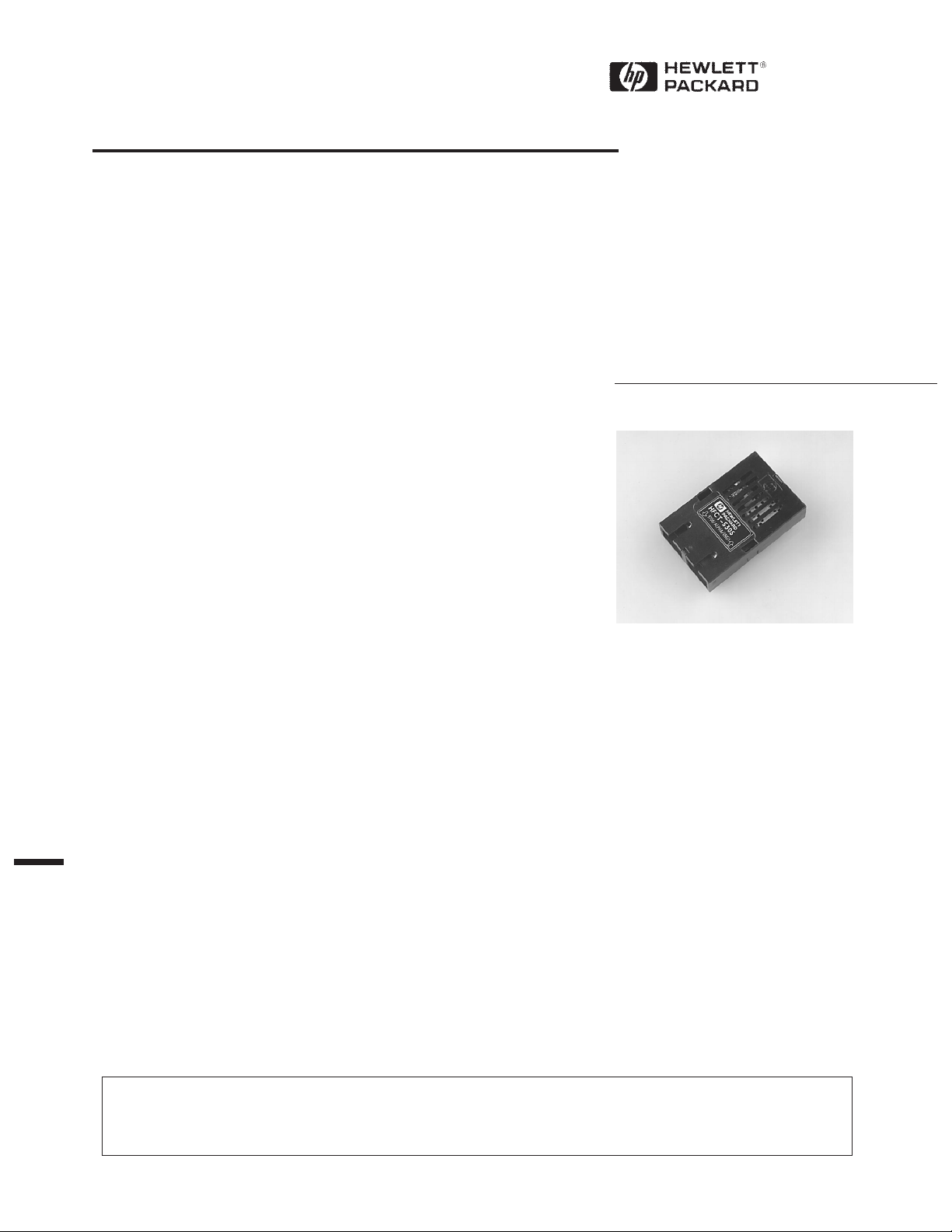
Gigabit Ethernet: 1.25 GBd
1300 nm Laser Transceiver
in Low Cost 1 x 9 Package Style
Preliminary Technical Data
HFCT-5305
Features
• Compliant with Proposed
Specifications for IEEE802-3 Gigabit Ethernet
• 1300 nm Trenched BH Laser
Source Technology
• Industry Standard 1 x 9
Package Style with Integral
Duplex SC Connector
• Class 1 Laser Safety
(Certification Pending)
• 3 km Links in 8/125 µm SMF
Cables
• 550 m Links in 62.5/125 µm
MMF Cables
• Single +5 V Power Supply
Operation and PECL Logic
Interfaces
• Wave Solder and Aqueous
Wash Process Compatible
• Designed and Manufactured
in an ISO 9000 Certified
Facility
Applications
• Host to Host Interface
Description
General Transmitter Section
The transmitter section consists
of a 1300 nm Laser in an eye safe
optical subassembly, (ELSA),
which mates to the fiber cable.
The ELSA is driven by a custom
silicon bipolar IC which converts
differential PECL logic signals,
ECL referenced to a +5 V supply,
into an analog Laser Diode drive
current.
Eye Safety Design
The ELSA is designed to be eye
safe under a single fault condition. To be eye-safe, only one of
two results can occur in the event
of a single fault. The transmitter
must either maintain a safe level
of output power or the transmitter should be disabled.
The ELSA contains a patented
optical fiber stub which restricts
the level of light emerging from
the connector port under all
conditions. Overdriving the laser
(even to destruction) cannot
produce enough light to violate
the IEC safe level. As a result the
HFCT-5305 is intrinsically eye
safe.
Receiver Section
The receiver includes an InP PIN
photodiode mounted together
with a custom silicon bipolar
transimpedance preamplifier IC
in an optical subassembly, OSA.
This OSA is mated to a custom
silicon bipolar circuit providing
post-amplification and
quantization.
The custom silicon bipolar circuit
also includes a Signal Detect
circuit which provides a PECL
logic high output upon detection
of a usable input optical signal
level. This single-ended lowpower PECL output is designed
to drive a standard PECL input
Preliminary Product Disclaimer
This preliminary data sheet is provided to assist you in the evaluation of engineering samples of the product which is under development
and targeted for release during 1997. Until Hewlett-Packard releases this product for general sales, HP reserves the right to alter prices,
specifications, features, capabilities, function, manufacturing release dates, and even general availability of the product at any time.
(5/97)
565
Page 2

through a 10 Ω load instead of
the normal 50 Ω ECL load.
Regulatory Compliance
See the Regulatory Compliance
Table for the targeted typical
and measured performance for
these transceivers. As the
product design is completed,
full characterization testing
will be done to determine the
actual performance of the final
design.
The overall equipment design will
determine the level it is able to be
certified to. These transceiver
performance targets are offered
as a figure of merit to assist the
designer in considering their use
in equipment designs.
Electrostatic Discharge (ESD)
There are two design cases in
which immunity to ESD damage
is important.
The first case is during handling
of the transceiver prior to mounting it on the circuit board. It is
important to use normal ESD
handling precautions for ESD
sensitive devices. These precautions include using grounded
wrist straps, work benches, and
floor mats in ESD controlled
areas.
The targeted performance has
been shown to provide adequate
performance typical industry
production environments.
The second case to consider is
static discharges to the exterior
of the equipment chassis
containing the transceiver parts.
To the extent that the duplex SC
connector is exposed to the
outside of the equipment chassis
it may be subject to whatever
system level ESD test criteria that
the equipment is intended to
meet. The targeted performance
is more robust than typical
industry equipment practices
today.
Electromagnetic Interference
(EMI)
Most equipment designs utilizing
these high speed transceivers
from Hewlett-Packard will be
required to meet the requirements of FCC in the United
States, CENELEC EN55022
(CISPR 22) in Europe and VCCI
in Japan.
These transceivers, with their
shielded design, are targeted to
perform to the limits listed to
assist the designer in the
management of the overall
equipment EMI performance.
Immunity
Equipment utilizing these
transceivers will be subject to
radio-frequency electromagnetic
fields in some environments.
Regulatory Compliance
Feature Test Method Targeted Performance
Electrostatic Discharge MIL-STD-883C Class 1 (>500 V)
(ESD) to the Method 3015.4
Electrical Pins
Electrostatic Discharge Variation of IEC 801-2 Products of this type will typically withstand at
(ESD) to the least 25 kV without damage when the Duplex
Duplex SC Receptacle SC Connector Receptacle is contacted by a
Human Body Model probe.
Electromagnetic FCC Class A Typically provide a TBD dB margin to the noted
Interference (EMI) CENELEC EN55022 Class A standard limits when tested at a certified test
(CISPR 22A) range with the transceiver mounted to a circuit
VCCI Class I card without a chassis enclosure.
Immunity Variation of IEC 801-3 Typically show no measurable effect from a
3 V/m field swept from 10 to 450 MHz applied
to the transceiver without a chassis enclosure.
Eye Safety FDA CDRH 21-CFR 1040 Class Compliant per Hewlett-Packard Testing for all
1 IEC 825 Issue 1 1993: three requirements under normal operating
11 Class conditions. Fault condition testing pending
1 CENELEC EN60825 Class 1 completion of product development.
566
Page 3
These transceivers have an
immunity to such fields due to
their shielded design.
provide Class 1 eye safety by
design. Hewlett-Packard has
tested the current transceiver
design is completed. HP will
obtain certification from outside
sources for eye safety.
design for compliance with the
Eye Safety
These 1300 nm Laser-based
transceivers are intended to
requirements listed below under
normal operating conditions and
will test for compliance under
fault conditions when the product
This performance will enable the
transceivers to be used without
concern for eye safety in the
same way that LED-based
transceivers are used today.
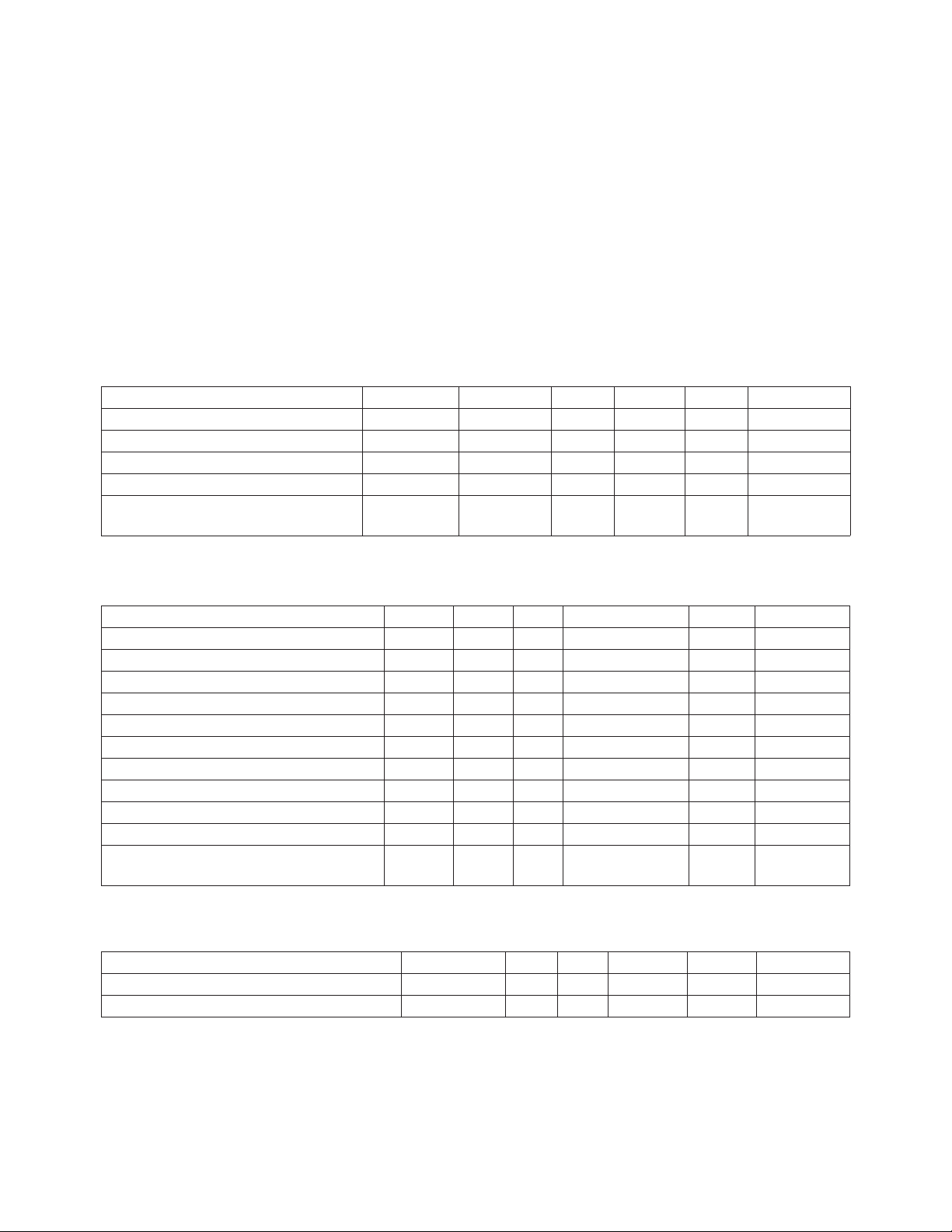
Absolute Maximum Ratings
Parameter Symbol Min. Typ. Max. Unit Reference
Storage Temperature T
Ambient Operating Temperature T
Supply Voltage V
Data Input Voltage V
Transmitter Differential Input V
S
A
CC
I
D
–40 +100 °C
–10 +80 °C
–0.5 7 V
–0.5 V
CC
V
See Table 1.4 V 1
Voltage Below
Recommended Operating Conditions
Parameter Symbol Min. Typ. Max. Unit Reference
Ambient Operating Temperature T
A
Relative Humidity RH 5 95 %
Supply Voltage V
CC
Power Supply Ripple TBD Hz/V
Power Supply Rejection TBD Hz/V
Transmitter Data Input Voltage - Low VIL-V
CC
Transmitter Data Input Voltage - High VIH-VCC–1.165 –0.880 V 2
Transmitter Differential Input Voltage V
Data Output Load R
Signal Detect Output Load R
D
DL
SDL
Conducted Noise on Data and Signal TBD Hz/V
Detect Outputs
0 +70 °C
4.75 5.25 V
pp
pp
–1.810 –1.475 V 2
0.3 See Table Above V
50 Ω 3
710 Ω 4
pp
Process Compatibility
Parameter Symbol Min. Typ. Max. Unit Reference
Hand Lead Soldering Temperature/Time T
Wave Soldering and Aqueous Wash T
Notes:
1. This is the maximum voltage that can be applied across the Differential Transmitter Data Inputs without damaging the ESD
protection circuit.
2. Compatible with 10 K, 10 KH and 100 K ECL and PECL signals.
3. The outputs are terminated to VCC - 2 V.
4. The outputs are terminated to ground.
SOLD/tSOLD
SOLD/tSOLD
+270/10 °C/sec.
+270/10 °C/sec.
567
Page 4

Transmitter Electrical Characteristics
(TA = 0°C to +70°C, VCC = 4.75 V to 5.25 V)
Parameter Symbol Min. Typ. Max. Unit Reference
Supply Current I
Power Dissipation P
Data Input Current – Low I
Data Input Current – High I
CCT
DIST
IL
IH
Receiver Electrical Characteristics
(TA = 0°C to +70°C, VCC = 4.75 V to 5.25 V)
Parameter Symbol Min. Typ. Max. Unit Reference
Supply Current I
Power Dissipation P
Data Output Voltage – Low V
Data Output Voltage – High V
Data Output Rise Time t
Data Output Fall Time t
Signal Detect Output Voltage – Low V
Signal Detect Output Voltage – High V
Signal Detect Assert Time t
(Off to On)
Signal Detect Assert Time t
(On to Off)
OL
OH
OL
OH
CCR
DISR
– V
– V
r
f
– V
– V
SDA
SDD
65 130 mA 5
0.35 0.68 W
–350 0 µA
16 350 µA
100 120 mA
0.4 0.5 W 6
–1.950 –1.620 V 7
CC
–1.045 –0.740 V 7
CC
0.2 0.3 0.51 ns 8
0.2 0.3 0.51 ns 8
–1.840 –1.620 V 7
CC
–1.045 –0.880 V 7
CC
TBD µs9
TBD µs10
Notes:
5. The typical value is at +70°C; maximum value is an end of life value.
6. Power dissipation value is the power dissipated in the receiver itself. It is calculated as the sum of the products of VCC and I
minus the sum of the products of the output voltages and currents.
7. These outputs are compatible with 10 K, 10 KH and 100 K ECL and PECL inputs.
8. These values are under review and may be replaced by an eye mask test.
9. The Signal Detect output will change from logic “0” to “1” within TBD us of a step transition in optical input power from no light
to –18 dBm.
10. The Signal Detect output will change from logic “1” to “0” within TBD us of a step transition in optical input power from –16 dBm
to no light.
CC
568
Page 5

Transmitter Optical Characteristics
(TA = 0°C to +70°C, VCC = 4.75 V to 5.25 V)
Parameter Symbol Min. Typ. Max. Unit Reference
Output Optical Power P
O
–13 –3 dBm avg.
62.5/125 µm, NA = 0.275 fiber
Optical Extinction Ratio 9 dB
Center Wavelength λC 1270 1355 nm
Spectral Width – rms σ 4 nm rms
RIN
12
–116 dB/Hz
Receiver Optical Characteristics
(TA = 0°C to +70°C, VCC = 4.75 V to 5.25 V)
Parameter Symbol Min. Typ. Max. Unit Reference
Input Optical Power P
IN
Minimum
Return Loss 12 dB
Signal Detect – Asserted P
Signal Detect – Deasserted P
Signal Detect – Hysteresis PA – P
Note:
11. The sensitivity is provided at a BER of 1 x 10
A
D
D
-12
.
–3 –20 dBm avg. 11
PD + 1.5 dB dBm avg.
–45 dBm avg.
1.5 dB
569
Page 6
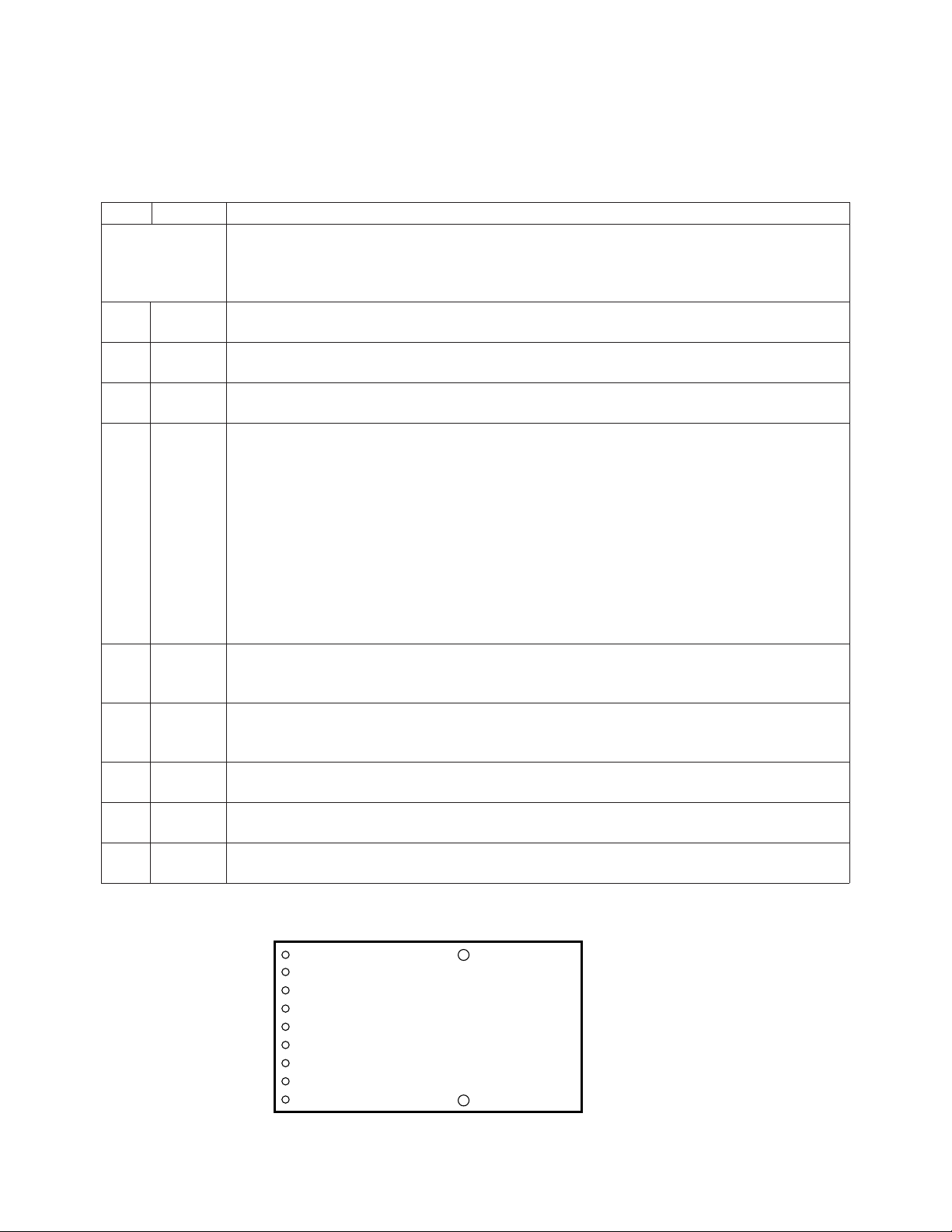
Table 1. Pinout Table
Pin Symbol Functional Description
Mounting Studs The mounting studs are provided for transceiver mechanical attachment to the circuit
board, they are embedded in the nonconductive plastic housing and are not tied to the
transceiver internal circuit. They should be soldered into plated-through holes on the
printed circuit board.
1V
EER
2 RD+ Receiver Data Out
3 RD– Receiver Data Out Bar
4 SD Signal Detect
5V
6V
CCR
CCT
7 TD– Transmitter Data In Bar
8 TD+ Transmitter Data In
9V
EET
Receiver Signal Ground
Directly connect this pin to receiver signal ground plane.
See recommended circuit schematic.
See recommended circuit schematic.
Normal optical input levels to the receiver result in a logic “1” output.
Low optical input levels to the receiver result in a fault condition indication shown by
a logic “0” output.
Signal Detect is a single-ended, low-power, PECL output. Since SD is a low-power
PECL output, complete the interconnection of SD output with other PECL inputs using
a 10 kΩ pull-down resistor to VEE to allow biasing of this interconnection. Do not load
this SD output with standard PECL, 50 Ω to V
– 2 V, termination. If Signal Detect
CC
output is not used, leave it open-circuited.
This Signal Detect output can be used to drive a PECL input on an upstream circuit,
such as, Signal Detect input or Loss of Signal-bar.
Receiver Power Supply
Provide +5 V dc via the recommended transmitter power supply filter circuit.
Locate the power supply filter circuit as close as possible to the V
CCR
pin.
Transmitter Power Supply
Provide +5 V dc via the recommended transmitter power supply filter circuit.
Locate the power supply filter circuit as close as possible to the V
CCT
pin.
See recommended circuit schematic.
See recommended circuit schematic.
Transmitter Signal Ground
Directly connect this pin to the transmitter signal ground plane.
RECEIVER SIGNAL GROUND
RECEIVER DATA OUT
RECEIVER DATA OUT BAR
SIGNAL DETECT
RECEIVER POWER SUPPLY
TRANSMITTER POWER SUPPLY
TRANSMITTER DATA IN BAR
TRANSMITTER DATA IN
TRANSMITTER SIGNAL GROUND
Figure 1. Pinout.
570
1
2
3
4
5
6
7
8
9
TOP VIEW
N/C
N/C
Page 7
A
C
B
AREA
RESERVED
FOR
PROCESS
PLUG
K (8 x 2.54 mm)
H
D
E
J
H
DIM.
MIN. TYP. MAX. MIN. TYP. MAX.
A
B
C
0.25
D
2.92
E
F*
G
H
J
K
*PRE-RELEASE SAMPLES MAY HAVE HEIGHT UP TO
10.35 mm (0.407 INCHES).
F
G
MILLIMETERS INCHES
39.6
12.7
25.4
0.38
3.68
9.8
20.32
15.9
20.32
20.32
0.500
0.010
0.115
0.800
0.626
0.800
0.800
1.559
1.000
0.015
0.145
0.386
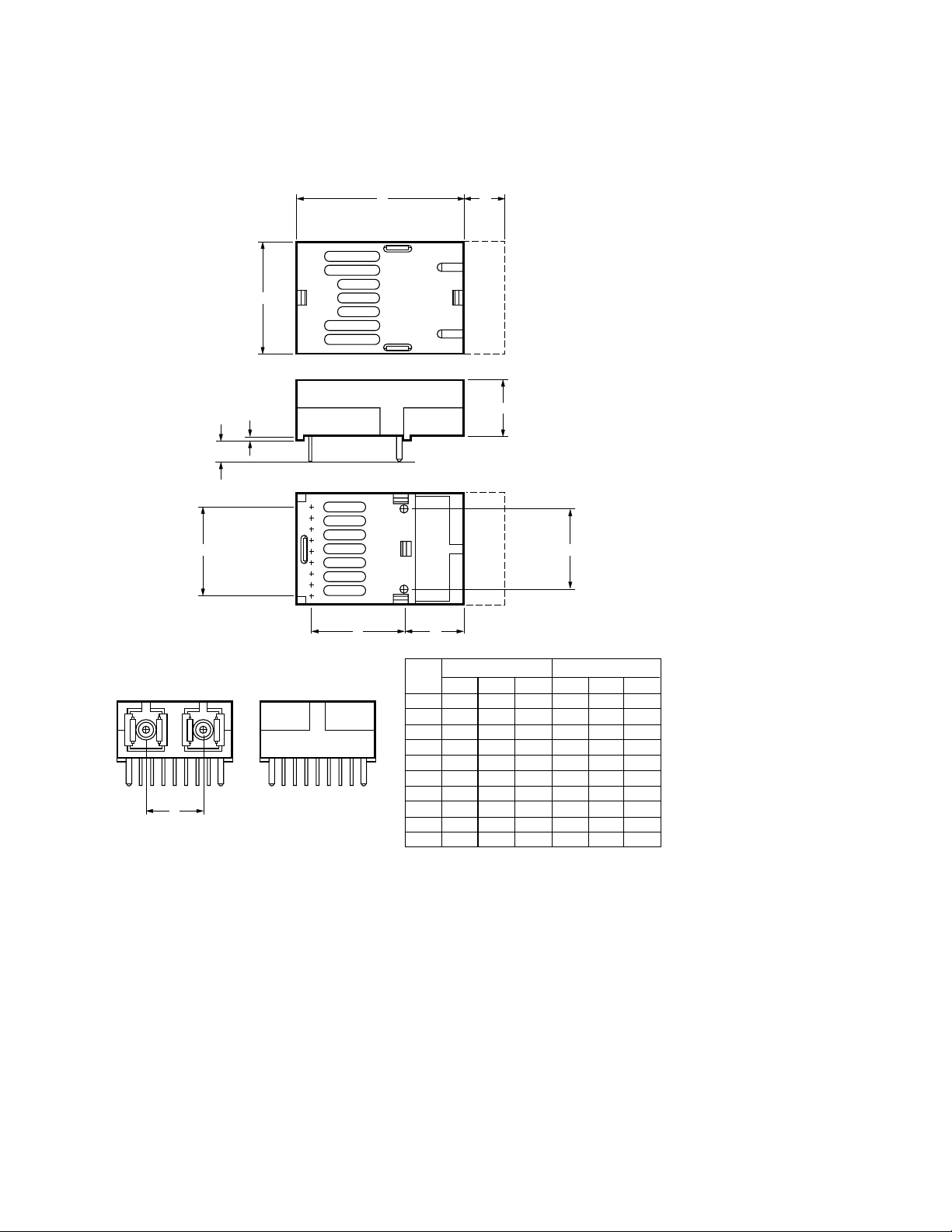
Figure 2. Package Outline Drawing and Pinout.
571
Page 8
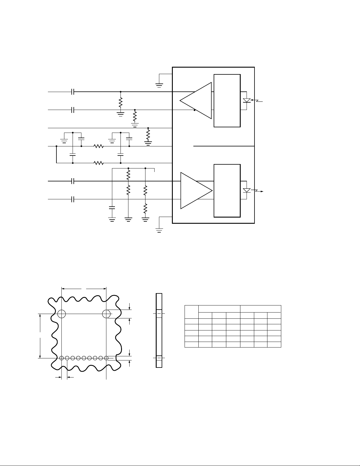
1
RD
RD-
SD
V
CC
TD-
TD
C1 = C2 = C3 = C4 = C5 = 0.01 µF
C6 = C7 = C8 = C9 = 0.01 µF
R1 = R3 = 68 Ω
R2 = R4 = 192 Ω
R5 = R6 = 270 Ω
R7 = 10 kΩ
L1 = L2 = 1 µH
C4
C5
C6
C7
C1
C2
2
R5
R6
R4
R7
V
CC
C8
L1
L2
C3
C9
R1
R2 R3
ELECTRICAL
3
PECL OUTPUT STAGE
4
5
6
7
8
PECL INPUT STAGE
9
SERIAL
OUTPUT
ELECTRICAL
SERIAL
INPUT
RECEIVER
CIRCUITRY
1 x 9 LASER
SERIAL MODULE
LASER
DRIVER
CIRCUITRY
Figure 3. Recommended Circuit Schematic.
A
∅D
B
∅E
C
TOP VIEW
Figure 4. Recommended Board Layout Hole Pattern.
DIM.
∅D
∅E
MILLIMETERS INCHES
MIN. TYP. MAX. MIN. TYP. MAX.
–
1.8
0.7
20.32
–
20.32
–
A
B
C
2.54
–
–
2.0
0.9
–
–
–
0.071
0.028
–
0.800
0.800
0.100
–
–
–
–
–
0.079
0.036
–
–
572
 Loading...