

Page 1
125 Megabaud Fiber Optic
Transceiver
JIS FO7 Connection
Technical Data
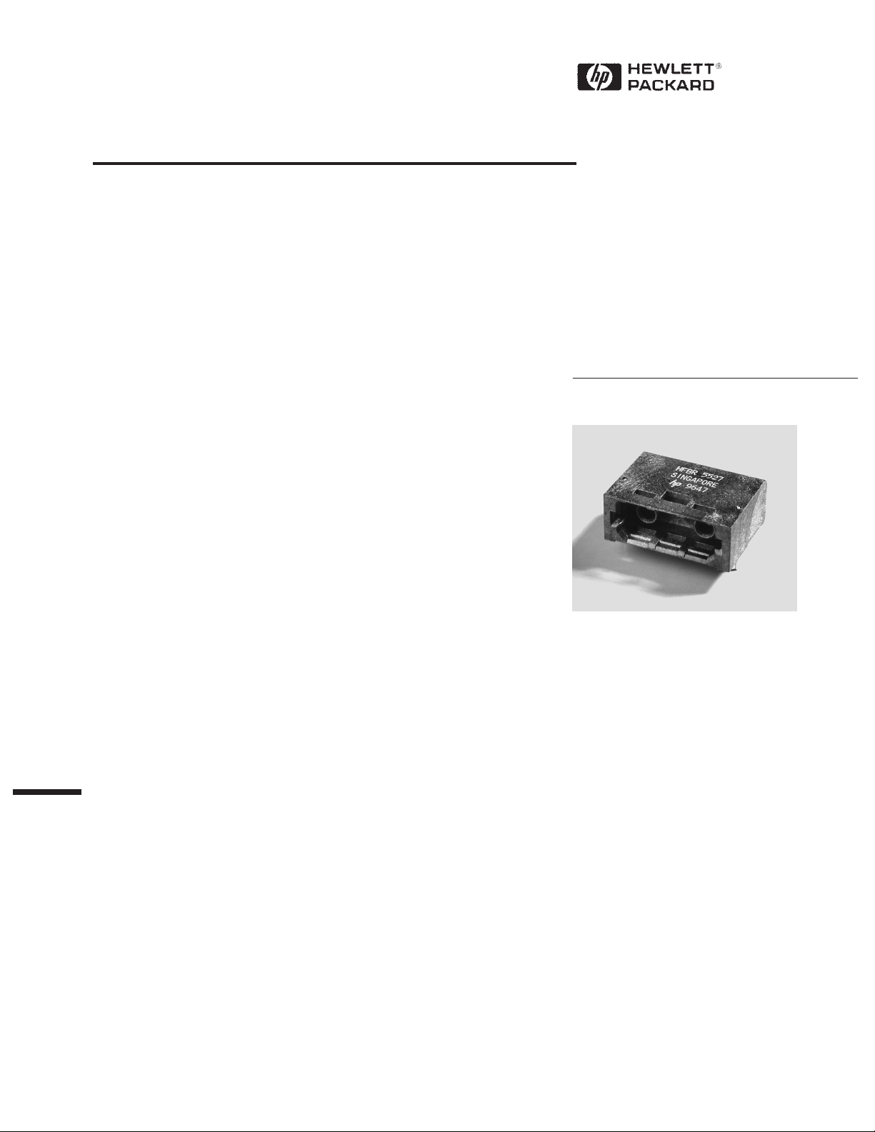
HFBR-5527
Features
• Data Transmission at Signal
Rates of 1 to 125 MBd over
Distances up to 100 Meters
• Compatible with Duplex JIS
FO7 and Simplex JIS FO5
Connectors
• Specified for Use with
Plastic Optical Fiber (POF),
and with Large Core Silica
Fiber (HCS®)
• Transmitter and Receiver
Application Circuit
Schematics Available
• Conductive Plastic Housing
Provides Electrical Shield
Applications
• Intra-System Links: Boardto-Board, Rack-to-Rack
• High Voltage Isolation
• Telecommunications
Switching Systems
• Computer-to-Peripheral Data
Links, PC Bus Extension
• Industrial Control Networks
• Proprietary LANs
• Digitized Video
• Medical Instruments
• Immune to Lightning and
Voltage Transients
Description
The 125 MBd transceiver is a
cost-effective fiber-optic solution
for transmission of 125 MBd data
up to 100 meters with HCS
fiber. The data link consists of a
650 nm visible, red LED transmitter and a PIN/preamp receiver.
These can be used with low-cost
plastic or hard clad silica fiber.
One millimeter diameter plastic
fiber provides the lowest cost
solution for distances under 25
meters. The lower attenuation of
HCS® fiber allows data transmission over longer distance. These
components can be used for high
speed data links without the
problems common with copper
wire solutions.
The transmitter is a high power
650 nm LED. Both transmitter
and receiver are molded in one
housing which is compatible with
the FO7 connector. This connector is designed to efficiently
couple the power into POF or
HCS® fiber.
®
With the recommended drive
circuit, the LED operates at
speeds from 1-125 MBd. The
analog high bandwidth receiver
contains a PIN photodiode and
internal transimpedance
amplifier. With the recommended
application circuit for 125 MBd
operation, the performance of the
complete data link is specified for
0-25 meters with plastic fiber. A
wide variety of other digitizing
circuits can be combined with the
HFBR-5527 Series to optimize
performance and cost at higher or
lower data rates.
HCS® is a registered trademark of Spectran Corporation.
5965-7092E (5/97)
165
Page 2

HFBR-5527 125 MBd Data Link
Data link operating conditions
and performance are specified for
the transmitter and receiver in
the recommended applications
circuits shown in Figure 1. This
circuit has been optimized for
125 MBd operation. The
Applications Engineering
Department in the Hewlett-
Packard Optical Communication
Division is available to assist in
optimizing link performance for
higher or lower speed operation.
Recommended Operating Conditions for the Circuits in Figures 1 and 2.
Parameter Symbol Min. Max. Unit Note
Ambient Temperature T
Supply Voltage V
Data Input Voltage - Low V
Data Input Voltage - High V
Data Output Load R
Signaling Rate f
A
CC
IL
IH
L
S
Duty Cycle D.C. 40 60 % 2
070°C
+4.75 +5.25 V
VCC –1.89 VCC –1.62 V
VCC –1.06 VCC –0.70 V
45 55 Ω 1
1 125 MBd
Link Performance: 1-125 MBd, BER ≤ 10
-9
, under recommended operating conditions with
recommended transmit and receive application circuits.
Parameter Symbol Min.
Optical Power Budget, 1 m POF OPB
Optical Power Margin, OPM
POF
POF,20
[3]
11 16 dB 5, 6, 7
3 6 dB 5, 6, 7
Typ.
[4]
Max. Unit Condition Note
20 m Standard POF
Link Distance with 1 20 27 m
Standard 1 mm POF
Optical Power Margin, OPM
POF,25
3 6 dB 5, 6, 7
25 m Low Loss POF
Link Distance with Extra 1 25 32 m
Low Loss 1 mm POF
Optical Power Budget, 1 m HCS OPB
Optical Power Margin, 100 m HCS OPM
HCS
HCS,100
12 dB 5, 6, 7
6 dB 5, 6, 7
Link Distance with HCS cable 1 125 m
Notes:
1. If the output of U4C in Figure 1, page 4 is transmitted via coaxial cable, terminate with a 50 Ω resistor to VCC - 2 V.
2. Run length limited code with maximum run length of 10 µs.
3. Minimum link performance is projected based on the worst case specifications of the transmitter, receiver, and POF cable, and the
typical performance of other components (e.g., logic gates, transistors, resistors, capacitors, quantizer, HCS cable).
4. Typical performance is at 25°C, 125 MBd, and is measured with typical values of all circuit components.
5. Standard cable is HFBR-RXXYYY plastic optical fiber, with a maximum attenuation of 0.24 dB/m at 650 nm and NA = 0.5.
Extra low loss cable is HFBR-EXXYYY plastic optical fiber, with a maximum attenuation of 0.19 dB/m at 650 nm and NA = 0.5.
HCS cable is HFBR-H/VXXYYY glass optical fiber, with a maximum attenuation of 10 dB/km at 650 nm and NA = 0.37.
6. Optical Power Budget is the difference between the transmitter output power and the receiver sensitivity, measured after
1 meter of fiber. The minimum OPB is based on the limits of optical component performance over temperature, process, and
recommended power supply variation.
7. The Optical Power Margin is the available OPB after including the effects of attenuation and modal dispersion for the minimum
link distance: OPM = OPB - (attenuation power loss + modal dispersion power penalty). The minimum OPM is the margin
available for long term LED LOP degradation and additional fixed passive losses (such as in-line connectors) in addition to the
minimum specified distance.
166
Page 3
Plastic Optical Fiber (1 mm POF) Transmitter Application Circuit:
Performance of the transmitter in the recommended application circuit (Figure 1) for POF; 1-125 MBd, 25°C.
Parameter Symbol Typical Unit Condition Note
Average Optical Power 1 mm POF P
avg
-9.7 dBm 50% Duty Note 1, Fig. 3
Cycle
Average Modulated Power 1 mm POF P
Optical Rise Time (10% to 90%) t
Optical Fall Time (90% to 10%) t
High Level LED Current (On) I
Low Level LED Current (Off) I
mod
r
f
F,H
F,L
-11.3 dBm Note 2, Fig. 3
2.1 ns 5 MHz
2.8 ns 5 MHz
30 mA Note 3
3 mA Note 3
Optical Overshoot - 1 mm POF 45 %
Transmitter Application Circuit I
CC
115 mA Figure 1
Current Consumption - 1 mm POF
Hard Clad Silica Fiber (200 µm HCS) Transmitter Application Circuit: Performance of
the transmitter in the recommended application circuit (Figure 1) for HCS; 1-125 MBd, 25°C.
Parameter Symbol Typical Unit Condition Note
Average Optical Power 200 µm HCS P
Average Modulated Power 200 µm HCS P
Optical Rise Time (10% to 90%) t
Optical Fall Time (90% to 10%) t
High Level LED Current (On) I
Low Level LED Current (Off) I
avg
mod
r
f
F,H
F,L
Optical Overshoot - 200 µm HCS 30 %
Transmitter Application Circuit I
CC
Current Consumption - 200 µm HCS
-14.6 dBm 50% Duty Note 1, Fig. 3
Cycle
-16.2 dBm Note 2, Fig. 3
3.1 ns 5 MHz
3.4 ns 5 MHz
60 mA Note 3
6 mA Note 3
130 mA Figure 1
Notes:
1. Average optical power is measured with an average power meter at 50% duty cycle, after 1 meter of fiber.
2. To allow the LED to switch at high speeds, the recommended drive circuit modulates LED light output between two non-zero power
levels. The modulated (useful) power is the difference between the high and low level of light output power (transmitted) or input
power (received), which can be measured with an average power meter as a function of duty cycle (see Figure 3). Average Modulated
Power is defined as one half the slope of the average power versus duty cycle:
[P
@ 80% duty cycle - P
Average Modulated Power = ––——————————————————————
3. High and low level LED currents refer to the current through the LED. The low level LED “off” current, sometimes referred to as
“hold-on” current, is prebias supplied to the LED during the off state to facilitate fast switching speeds.
avg
(2) [0.80 - 0.20]
@ 20% duty cycle]
avg
167
Page 4
Plastic and Hard Clad Silica Optical Fiber Receiver Application Circuit:
Performance
otherwise stated.
Data Output Voltage - Low V
Data Output Voltage - High V
Receiver Sensitivity to Average P
Modulated Optical Power 1 mm POF
Receiver Sensitivity to Average P
Modulated Optical Power 200 µm HCS
Receiver Overdrive Level of Average P
Modulated Optical Power 1 mm POF
Receiver Overdrive Level of Average P
Modulated Optical Power 200 µm HCS
Receiver Application Circuit Current I
Consumption
Notes:
4. Performance in response to a signal from the transmitter driven with the recommended circuit at 1-125 MBd over 1 meter of plastic
optical fiber or 1 meter of HCS® fiber with F07 plugs.
5. Terminated through a 50 Ω resistor to VCC - 2 V.
6. If there is no input optical power to the receiver, electrical noise can result in false triggering of the receiver. In typical applications,
data encoding and error detection prevent random triggering from being interpreted as valid data.
[4]
of the receiver in the recommended application circuit (Figure 1); 1-125 MBd, 25°C unless
Parameter Symbol Typical Unit Condition Note
V
OL
OH
min
min
max
max
CC
-1.7 V RL = 50 Ω Note 5
CC
V
-0.9 V RL = 50 Ω Note 5
CC
-27.5 dBm 50% eye opening Note 2
-28.5 dBm 50% eye opening Note 2
-7.5 dBm 50% eye opening Note 2
-10.5 dBm 50% eye opening Note 2
85 mA RL = ∞ Figure 1
T
9
Q2 BASE
8
Q1 BASE
7
T
6
RX V
5
NC
4
PIN 19 10H116
3
PIN 18 10H116
2
R
1
J1
X VEE
X VCC
X VEE
L1
CB70-1812
C1
0.001
R691R7
CC
+
C20
10
C19
0.1
V
BB
R22
1K
R24
1K
MC10H116FN
18
19
15
U4C U4A U4B
17
C15
0.1
C18
0.1
R25
1K
R23
1K
V
BB
RX GND
R5
22
Q1
MPS536L
91
C16
0.1
C2
0.1
Q2
MPS536L
1
U1A
2
74ACTQ00
C17
0.1
R18
51
MC10H116FN MC10H116FN
10 14
7
4
5
3
R19
20
51
R20
12
R21
62
2
V
CC
U5
TL431
3
R16
51
R17
V
CC
9
10
7
12
13
4
5
V
3V
V
9
8
51
3 V
+
C14
10
14
U1C
74ACTQ00
U1D
74ACTQ00
U1B
74ACTQ00
CC
BB
13
12
8
11
6
R14
1K
C3
0.1
C10
0.1
R15
1K
C13
0.1
C4
0.001
Q3
2N3904
C8*
R12
4.7
R13
4.7
C12
0.1
C11
0.1
V
BB
+
C5
10
C9
47
C6
0.1
R8*
R9*
R10
15
THE VALUES OF R8, R9, R11, AND
C8 ARE DIFFERENT FOR POF AND
HCS DRIVE CIRCUITS.
POF
180
R8
180
R9
820
R11
62 pF
C8
R11*
HCS
82
82
470
120 pF
C7
0.001
UNLESS OTHERWISE NOTED,
ALL CAPACITOR VALUES
ARE IN µF WITH ± 10%
TOLERANCE AND ALL
RESISTOR VALUES ARE IN
Ω WITH ± 5% TOLERANCE.
10
1
RX OUT
2
RX GND
3
RX GND
4
RX V
CC
5
GND
6
GND
7
ANODE
8
CATHODE
9
TOLERANCE
1%
1%
1%
5%
U22
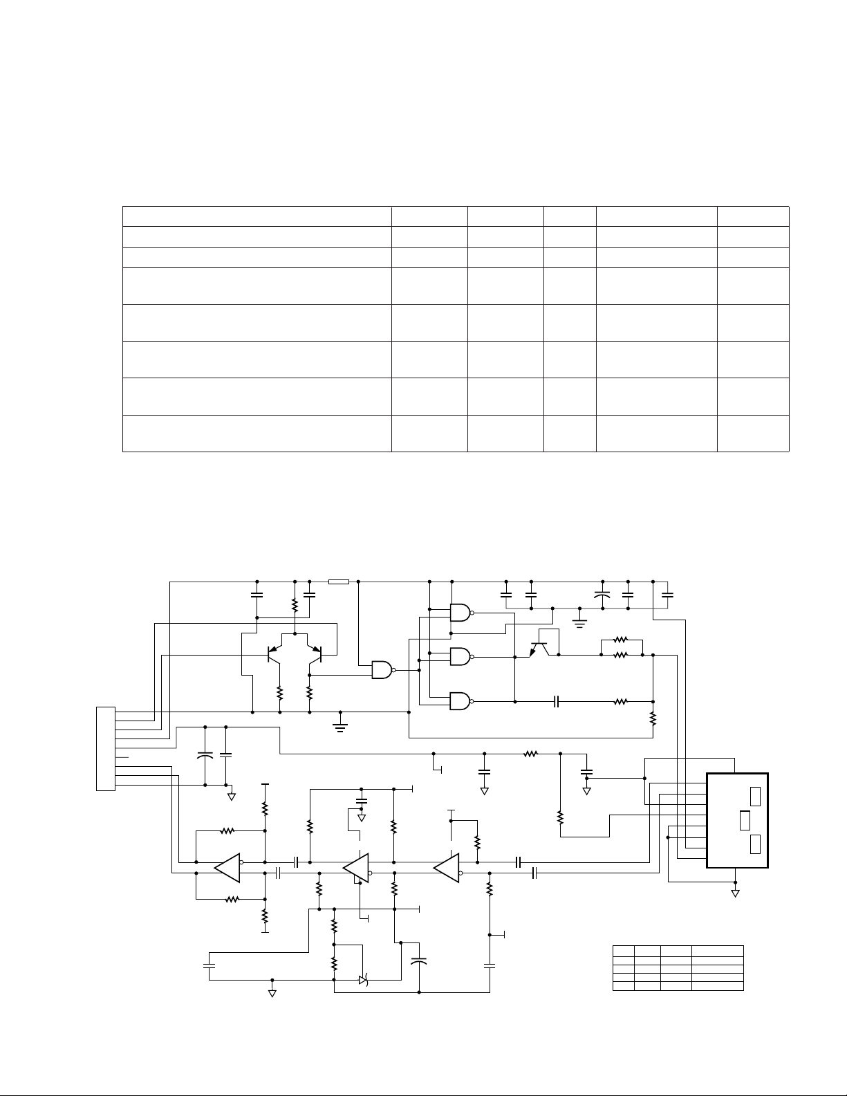
Figure 1. Transmitter and Receiver Application Circuit with +5 V ECL Inputs and Outputs.
168
Page 5

120 Ω 120 Ω
+5 V ECL
SERIAL DATA
SOURCE
0.1 µF
+5 V ECL
SERIAL DATA
RECEIVER
+
5 V
–
82 Ω
82 Ω
120 Ω 120 Ω
10 µF
+
+
0.1 µF
10 µF 0.1 µF
0.1 µF
4.7 µH
82 Ω
82 Ω
4.7 µH
4.7 µH
9 TX V
8 TD
7 TD
6 TX V
5 RX V
4
3 RD
2 RD
1 R
X VEE
EE
CC
CC
FIBER-OPTIC
TRANSCEIVER
SHOWN IN
FIGURE 1
Figure 2. Recommended Power Supply Filter and +5 V ECL Signal Terminations
for the Transmitter and Receiver Application Circuit of Figure 1.
200
150
100
50
AVERAGE POWER – µW
0
20 40 80 100
0
AVERAGE
MODULATED
POWER
AVERAGE POWER,
50% DUTY CYCLE
60
DUTY CYCLE – %
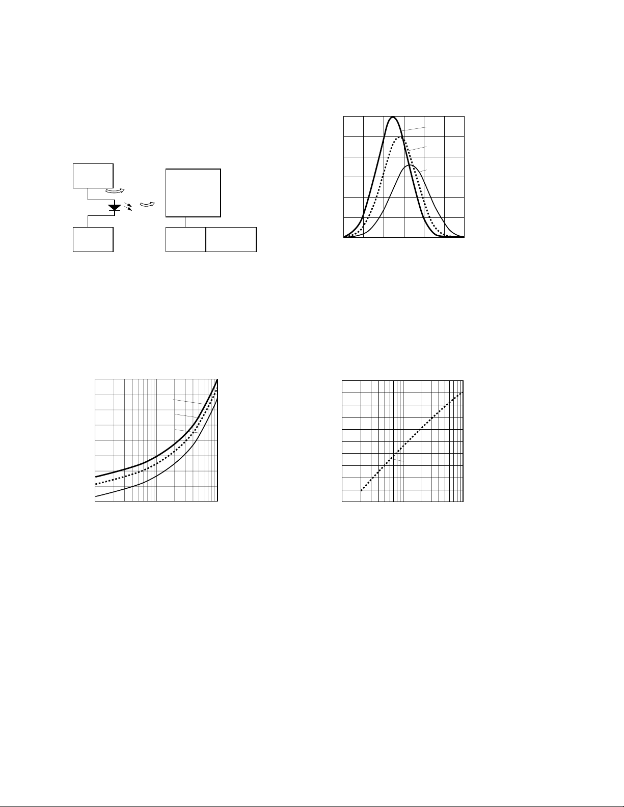
Figure 3. Average Modulated Power.
21
19
17
15
13
11
OPTICAL POWER BUDGET –dB
9
10
30 50
POF
HCS
9070 130 150
110
DATA RATE – MBd
Figure 4. Typical Optical Power
Budget vs. Data Rate.
169
Page 6

125 Megabaud Fiber Optic Link Transmitter/Receiver
Description
The HFBR-5527 incorporates a
650 nm LED, a PIN photodiode,
and transimpedance preamplifier.
The 650 nm LED is suitable for
use with current peaking to
decrease optical response time
and can be used with the PIN
preamplifier to build an optical
transceiver that can be operated
at signaling rates from 1 to 125
MBd over POF or HCS® fiber. The
receivers convert a received
optical signal to an analog output
voltage. Follow-on circuitry can
optimize link performance for a
variety of distance and data rate
requirements. Electrical
bandwidth greater than 65 MHz
allows design of high speed data
links with plastic or hard clad
silica optical fiber.
RX OUT
RX GND
RX GND
RX V
CC
GND
GND
ANODE
CATHODE
CASE
GND
10
1
2
3
4
5
6
7
8
9
CASE
GND
Absolute Maximum Ratings
Parameter Symbol Min. Max. Unit Reference
Storage Temperature T
Operating Temperature T
S
O
Lead Soldering Temperature 260 °C Note 1
Cycle Time
Transmitter High Level Forward I
F,H
Input Current ≥ 1 MHz
Transmitter Average Forward Input Current I
Transmitter Reverse Input Voltage V
Receiver Signal Pin Voltage V
Receiver Supply Voltage V
Receiver Output Current I
CAUTION: The small junction sizes inherent to the design of this component increase the component's susceptibility to damage from electrostatic discharge (ESD). It is advised that normal static precautions be taken in
handling and assembly of this component to prevent damage and/or degradation which may be induced by
ESD.
F,AV
R
O
CC
O
WARNING: WHEN VIEWED UNDER SOME CONDITIONS, THE OPTICAL PORT MAY
EXPOSE THE EYE BEYOND THE MAXIMUM PERMISSIBLE EXPOSURE RECOMMENDED
IN ANSI Z136.2, 1993. UNDER MOST VIEWING CONDITIONS THERE IS NO EYE HAZARD.
-40 +85 °C
-40 +70 °C
10 s
120 mA 50% Duty Cycle
60 mA
3V
-0.5 V
CC
-0.5 6.0 V
25 mA
V
170
Page 7

HFBR-5527 Transmitter Electrical/Optical Characteristics 0 to 70°C, unless otherwise stated.
Parameter Symbol Min. Typ.
Transmitter Output Optical P
T
-9.5 -7.0 -4.8 dBm I
Power, 1 mm POF -10.4 -4.3 0-70°C
Transmitter Output Optical P
Power, 200 µm HCS
®
Output Optical Power ∆P
T
T
Temperature Coefficient ∆T
Peak Emission Wavelength λ
PK
640 650 660 nm
Peak Wavelength ∆λ 0.12 nm/°C
Temperature Coefficient ∆T
Spectral Width FWHM 21 nm Full Width,
Forward Voltage V
Forward Voltage ∆V
F
1.8 2.0 2.4 V IF = 60 mA
F
Temperature Coefficient ∆T
Transmitter Numerical NA 0.5
Aperture
Thermal Resistance, θ
jc
Junction to Case
Reverse Input Breakdown V
BR
3.0 13 V I
Voltage
Diode Capacitance C
Unpeaked Optical Rise t
O
r
Time, 10% - 90% f = 100 kHz Note 5
Unpeaked Optical Fall t
f
Time, 90% - 10% f = 100 kHz Note 5
[2]
Max. Unit Condition Note
= 30 mA, 25°C Note 3
F,dc
-13.0 -10.5 dBm I
= 60 mA, 25°C Note 3
F,dc
-10.0 0-70°C
-0.02 dB/°C
Half Maximum
-1.8 mV/°C
140 °C/W Note 4
= -10 µA
F,dc
60 pF VF = 0 V,
f = 1 MHz
12 ns IF = 60 mA Figure 5
9nsI
= 60 mA Figure 5
F
Notes:
1. 1.6 mm below seating plane.
2. Typical data is at 25°C.
3. Optical Power measured at the end of 0.5 meter of 1 mm diameter plastic or 200 µm diameter hard clad silica optical fiber with a large
area detector.
4. Typical value measured from junction to PC board solder joint.
5. Optical rise and fall times can be reduced with the appropriate driver circuit.
6. Pins 9 and 10 are primarily for mounting and retaining purposes, but are electrically connected with conductive housing; pins 5 and 6
are electrically unconnected. It is recommended that pins 5, 6, 9, and 10 all be connected to Rx ground to reduce coupling of
electrical noise.
7. Refer to the Versatile Link Family Fiber Optic Cable and Connectors Technical Data Sheet for cable connector options for 1 mm
plastic optical fiber and 200 µm HCS fiber.
8. The LED current peaking necessary for high frequency circuit design contributes to electromagnetic interference (EMI). Care must be
taken in circuit board layout to minimize emissions for compliance with governmental EMI emissions regulations.
171
Page 8
HP8082A
PULSE
GENERATOR
50 OHM
LOAD
RESISTOR
BCP MODEL 300
500 MHz
BANDWIDTH
SILICON
AVALANCHE
PHOTODIODE
HP54002A
50 OHM BNC
INPUT POD
HP54100A
OSCILLOSCOPE
1.2
1.0
0.8
0.6
0.4
0.2
NORMALIZED SPECTRAL OUTPUT POWER
0
630 650 670 680
620
640
WAVELENGTH (nm)
0° C
25° C
70° C
660
Figure 5. Test Circuit for Measuring
Unpeaked Rise and Fall Times.
2.4
0° C
2.2
2.0
1.8
– FORWARD VOLTAGE – V
F
V
1.6
1
I
– TRANSMITTER DRIVE CURRENT (mA)
F,DC
25° C
70° C
10 100
Figure 7. Typical Forward Voltage vs.
Drive Current.
Figure 6. Typical Spectra Normalized
to the 25°C Peak.
+5
0
-5
-10
-15
– NORMALIZED OUTPUT POWER – dB
T
P
-20
1
I
– TRANSMITTER DRIVE CURRENT (mA)
F,DC
25° C
10 100
50
Figure 8. Typical Normalized Output
Optical Power vs. Drive Current with
the Drive Circuit in Figure 1
Recommended Application Circuit.
172
Page 9

HFBR-5527 Receiver Electrical/Optical Characteristics 0 to 70°C; 5.25 V ≥ V
(see Figure 1, Note 2).
Parameter Symbol Min. Typ. Max. Unit Test Condition Note
AC Responsivity 1 mm POF R
AC Responsivity 200 µm HCS R
RMS Output Noise V
Equivalent Optical Noise Input P
P,POF
P,HCS
NO
N,RMS
Power, RMS - 1 mm POF
Equivalent Optical Noise Input P
N,RMS
Power, RMS - 200 µm HCS
Peak Input Optical Power - P
R
1 mm POF -6.4 dBm 2 ns PWD
Peak Input Optical Power - P
R
200 µm HCS -9.4 dBm 2 ns PWD
Output Impedance Z
DC Output Voltage V
Supply Current I
O
O
CC
Electrical Bandwidth BW
Bandwidth * Rise Time 0.41 Hz * s
Electrical Rise Time, 10-90% t
Electrical Fall Time, 90-10% t
r
f
Pulse Width Distortion PWD 0.4 1.0 ns PR = -10 dBm Note 7
Overshoot 4 % PR = -10 dBm Note 8
1.7 3.9 6.5 mV/µW 650 nm Note 4
4.5 7.9 11.5 mV/µW
0.46 0.69 mV
-39 -36 dBm Note 5
-42 -40 dBm Note 5
30 Ω 50 MHz Note 4
0.8 1.8 2.6 V PR = 0 µW
915mA
E
65 125 MHz -3 dB electrical
3.3 6.3 ns PR = -10 dBm
3.3 6.3 ns PR = -10 dBm
≥ 4.75 V; power supply must be filtered
CC
RMS
Note 5
-5.8 dBm 5 ns PWD Note 6
-8.8 dBm 5 ns PWD Note 6
peak
peak
peak
peak
Notes:
1. 1.6 mm below seating plane.
2. The signal output is an emitter follower, which does not reject noise in the power supply. The power supply must be filtered as in
Figure 9.
3. Typical data are at 25°C and VCC = +5 Vdc.
4. Pin 1 should be ac coupled to a load ≥ 510 Ω with load capacitance less than 5 pF.
5. Measured with a 3 pole Bessel filter with a 75 MHz, -3 dB bandwidth. No modulation appled to Tx.
6. The maximum Peak Input Optical Power is the level at which the Pulse Width Distortion is guaranteed to be less than the PWD listed
under Test Condition. P
designing links up to 125 MBd (for both POF and HCS input conditions).
7. 10 ns pulse width, 50% duty cycle, at the 50% amplitude point of the waveform.
8. Percent overshoot is defined at:
9. Pins 9 and 10 are primarily for mounting and retaining purposes, but are electrically connected with the conductive housing. Pins 5
and 6 are electrically unconnected. It is recommended that pins 5 and 6 be connected to Rx ground to reduce coupling of electrical
noise. Refer to Figure 1. The connections between pins 1 and 2 of the HFBR-5527 and pins 13 and 12 of the MC10H116 should be
adjacent and nearly the same length to maximize the common mode rejection of the MC10H116 to eliminate cross talk between the
transmitter and receiver.
10. If there is no input optical power to the receiver (no transmitted signal) electrical noise can result in false triggering of the receiver.
In typical applications, data encoding and error detection prevent random triggering from being interpreted as valid data.
is given for PWD = 5 ns for designing links at ≤ 50 MBd operation, and also for PWD = 2 ns for
R,Max
(VPK - V
–––––––––––– × 100%
V
100%
100%
)
173
Page 10

V
CC
4.7 Ω
0.1 µF 0.47 µF
4.7 Ω
4
RECEIVER
9 10 2.3
Figure 9. Recommended Power Supply Filter Circuit.
The HFBR-5527 is typically used
to construct 125 MBd digital
fiber-optic receivers which use
the same +5 volt power supply
that powers the host system’s
microprocessors, CMOS logic, or
TTL logic. To build a digital
receiver, the analog HFBR-5527
component must be connected to
a post amplifier and a comparator. This post amplifier plus
comparator function is commonly
known as a quantizer. The 0 V
common and +5 V power supply
connections for the HFBR-5527
and quantizer must be isolated
from the host system’s power and
ground planes by a low pass
filter. This recommended low pass
RX
1
ANALOG
OUTPUT
filter assures that the electrical
noise normally present in the
host system’s digital logic power
supply will not reduce the
sensitivity of fiber-optic receivers
implemented with the
HFBR-5527. The quantizer and
power supply filter circuits
recommended for use with the
HFBR-5527 are shown in
Figure 7 of HP Application
Note 1066. For optimum
performance, the HFBR-5527
should be used with the same
quantizer and power supply
filters recommended for use with
HP’s HFBR-15X7 and
HFBR-25X6 components. To
maximize immunity to electrical
noise, pins 3, 9, and 10 of the
HFBR-5527 should be connected
to filtered receiver common. For
best common mode noise
rejection, the connections
between pins 1 and 2 of the
HFBR-5527 and the quantizer’s
differential input should be of
equal length, and the components
in both traces should be placed to
achieve symmetry. The preceding
recommendations minimize the
cross talk between the fiber-optic
transmitter and receiver. These
recommendations also improve
the fiber-optic receiver’s
immunity to environmental noise
and the host system’s electrical
noise.
174
Page 11

BIAS & FILTER
CIRCUITS
Figure 10. Simplified Receiver Schematic.
5.0
mA
900 pF
4 POSITIVE
SUPPLY
RX
1
ANALOG
OUTPUT
2.3
GROUND
Figure 11. Typical Pulse Width
Distortion vs. Peak Input Power.
Figure 12. Typical Output Spectral
Noise Density vs. Frequency.
Figure 13. Typical Rise and Fall Time
vs. Temperature.
175
Page 12

HFBR-5527 Mechanical Dimensions
16
SINGAPORE
hp XXXX
HFBR-5527
22
10.16
8.5
5.76
3.5
2.54 2.11
ALL DIMENSIONS IN MILLIMETERS (INCHES).
ALL DIMENSIONS ± 0.25 mm
UNLESS OTHERWISE SPECIFIED.
0.3
4.39
5.85
0.51
0.64
Printed Circuit Board Layout Dimensions
20.3
1.11 2.54 (0.100)
1.01 (0.040) DIA.
12345678
4.39
4.4
1
20
176
9 10
TOP VIEW
ELECTRICAL PIN FUNCTIONS
PIN NO.
1
RX OUT
2
RX GND
3
RX GND
4
RX V
5
6
7
8
9
10
*NO INTERNAL CONNECTION
CC
TX GND*
TX GND*
ANODE
CATHODE
CASE GND
CASE GND
CAUTION:
THIS PACKAGE IS MADE
OF CONDUCTIVE PLASTIC.
PLEASE TAKE THIS INTO
ACCOUNT WHEN
INCORPORATING THIS
PACKAGE INTO INTRINSICALLY
SAFE APPLICATIONS.
NOTE:
DIMENSIONS IN MILLIMETERS
AND (INCHES).
 Loading...