

Datasheet HFBR-5113FDA, HFBR-5112FDS, HFBR-5112FDN, HFBR-5112FDM, HFBR-5112FDB Datasheet (HP)
...Page 1

92
Low Cost, Industry Standard
FDDI MIC Transceivers
Technical Data
HFBR-5111 (2x11)
HFBR-5112 (Narrow 1x13)
HFBR-5113 (Standard 1x13)
Features
• Full Compliance with the
FDDI PMD Standard
• Full Compliance with the
Optical Performance
Requirements of the ATM
100 Mbps Physical Layer
• Full Compliance with the
Optical Performance
Requirements of the Fast
Ethernet Physical Layer
• Multisourced Package Style
with:
- 2x11 or 1x13 Pin
Configuration
- MIC Receptacle
- Field Changeable Keying
• Wave Solder and Aqueous
Wash Process Compatible
Package
• Internal Shielding for Low
EMI Emissions and High
EMI Immunity
• Single +5V Power Supply
• Shifted ECL Logic Interface
Directly Compatible with
FDDI PHY Circuits
• Manufactured in an ISO
9001 Certified Facility
Applications
• FDDI Concentrators,
Bridges, Routers, and
Network Interface Cards
• 100 Mbps ATM Interfaces
• Fast Ethernet Interfaces
• Point-to-Point Data
Communications
• Replaces DLX2012-FD and
DLX2020-FD Model
Transceivers
Description
The HFBR-511X family of transceivers from Hewlett-Packard
consists of high performance,
cost effective modules for optical
data communication applications
at the 100 Mbps/125 MBd rate.
The transceivers feature full
compliance with the Fiber
Distributed Data Interface (FDDI)
Physical Media Dependent (PMD)
standard. This standard has been
approved as an International
Standard, ISO/IEC 9314-3, and
an American National Standard,
ANSI X3.166 - 1990. The HFBR5111 represents the 2x11
package style. The “2x11”
denotes two rows of eleven pins.
The HFBR-5112 and HFBR-5113
represent the Narrow and
Standard 1x13 package styles,
respectively. The “1x13” denotes
one row of thirteen pins.
The modules are designed for 50
or 62.5 µm core multimode
optical fiber and operate at a
nominal wavelength of 1300 nm.
Each transceiver incorporates
our high-performance, reliable,
long-wavelength optical devices
and proven circuit technology to
give long life and consistent
performance.
The transceivers are optimized
for 125 MBd operation but can be
used over a wide range of signal
rates. The transceivers are
guaranteed to meet FDDI PMD
specifications when used within
the operating conditions specified
in this document.
These HFBR-511X Series transceivers are also useful for both
ATM 100 Mbps interfaces and
Fast Ethernet 100 Base-FX
interfaces. The ATM Forum UserNetwork Interface (UNI)
Standard, Version 3.0, defines the
Physical Layer for 100 Mbps
Multimode Fiber Interface for
ATM in Section 2.3 to be the
5964-9019E (2/96)
Page 2

93
FDDI PMD standard. Likewise,
the Fast Ethernet Alliance defines
the Physical Layer for the 100
Base-FX Version of IEEE 802.3u
to be the FDDI PMD standard.
Hewlett-Packard also provides
several other FDDI products
compliant with the FDDI Low
Cost Fiber (LCF) -PMD and
Single Mode (SM) -PMD
standards. These products are
available with ST, SC, and FC
connector styles. They are
available in the 1x9 transceiver
and 14- and 16-pin transmitter/
receiver package styles for those
designs that require these
alternate configurations. Contact
your Hewlett-Packard sales
representative for information on
these alternative FDDI products.
Transmitter Section
The transmitter section of the
HFBR-511X Series utilizes a 1300
nm surface emitting InGaAsP
LED. The LED is packaged in the
optical subassembly portion of
the transmitter section. It is dccoupled to a custom IC which
converts differential-input, PECL
logic signals, ECL referenced
(shifted) to a +5 V power supply,
into an analog LED drive current.
Receiver Section
The receiver section of the
HFBR-511X Series utilizes an
InGaAs PIN photodiode coupled
to a custom silicon transimpedance preamplifier IC. They are
packaged in the optical subassembly portion of the receiver.
The PIN/preamplifier combination is ac-coupled to a custom
quantizer IC which provides the
final pulse shaping for the logic
output and the Signal Detect
function. Both the Data and
Signal Detect outputs are
differential. Also, both Data and
Signal Detect outputs are PECL
compatible, ECL referenced
(shifted) to a +5 V power supply.
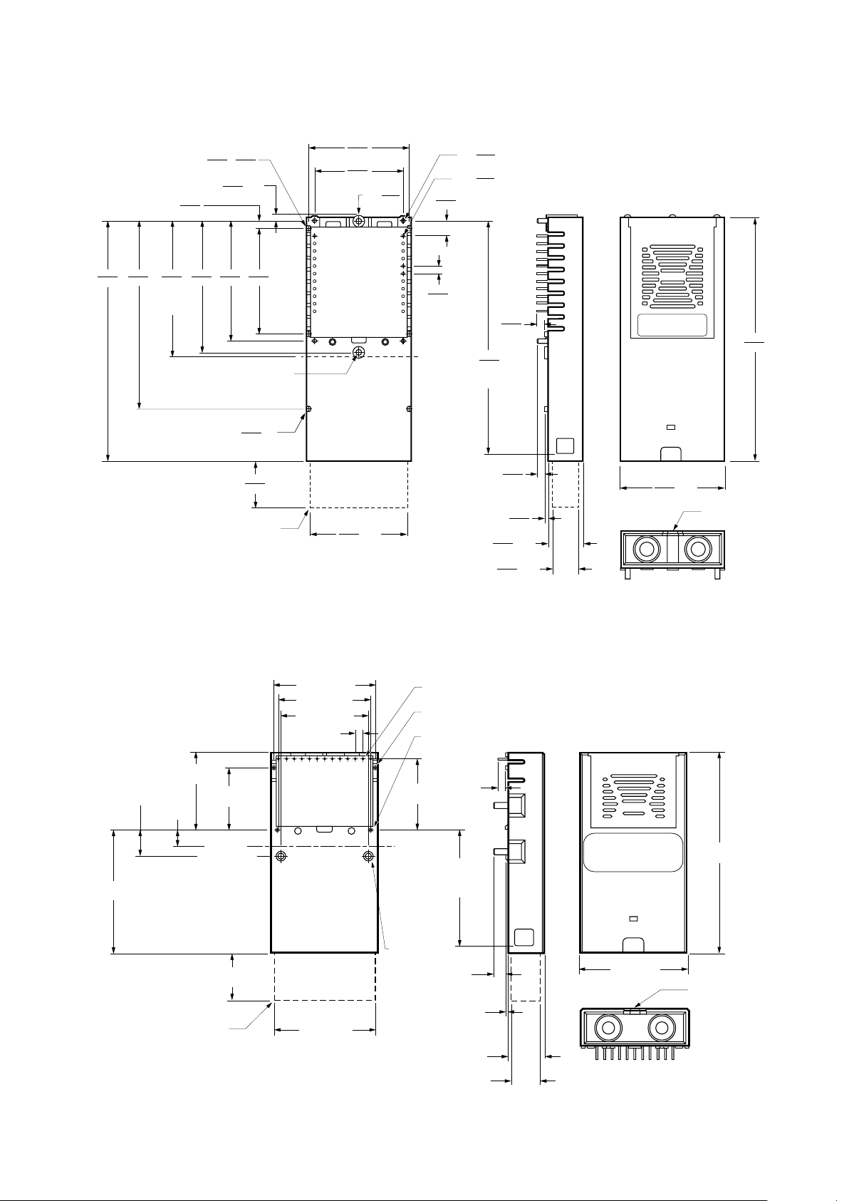
Package
The overall package concept for
the HP transceiver consists of the
following basic elements: two
optical subassemblies, an
electrical subassembly, and the
housing with full compliance to
the FDDI PMD standard. A block
diagram is illustrated in Figure 1.
The package outline drawings
and pin-outs are shown in Figures
2 and 3. These are compliant with
the industry standard 2x11 and
1x13 pin configurations.
The optical subassemblies utilize
a high-volume assembly process
together with low-cost lens
elements which result in a costeffective building block.
The electrical subassemblies
consist of a high-volume, multilayer printed circuit board on
which the IC chips and various
surface-mounted passive circuit
elements are attached.
Each transceiver package
includes internal shields for the
electrical and optical subassemblies to ensure low EMI emissions
and high immunity to external
EMI fields.
The outer housings including the
MIC receptacles are molded of
filled non-conductive plastic to
provide mechanical strength and
electrical isolation. The solder
posts of each package design are
isolated from the circuit design of
the transceiver and do not require
connection to a ground plane on
the circuit board.
Each transceiver is attached to its
printed circuit boards with the
2x11 or 1x13 signal pins and the
solder posts which exit the
bottom of the housing. The solder
posts provide the primary
mechanical strength to withstand
the loads imposed on the
transceiver when mating with
MIC-connectored fiber cables.
Application Information
The Applications Engineering
group of the Optical Communication Division is available to assist
you with the technical under
Figure 1. HFBR-5111/-5112/-5113 Block Diagram.
DATA OUT
SIGNAL
DETECT OUT
DATA IN
ELECTRICAL SUBASSEMBLY
QUANTIZER IC
DRIVER IC
TOP VIEW
PIN PHOTODIODE
OPTICAL
SUBASSEMBLIES
LED
PREAMP
IC
DIFFERENTIAL
DIFFERENTIAL
DIFFERENTIAL
MEDIA INTERFACE CONNECTOR
RECEPTACLE
Page 3
94
H
39.94
(1.533)
LATCH
POINTS
33.02
(1.300)
MAX.
2.54
(0.100)
TYP.
34.46 (1.357)
29.00 (1.142)
13X ∅
LEADS
0.48
(0.019)
2X ∅
1.00
(0.039)
2X ∅
SOLDER POSTS
1.52
(0.060)
22.86
(0.900)
19.99
(0.787)
24.86
(0.979)
OPTICAL
REFERENCE
PLANE
5.79
(0.228)
9.14
(0.360)
41.30
(1.626)
16.00
(0.630)
MAX.
2X ∅
3.00
(0.118)
PLUG – REF.
66.16
(2.605)
MAX.
35.80
(1.409)
MAX.
2.95
(0.116)
3.68
(0.145)
0.80
(0.031)
11.87
(0.467)
9.40
(0.370)
MAX.
MAX.
FDDI KEY
LOCATION
PART NUMBER
DATE CODE
COUNTRY OF ORIGIN
30.48 (1.200)
ø
NOTES:
1. ALL DIMENSIONS ARE MILLIMETERS OVER INCHES.
2. ALL DIMENSIONS ARE NOMINAL UNLESS OTHERWISE SPECIFIED.
3. THE LEADS ARE TIN-LEAD PLATED PHOSPHOR BRONZE.
4. THE POSTS ARE TIN-LEAD PLATED BRASS.
5. THE HOUSING IS GLASS FIBER FILLED BLACK POLYETHERIMIDE.
6. THE MODULE IS SHOWN WITHOUT THE FIELD KEY INSTALLED.
H
PART NUMBER
DATE CODE
COUNTRY OF ORIGIN
35.80
1.409
MAX.
82.5
3.248
MAX.
2.54
0.100
TYP.
5.08
0.200
78.87
3.105
LATCH
POINTS
2.95
0.116
2.95
0.116
0.85
0.034
11.87
0.467
9.40
0.370
MAX.
MAX.
FDDI KEY
LOCATION
33.02
1.300
MAX.
35.56
1.400
40.64
1.600
44.45
1.750
45.72
1.800
OPTICAL
REFERENCE
PLANE
81.32
3.202
63.5
2.500
1.52
0.060
SQ.2X
16.00
0.630
MAX.
PLUG – REF.
ACCEPTS SELF TAPPING
2X – M2X0.4 SCREW FOR
OPTIONAL MOUNTING
1.91
0.075
MAX.
2.54
0.100
1.22
0.050
X4X
1.52
0.060
3.80
0.150
2X
34.34
1.352
30.48
1.200
ø
1.50
0.060
4X SOLDER POSTS
ø
0.48
0.019
22X LEADS
Figure 2(a). HFBR-5111 Outline Drawing.
Figure 2(b). HFBR-5112 Outline Drawing.
Page 4
95
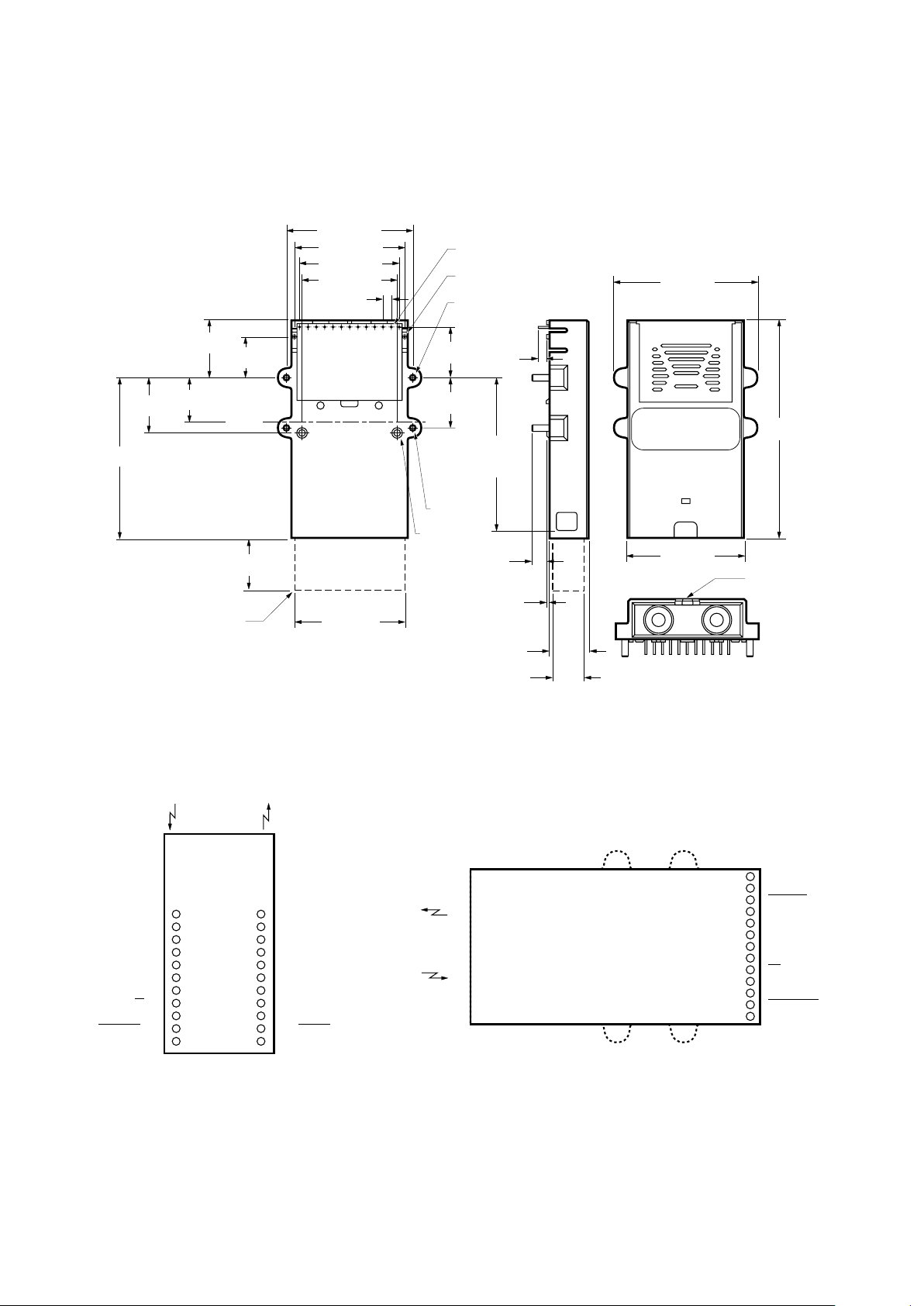
Figure 2(c). HFBR-5113 Outline Drawing.
H
46.56
(1.833)
LATCH
POINTS
33.02
(1.300)
MAX.
2.54
(0.100)
TYP.
38.10 (1.500)
34.46 (1.357)
29.00 (1.142)
13X ∅
LEADS
0.48
(0.019)
2X ∅
1.00
(0.039)
4X ∅
SOLDER POSTS
2.00
(0.079)
15.24
(0.600)
15.24
(0.600)
12.37
(0.487)
17.24
(0.679)
OPTICAL
REFERENCE
PLANE
13.41
(0.528)
16.76
(0.660)
48.92
(1.926)
16.00
(0.630)
MAX.
4X R
2.80
(0.110)
2X ∅
3.00
(0.118)
PLUG – REF.
66.16
(2.605)
MAX.
43.80
(1.724)
MAX.
35.80
(1.409)
MAX.
2.95
(0.116)
4.50
(0.177)
0.80
(0.031)
11.87
(0.467)
9.40
(0.370)
MAX.
MAX.
NOTES:
1. ALL DIMENSIONS ARE MILLIMETERS OVER (INCHES).
2. ALL DIMENSIONS ARE NOMINAL UNLESS OTHERWISE SPECIFIED.
3. THE LEADS ARE TIN-LEAD PLATED PHOSPHOR BRONZE.
4. THE POSTS ARE TIN-LEAD PLATED BRASS.
5. THE HOUSING IS GLASS FIBER FILLED BLACK POLYETHERIMIDE.
6. THE MODULE IS SHOWN WITHOUT THE FIELD KEY INSTALLED.
FDDI KEY
LOCATION
PART NUMBER
DATE CODE
COUNTRY OF ORIGIN
30.48 (1.200)
GND 1
NC 2
V
CC
3
V
CC
4
GND 5
GND 6
SD 7
SD 8
V
CC
9
DATA OUT 10
DATA OUT 11
22 GND
21 V
CC
20 V
CC
19 V
CC
18 V
CC
17 GND
16 GND
15 GND
14 V
BB
13 DATA IN
12 DATA IN
TOP VIEW
Figure 3. Pin Assignments.
(a) HFBR-5111
(b) HFBR-5112/-5113
TOP VIEW
GND
V
B
DATA IN
DATA IN
TX V
CC
GND
GND
RX V
CC
SD
SD
DATA OUT
DATA OUT
GND
13
1
Page 5
96
Hewlett-Packard LED technology
has produced 1300 nm LED
devices with lower aging characteristics than normally associated
with these technologies in the
industry. The industry convention
is 1.5 dB aging for 1300 nm
LEDs, however HP 1300 nm
LEDs will experience less than 1
dB of aging over normal commercial equipment mission life
periods. Contact your HewlettPackard sales representative for
additional details.
Figure 4 was generated with a
Hewlett-Packard fiber-optic link
model containing the current
industry conventions for fiber
cable specifications and the FDDI
PMD optical parameters. These
parameters are reflected in the
guaranteed performance of the
transceiver specifications in this
data sheet. This same model has
been used extensively in the ANSI
and IEEE committees, including
the ANSI X3T9.5 committee, to
establish the optical performance
requirements for various fiberoptic interface standards. The
cable parameters used come from
the ISO/IEC JTC1/SC 25/WG3
Generic Cabling for Customer
Premises per DIS 11801
document and the EIA/TIA-568-A
Commercial Building Telecommunications Cabling Standard per
SP-2840.
Transceiver Signaling
Operating Rate Range and
BER Performance
For purposes of definition, the
symbol rate (Baud), also called
signaling rate, is the reciprocal of
the symbol time. Data rate (bits/
sec) is the symbol rate divided by
the encoding factor used to
encode the data (symbols/bit).
When used in FDDI 100 Mbps
applications, the performance of
the 1300 nm transceivers is
guaranteed over the signaling
rate of 10 MBd to 125 MBd to the
full conditions listed in the
individual product specification
tables.
The transceivers may be used for
other applications at signaling
rates outside of the 10 MBd to
125 MBd range with some
penalty in the link optical power
budget primarily caused by a
reduction of receiver sensitivity.
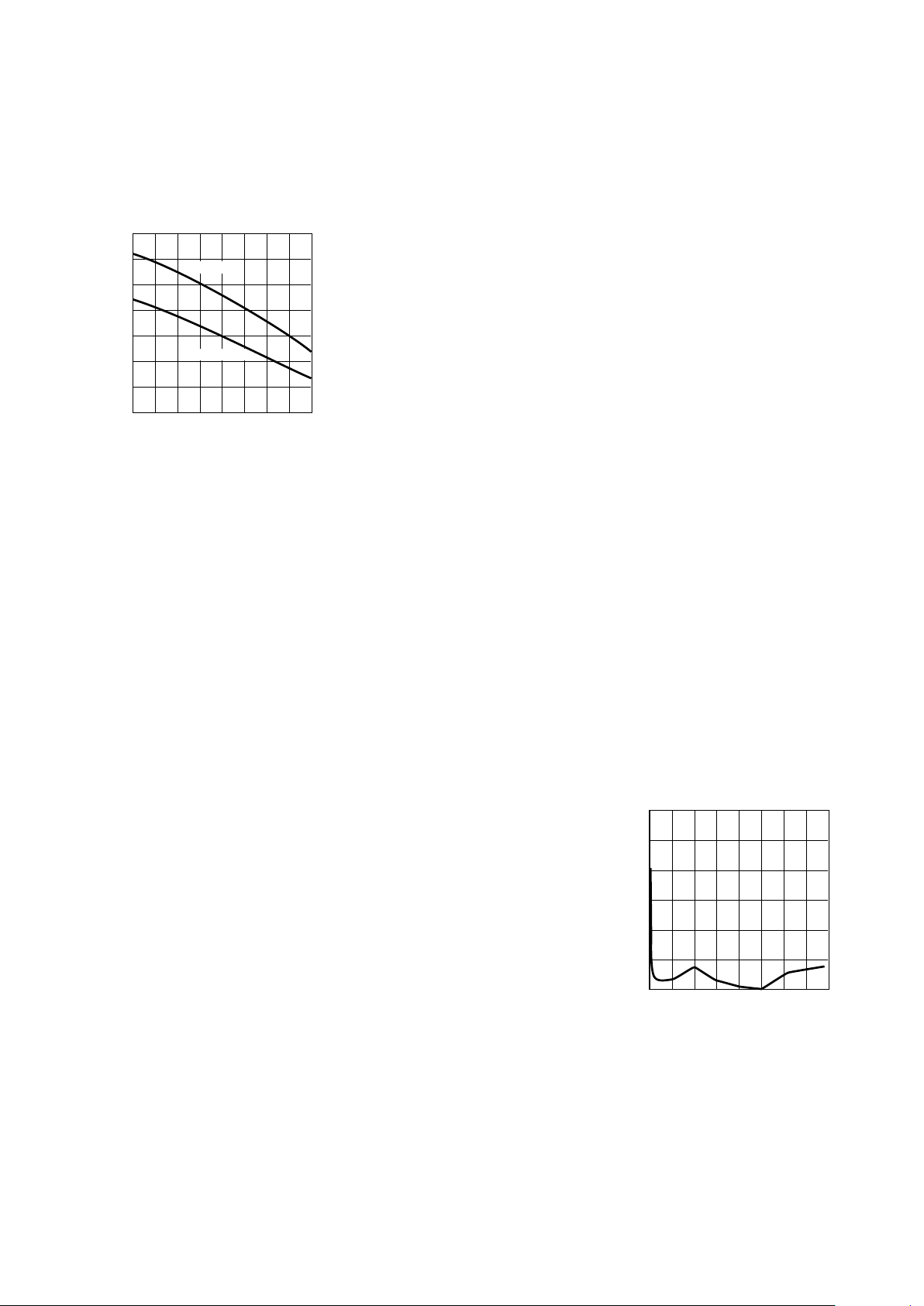
Figure 5 gives an indication of
the typical performance of these
1300 nm products at different
rates.
These transceivers can also be
used for applications which
require different bit error rate
(BER) performance. Figure 6
illustrates the typical trade-off
between link BER and the
receiver’s input optical power
level.
Figure 5. Transceiver Relative
Optical Power Budget at Constant
BER vs. Signaling Rate.
TRANSCEIVER RELATIVE OPTICAL POWER
BUDGET AT CONSTANT BER – dB
0 200
3.0
0
SIGNAL RATE (MBd)
25 75 100 125
2.5
2.0
1.5
1.0
175
0.5
50 150
CONDITIONS:
1. PRBS 2
7
-1
2. DATA SAMPLED AT CENTER OF DATA SYMBOL.
3. BER = 10
-6
4. TA = 25° C
5. V
CC
= 5 V
dc
6. INPUT OPTICAL RISE/FALL TIMES = 1.0/2.1 ns.
standing and design trade-offs
associated with this transceiver.
You can contact them through
your Hewlett-Packard sales
representative.
The following information is
provided to answer some of the
most common questions about
the use of these parts.
Transceiver Optical Power
Budget versus Link Length
The Optical Power Budget (OPB)
is the available optical power for
a fiber-optic link to accommodate
fiber cable losses plus losses due
to in-line connectors, splices,
optical switches, and to provide
margin for link aging and
unplanned losses due to cable
plant reconfiguration or repair.
Figure 4 illustrates the predicted
OPB associated with the transceivers specified in this data
sheet at the Beginning of Life
(BOL). This curve represents the
attenuation and chromatic plus
modal dispersion losses
associated with the 62.5/125 µm
and 50/125 µm fiber cables only.
The area under the curve
represents the remaining OPB at
any link length, which is available
for overcoming non-fiber cable
related losses.
Figure 4. Optical Power Budget at
BOL vs. Fiber Optic Cable Length.
OPB – OPTICAL POWER BUDGET – dB
0 4.0
14
0
FIBER OPTIC CABLE LENGTH – km
0.5 1.5 2.0 2.5
12
10
8
4
3.5
2
1.0 3.0
6
62.5/125 µm
50/125 µm
Page 6

97
E1 of Annex E. They represent
the worst-case jitter contribution
that the transceivers are allowed
to make to the overall system
jitter without violating the Annex
E allocation example. In practice,
the typical contribution of the HP
transceiver is well below the
maximum amount.
Recommended Handling
Precautions
It is advised that normal static
precautions be taken in the
handling and assembly of these
transceivers to prevent damage
which may be induced by
electrostatic discharge (ESD).
The HFBR-511X Series meets
MIL-STD-883C Method 3015.4
Class 2.
Care should be taken to avoid
shorting the receiver Data or
Signal Detect outputs directly to
ground without proper currentlimiting impedance.
Solder and Wash Process
Compatibility
Each transceiver is delivered with
a protective port plug inserted
into the MIC receptacle. This port
process plug protects the optical
subassembly during wave solder
and aqueous wash processing and
acts as a dust cover during
shipping. The port process plugs
have been tested up to and found
to withstand 110 psi and 190°F.
These transceivers are
compatible with either industry
standard wave- or hand-solder
processes.
Shipping Container
Each transceiver is packaged in a
shipping container designed to
protect it from mechanical and
ESD damage during shipment or
storage.
Board Layout–Decoupling
Circuit and Ground Planes
It is important to take care in the
layout of your circuit board to
achieve optimum performance
from these transceivers. Figure 7
provides a good example of
schematics for decoupling
circuits that work well with this
product. It is further recommended that a contiguous ground
plane be provided in the circuit
board directly under the
transceiver to provide a low
inductance ground for signal
return current. This recommendation is in keeping with good high
frequency board layout practices.
Board Layout–Hole Pattern
The hole pattern shown in Figure
8 for the 2x11 package style
complies with the pin sizes
specified by the multisource
agreement. Hole patterns are also
provided for the Standard and
Narrow 1x13 package styles.
These drawings can be used as a
guide in the mechanical layout of
your circuit board.
Board Layout–Art Work
The Applications Engineering
group has developed Gerber file
artwork for various fiber optic
transceiver layouts. Contact your
local Hewlett-Packard sales
representative for details.
Regulatory Compliance
These transceiver products are
intended to enable commercial
system designers to develop
equipment that complies with the
various international regulations
governing certification of Information Technology Equipment.
See Table 1 for details. Additional
information is available from your
Hewlett-Packard sales
representative.
Figure 6. Bit Error Rate vs. Relative
Receiver Input Optical Power.
BIT ERROR RATE
-6 4
1 x 10
-2
RELATIVE INPUT OPTICAL POWER – dB
-4 2-2
0
1 x 10
-4
1 x 10
-6
1 x 10
-8
2.5 x 10
-10
1 x 10
-11
CONDITIONS:
1. 125 MBd
2. PRBS 2
7
-1
3. CENTER OF SYMBOL SAMPLING.
4. T
A
= 25° C
5. V
CC
= 5 V
dc
6. INPUT OPTICAL RISE/FALL TIMES = 1.0/2.1 ns.
1 x 10
-12
1 x 10
-7
1 x 10
-5
1 x 10
-3
CENTER OF
SYMBOL
Transceiver Jitter
Performance
The Hewlett-Packard 1300 nm
transceivers are designed to
operate per the system jitter
allocations stated in Table E1 of
Annex E of the FDDI PMD
standard.
The HP 1300 nm transmitters will
tolerate the worst-case input
electrical jitter allowed in the
table without violating the worstcase output optical jitter
requirement of Sections 8.1
Active Output Interface of the
FDDI PMD standard.
The HP 1300 nm receivers will
tolerate the worst-case input
optical jitter allowed in Section
8.2 Active Input Interface of the
FDDI PMD standard without
violating the worst-case output
electrical jitter allowed in the
Table E1 of the Annex E.
The jitter specifications stated in
the following 1300 nm transceiver specification table are
derived from the values in Table
Page 7

98
1
2
3
4
5
6
7
8
9
10
11
GND
V
CC
V
CC
V
CC
V
CC
GND
GND
GND
V
BB
DATA IN
DATA IN
TOP VIEW
GND
NC
V
CC
V
CC
GND
GND
SD
SD
V
CC
DATA OUT
DATA OUT
GND GND
GND GND
22
21
20
19
18
17
16
15
14
13
12
DATA
DATA
DATA
DATA
SIGNAL DETECT
SIGNAL DETECT
R11
130
R12
130
R3
130
R4
130
R9
82
R10
82
R182R2
82
C5
0.1
L1
1
C1
20
V
CC
Rx Tx
L2
1
C3
10
C4
0.1
R6
82
R5
82
R8
130
R7
130
C2
0.1
(a) HFBR-5111
Figure 7. Recommended Decoupling Circuit Diagram.
(b) HFBR-5112/-5113
TOP
VIEW
GND
V
B
DATA IN
DATA IN
TX V
CC
GND
GND
RX V
CC
SD
SD
DATA OUT
DATA OUT
GND
13
12
11
10
9
8
7
6
5
4
3
2
1
C1
20
C5
0.1
DATA IN
DATA IN
V
CC
SD
SD
DATA OUT
DATA OUT
R6
82
R5
82
R8
130
R7
130
C4
0.1
L2
1
R3
130
R1
82
R4
130
R2
82
R12
130
R10
82
R11
130
R9
82
C3
10
C2
0.1
L1
1
NOTES:
1. PLACE TERMINATION RESISTORS NEAR INPUT DATA PINS OF TRANSCEIVER AND PHY DEVICES.
2. MAKE DIFFERENTIAL SIGNAL PATHS SHORT AND OF THE SAME LENGTH WITH EQUAL TERMINATIONS TO V
CC
– 2 VOLTS.
3. SIGNAL TRACES SHOULD BE 50 Ω TRANSMISSION LINES: MICROSTRIP (OR STRIPLINE). USE GROUND PLANE
(OR MULTI-LAYER) PRINTED CIRCUIT BOARD FOR BEST HIGH FREQUENCY PERFORMANCE.
4. RESISTORS IN Ω. CAPACITORS IN MICROFARADS. INDUCTORS IN MICROHENRIES.
5. USE HIGH-FREQUENCY MONOLITHIC CERAMIC BYPASS CAPACITORS AND LOW SERIES DC RESISTANCE INDUCTORS.
FERRITE INDUCTORS CAN BE USED.
LOCATE POWER SUPPLY FILTER COMPONENTS CLOSE TO FIBER-OPTIC DEVICES.
6. CAUTION: DO NOT DIRECTLY CONNECT FIBER-OPTIC MODULE PECL OUTPUTS (DATA, DATA, SIGNAL DETECT, SIGNAL DETECT)
TO GROUND WITHOUT PROPER CURRENT LIMITING IMPEDANCE.
7. DEVICE GROUND PINS SHOULD BE DIRECTLY AND INDIVIDUALLY CONNECTED TO GROUND.
8. DEVICE SOLDER POSTS SHOULD BE DIRECTLY CONNECTED TO PCB FOR OPTIMUM MECHANICAL SUPPORT.
Page 8

99
22.86
0.900
30.48
1.200
1.93 ± 0.15
0.076 ± 0.006
2X
φ
φ 0.000
MA
1.00 ± 0.15
0.039 ± 0.006
13X
φ
φ 0.000
MA
–A–
NOTES:
1. DIMENSIONS ARE IN MILLIMETERS OVER INCHES.
2. DIMENSIONS PER ANSI Y 14.5 M.
2.54
0.100
TYP
(a) HFBR-5111
40.64
1.600
30.48
1.200
1.93 ± 0.15
0.076 ± 0.006
4X
φ
φ 0.000
MA
1.04 ± 0.15
0.041 ± 0.006
22X
φ
φ 0.000
MA
–A–
2.54
0.100
TYP
5.08
0.200
NOTES:
1. DIMENSIONS ARE IN MILLIMETERS OVER INCHES.
2. DIMENSIONS PER ANSI Y 14.5 M.
Figure 8. Board Layout–Hole Pattern.
(c) HFBR-5113
(b) HFBR-5112
19.05 19.05
5.08 MIN.
30.48
15.24
2.54 x 12
3.81
4 – ∅ 2.4
∅ 0.1 A BM
13 – ∅ 1.0
∅ 0.1 M
± 0.1
A
B
UNIT: mm
NOTES:
1. TOLERANCE ± 0.05 mm, UNLESS OTHERWISE SPECIFIED.
2. SOLDER POSTS SHOULD BE CONNECTED TO PCB FOR OPTIMUM MECHANICAL SUPPORT.
± 0.1
Page 9

100
Electrostatic Discharge
There are two design cases in
which immunity to ESD damage
is important.
The first is during handling of the
transceiver prior to mounting it
on the circuit board. It is
important to use normal ESD
handling precautions for ESDsensitive devices. These precautions include using grounded
wrist straps, work benches, and
floor mats in ESD-controlled
areas.
The second case to consider is
static discharges to the exterior
of the equipment chassis containing the transceiver parts. To
the extent that the MIC connector
is exposed to the outside of the
equipment chassis, it may be
subject to whatever ESD system
level test criteria that the
equipment is intended to meet.
Electromagnetic Interference
(EMI)
Most equipment designs utilizing
these high speed transceivers
from Hewlett-Packard will be
required to meet the requirements of FCC in the United
States, CENELEC EN55022
(CISPR 22) in Europe and VCCI
in Japan. Hence, the HFBR-511X
Series of fiber optic transceivers
meet the regulatory requirements
listed in Table 1.
Immunity
Equipment utilizing these
transceivers will be subject to
radio-frequency electromagnetic
fields in some environments.
These transceivers have a high
immunity to such fields. The
internal construction of the
HFBR-511X Series is similar to
that of the HFBR-510X/-520X
series. Therefore, for additional
information regarding EMI susceptibility, ESD, and conducted
noise testing procedures and
results, please refer to Application Note 1075, Testing and
Measuring Electromagnetic
Compatibility Performance of
the HFBR-510X/-520X Fiber
Optic Transceivers.
Flammability Rating
The housing material of the
HFBR-5111/-5112/-5113 transceiver has been approved for UL
flammability rating of 94V-0
under General Electric’s UL file
number E121562 and similarly
under CSA file number LS88480.
Transceiver Reliability and
Performance Qualification
Data
As with all HP components, the
HFBR-511X series transceivers
undergo extensive HewlettPackard reliability and performance qualification testing. Details
are available from your HewlettPackard sales representative.
These transceivers are manufactured at the Hewlett-Packard
Singapore location which is an
ISO 9001 certified facility.
Ordering Information
The Hewlett-Packard FDDI
transceivers are available
packaged with or without key
inserts per Table 2. The key
inserts are colored-coded plastic
parts with an identifying key
letter molded into the top surface
of each key.
The HFBR-5111/-5112/-5113
products are available through
the Hewlett-Packard Component
Field Sales Offices and
Authorized Distributors
worldwide.
Table 1. Regulatory Compliance Table
Feature Test Method Performance
Electrostatic Discharge MIL-STD-883C Meets Class 2 (2000 to 3999 Volts)
(ESD) to the Electrical Pins Method 3015.4 Withstands up to 2200 V applied between
electrical pins.
Electrostatic Discharge Variation of IEC 801-2 Typically withstand at least 25 kV without
(ESD) to the MIC Receptacle damage when the MIC Receptacle is contacted
by a Human Body Model probe.
Electromagnetic Interference FCC Class B Typically provide a 13 dB margin to the noted
(EMC) CENELEC CEN55022 standard limits when tested at a certified
Class B (CISPR 22B) test range with the transceiver mounted to a
VCCI Class 2 circuit card without a chassis enclosure.
Immunity Variation of IEC 801-3 Typically show no measurable effect from a
10 V/m field swept from 10 to 450 MHz
applied to the transceiver when mounted to a
circuit card without a chassis enclosure.
Page 10

101
Table 2. Ordering Information
Part Number Description
Transceivers
HFBR-5111 2x11 Transceiver with a set of 4 key inserts (A, B, M, and S)
HFBR-5111 Option FDA 2x11 Transceiver with A-key installed
HFBR-5111 Option FDB 2x11 Transceiver with B-key installed
HFBR-5111 Option FDM 2x11 Transceiver with M-key installed
HFBR-5111 Option FDS 2x11 Transceiver with S-key installed
HFBR-5111 Option FDN 2x11 Transceiver with no key inserts included
HFBR-5112 Narrow 1x13 Transceiver with a set of 4 key inserts (A, B, M, and S)
HFBR-5112 Option FDA Narrow 1x13 Transceiver with A-key intalled
HFBR-5112 Option FDB Narrow 1x13 Transceiver with B-key installed
HFBR-5112 Option FDM Narrow 1x13 Transceiver with M-key installed
HFBR-5112 Option FDS Narrow 1x13 Transceiver with S-key installed
HFBR-5112 Option FDN Narrow 1x13 Transceiver with no key inserts included
HFBR-5113 Standard 1x13 Transceiver with a set of 4 key inserts (A, B, M, and S)
HFBR-5113 Option FDA Standard 1x13 Transceiver with A-key intalled
HFBR-5113 Option FDB Standard 1x13 Transceiver with B-key installed
HFBR-5113 Option FDM Standard 1x13 Transceiver with M-key installed
HFBR-5113 Option FDS Standard 1x13 Transceiver with S-key installed
HFBR-5113 Option FDN Standard 1x13 Transceiver with no key inserts included
Accessories
HFBR-5001 One Port Process Plug
HFBR-5198 One Bag of 4 Key Inserts (A,B,M, and S)
Figure 9. Transmitter Output Optical
Spectral Width (FWHM) vs.
Transmitter Output Optical Center
Wavelength and Rise/Fall Times.
1380
200
100
λC – TRANSMITTER OUTPUT OPTICAL
CENTER WAVELENGTH –nm
1200 1300 1320
180
160
140
120
13601340
∆λ – TRANSMITTER OUTPUT OPTICAL
SPECTRAL WIDTH (FWHM) –nm
t
r/f
– TRANSMITTER
OUTPUT OPTICAL
RISE/FALL TIMES – ns
1.5
2.0
3.0
3.5
2.5
3.0
3.5
HFBR-511X FDDI TRANSMITTER TEST RESULTS
OF λ
C
, ∆λ AND t
r/f
ARE CORRELATED AND
COMPLY WITH THE ALLOWED SPECTRAL WIDTH
AS A FUNCTION OF CENTER WAVELENGTH FOR
VARIOUS RISE AND FALL TIMES.
Page 11

102
40 ± 0.7
10.0
4.850
1.525
0.525
5.6
100% TIME
INTERVAL
± 0.725
± 0.725
4.40
1.975
0.075
0.50
0.025
-0.025
0.0
-0.05
0.10
10.0
5.6
1.525
0.525
4.850
80 ± 500 ppm
4.40
1.975
0.075
0.90
1.025
1.25
TIME – ns
0% TIME
INTERVAL
1.00
0.975
RELATIVE AMPLITUDE
THE HFBR-511X OUTPUT OPTICAL PULSE SHAPE FITS WITHIN THE BOUNDARIES
OF THE PULSE ENVELOPE FOR RISE AND FALL TIME MEASUREMENTS.
Figure 10. Output Optical Pulse Envelope.
Figure 11. Relative Input Optical
Power vs. Eye Sampling Time
Position.
Figure 12. Signal Detect Thresholds and Timing.
-31.0 dBm
-45.0 dBm
SIGNAL – DETECT (ON)
SIGNAL – DETECT (OFF)
AS – MAX
INPUT OPTICAL POWER
(> 1.5 dB STEP INCREASE)
INPUT OPTICAL POWER
(> 4.0 dB STEP DECREASE)
P
O
= MAX (PS OR -45.0 dBm)
(P
S
= INPUT POWER FOR BER < 102)
MIN (P
O
+ 4.0 dB OR -31.0 dBm)
P
A (PO
+ 1.5 dB
< P
A
< -31.0 dBm)
OPTICAL POWER
TIME
SIGNAL
DETECT
OUTPUT
AS – MAX — MAXIMUM ACQUISITION TIME (SIGNAL).
AS – MAX IS THE MAXIMUM SIGNAL – DETECT ASSERTION TIME FOR THE STATION.
AS – MAX SHALL NOT EXCEED 100.0 µs. THE DEFAULT VALUE OF AS – MAX IS 100.0 µs.
ANS – MAX — MAXIMUM ACQUISITION TIME (NO SIGNAL).
ANS – MAX IS THE MAXIMUM SIGNAL – DETECT DEASSERTION TIME FOR THE STATION.
ANS – MAX SHALL NOT EXCEED 350 µs. THE DEFAULT VALUE OF AS – MAX IS 350 µs.
ANS – MAX
RELATIVE INPUT OPTICAL POWER – dB
-4 4
0
EYE SAMPLING TIME POSITION (ns)
-3 -1 0 1
5
4
3
2
3
1
-2 2
CONDITIONS:
1.T
A
= 25° C
2. V
CC
= 5 Vdc
3. INPUT OPTICAL RISE/FALL TIMES = 1.0/2.1 ns.
4. INPUT OPTICAL POWER IS NORMALIZED TO
CENTER OF DATA SYMBOL.
5. NOTE 20 AND 21 APPLY.
2.5 x 10
-10
BER
1.0 x 10
-12
BER
Page 12

103
Absolute Maximum Ratings
Parameter Symbol Min. Typ. Max. Unit Reference
Storage Temperature T
S
-40 100 °C
Lead Soldering Temperature T
SOLD
260 °C
Lead Soldering Time t
SOLD
10 sec.
Supply Voltage V
CC
-0.5 7.0 V
Data Input Voltage V
I
-0.5 V
CC
V
Differential Input Voltage V
D
1.4 V Note 1
Output Current I
O
50 mA
Recommended Operating Conditions
Parameter Symbol Min. Typ. Max. Unit Reference
Ambient Operating Temperature T
A
070°C
Supply Voltage V
CC
4.75 5.25 V
Data Input Voltage – Low VIL - V
CC
-1.810 -1.475 V
Data Input Voltage – High VIH - V
CC
-1.165 -0.880 V
Data and Signal Detect Output Load R
L
50 Ω Note 2
Signaling Rate f
S
10 125 MBd Note 3
Figures 5, 6
Transmitter Electrical Characteristics
(TA = 0°C to 70°C, VCC = 4.75 V to 5.25 V)
Parameter Symbol Min. Typ. Max. Unit Reference
Supply Current I
CC
145 185 mA Note 4
Power Dissipation P
DISS
0.76 0.97 W
Threshold Voltage VBB - V
CC
-1.42 -1.3 -1.24 V Note 5
Data Input Current – Low I
IL
-350 0 µA
Data Input Current – High I
IH
14 350 µA
Receiver Electrical Characteristics
(TA = 0°C to 70°C, VCC = 4.75 V to 5.25 V)
Parameter Symbol Min. Typ. Max. Unit Reference
Supply Current I
CC
102 165 mA Note 6
Power Dissipation P
DISS
0.3 0.5 W Note 7
Data Output Voltage – Low VOL – V
CC
-1.840 -1.620 V Note 8
Data Output Voltage – High VOH – V
CC
-1.045 -0.880 V Note 8
Data Output Rise Time t
r
0.35 2.2 ns Note 9
Data Output Fall Time t
f
0.35 2.2 ns Note 9
Signal Detect Output Voltage – Low VOL – V
CC
-1.840 -1.620 V Note 8
Signal Detect Output Voltage – High VOH – V
CC
-1.045 -0.880 V Note 8
Signal Detect Output Rise Time t
r
0.35 2.2 ns Note 9
Signal Detect Output Fall Time t
f
0.35 2.2 ns Note 9
Page 13

104
Transmitter Optical Characteristics
(TA = 0°C to 70°C, VCC = 4.75 V to 5.25 V)
Parameter Symbol Min. Typ. Max. Unit Reference
Output Optical Power BOL P
O
-19 -16.8 -14 dBm avg. Note 13
62.5/125 µm, NA = 0.275 Fiber EOL -20
Output Optical Power BOL P
O
-22.5 -20.3 -14 dBm avg. Note 13
50/1255 µm, NA = 0.20 Fiber EOL -23.5
Optical Extinction Ratio 0.001 0.03 % Note 14
-50 -35 dB
Output Optical Power at Logic “0” State PO (“0”) -45 dBm avg. Note 15
Center Wavelength λ
C
1270 1308 1380 nm Note 16
Figure 9
Spectral Width – FWHM ∆λ 137 170 nm Note 16
Figure 9
Optical Rise Time t
r
0.6 1.0 3.0 ns Note 16, 17
Figure 9, 10
Optical Fall Time t
f
0.6 2.1 3.0 ns Note 16, 17
Figure 9, 10
Duty Cycle Distortion Contributed DCD 0.02 0.6 ns p-p Note 18
by the Transmitter
Data Dependent Jitter Contributed DDJ 0.02 0.6 ns p-p Note 19
by the Transmitter
Random Jitter Contributed by the RJ 0 0.69 ns p-p Note 20
Transmitter
Receiver Optical Characteristics
(TA = 0°C to 70°C, VCC = 4.75 V to 5.25 V)
Parameter Symbol Min. Typ. Max. Unit Reference
Input Optical Power Minimum at P
IN Min.
(W) -33.5 -31 dBm avg. Note 21
Window Edge Figure 11
Input Optical Power Minimum P
IN Min.
(C) -34.5 -31.8 dBm avg. Note 22
at Eye Center Figure 11
Input Optical Power Maximum P
IN Max.
-14 -11.8 dBm avg. Note 21
Operating Wavelength λ 1270 1380 nm
Duty Cycle Distortion Contributed DCD 0.02 0.4 ns p-p Note 10
by the Receiver
Data Dependent Jitter Contributed DDJ 0.35 1.0 ns p-p Note 11
by the Receiver
Random Jitter Contributed by the RJ 1.0 2.14 ns p-p Note 12
Receiver
Signal Detect – Asserted P
A
PD + 1.5 dB -33 dBm avg. Note 23, 24
Figure 12
Signal Detect – Deasserted P
D
-45 dBm avg. Note 25, 26
Figure 12
Signal Detect – Hysteresis PA - P
D
1.5 2.4 dB Figure 12
Signal Detect Assert Time (off to on) AS_Max 0 55 100 µs Note 23, 24
Figure 12
Signal Detect Deassert Time (on to off) ANS_Max 0 110 350 µs Note 25, 26
Figure 12
Page 14

105
Notes:
1. This is the maximum voltage that can
be applied across the Differential
Transmitter Data Inputs to prevent
damage to the input ESD protection
circuit.
2. The outputs are terminated with 50 Ω
connected to VCC-2V.
3. The specified signaling rate of
10 MBd to 125 MBd guarantees
operation of the transmitter and
receiver link to the full conditions
listed in the FDDI Physical Layer
Medium Dependent standard.
Specifically, the link bit error ratio
will be equal to or better than
2.5 x 10
-10
for any valid FDDI
pattern. The transmitter section of
the link is capable of dc to 125 MBd.
The receiver is internally ac-coupled
which limits the lower signaling rate
to 10 MBd. For purposes of
definition, the symbol rate (Baud),
also called signaling rate, fs, is the
reciprocal of the shortest symbol
time. Data rate (bits/sec) is the
symbol rate divided by the encoding
factor used to encode the data
(symbols/bit).
4. The power supply current needed to
operate the transmitter is provided to
differential ECL circuitry. This
circuitry maintains a nearly constant
current flow from the power supply.
Constant current operation helps to
prevent unwanted electrical noise
from being generated and conducted
or emitted to neighboring circuitry.
5. This value is measured with an output
load RL = 10 kΩ.
6. This value is measured with the outputs terminated into 50 Ω connected
to VCC- 2 V and an Input Optical
Power level of -14 dBm average.
7. The power dissipation value is the
power dissipated in the receiver
itself. Power dissipation is calculated
as the sum of the products of supply
voltage and currents, minus the sum
of the products of the output voltages
and currents.
8. This value is measured with respect to
VCC with the output terminated into
50 Ω connected to VCC-2V.
9. The output rise and fall times are
measured between 20% and 80%
levels with the output connected to
VCC- 2 V through 50 Ω.
10. Duty Cycle Distortion contributed by
the receiver is measured at the 50%
threshold using an IDLE Line State,
125 MBd (62.5 MHz square-wave),
input signal. The input optical power
level is -20 dBm average. See
Application Information - Transmitter
Jitter Section for further information.
11. Data Dependent Jitter contributed by
the receiver is specified with the
FDDI DDJ test pattern described in
the FDDI PMD Annex A.5. The input
optical power level is -20 dBm
average. See Application Information
- Transmitter Jitter Section for
further information.
12. Random Jitter contributed by the
receiver is specified with an IDLE
Line State, 125 Mbd (62.5 MHz
square-wave), input signal. The input
optical power level is at maximum
“P
IN Min.
(W).” See Application
Information - Transmitter Jitter
Section for further information.
13. These optical power values are
measured with the following
conditions:
• The Beginning of Life (BOL) to the
End of Life (EOL) optical power
degradation is typically 1.5 dB per
the industry convention for long
wavelength LEDs. The actual
degradation observed in HewlettPackard’s 1300 nm LED products
is < 1 dB, as specified in this data
sheet.
• Over the specified operation voltage
and temperature ranges.
• With HALT Line State, (12.5 MHz
square-wave), input signal.
• At the end of one meter of noted
optical fiber with cladding modes
removed.
The average power value can be
converted to a peak power value by
adding 3 dB. Higher output optical
power transmitters are available on
special request.
14. The Extinction Ratio is a measure of
the modulation depth of the optical
signal. The data “0” output optical
power is compared to the data “1”
peak output optical power and
expressed as a percentage. With the
transmitter driven by a HALT Line
State (12.5 MHz square-wave) signal,
the average optical power is
measured. The data “1” peak power is
then calculated by adding 3 dB to the
measured average optical power. The
data “0” output optical power is
found by measuring the optical power
when the transmitter is driven by a
logic “0” input. The extinction ratio is
the ratio of the optical power at the
“0” level compared to the optical
power at the “1” level expressed as a
percentage or in decibels.
15. The transmitter provides compliance
with the need for Transmit_Disable
commands from the FDDI SMT layer
by providing an Output Optical
Power level of < -45 dBm average in
response to a logic “0” input. This
specification applies to either
62.5/125 µm or 50/125 µm fiber
cables.
16. This parameter complies with the
FDDI PMD requirements for the
tradeoffs between center wavelength,
spectral width, and rise/fall times
shown in Figure 9.
17. This parameter complies with the
optical pulse envelope from the FDDI
PMD shown in Figure 10. The optical
rise and fall times are measured from
10% to 90% when the transmitter is
driven by the FDDI HALT Line State
(12.5 MHz square-wave) input signal.
18. Duty Cycle Distortion contributed by
the transmitter is measured at a 50%
threshold using an IDLE Line State,
125 MBd (62.5 MHz square-wave),
input signal. See Application Information – Transceiver Jitter Performance
Section of this data sheet for further
details.
19. Data Dependent Jitter contributed by
the transmitter is specified with the
FDDI test pattern described in FDDI
PMD Annex A.5. See Application
Information – Transceiver Jitter
Performance Section of this data
sheet for further details.
20. Random Jitter contributed by the
transmitter is specified with an IDLE
Line State, 1256 MBd (62.5 MHz
square-wave), input signal. See
Application Information – Transceiver Jitter Performance Section of
this data sheet for further details.
21. This specification is intended to indicate the performance of the receiver
section of the transceiver when Input
Optical Power signal characteristics
are present per the following
definitions. The Input Optical Power
dynamic range from the minimum
level (with a window time-width) to
the maximum level is the range over
which the receiver is guaranteed to
provide output data with a Bit Error
Ratio (BER) better than or equal to
2.5 x 10
-10
.
• At the Beginning of Life (BOL).
• Over the specified operation
temperature and voltage ranges.
Page 15

106
• Input symbol pattern is the FDDI
test pattern defined in FDDI PMD
Annex A.5 with 4B/5B NRZI
encoded data that contains a duty
cycle base-line wander effect of
50 kHz. This sequence causes a
near worst case condition for intersymbol interference.
• Receiver data window time-width is
2.13 ns or greater and centered at
mid-symbol. This worst case
window time-width is the minimum
allowed eye-opening presented to
the FDDI PHY PM_Data indication
input (PHY input) per the example
in FDDI PMD Annex E. This
minimum window time-width of
2.13 ns is based upon the worst
case FDDI PMD Active Input
Interface optical conditions for
peak-to-peak DCD (1.0 ns), DDJ
(1.2 ns) and RJ (0.76 ns)
presented to the receiver.
To test a receiver with the worst case
FDDI PMD Active Input jitter condition requires exacting control over
DCD, DDJ and RJ jitter components
that is difficult to implement with
production test equipment. The
receiver can be equivalently tested to
the worst case FDDI PMD input jitter
conditions and meet the minimum
output data window time-width of
2.13 ns. This is accomplished by
using a nearly ideal input optical
signal (no DCD, insignificant DDJ
and RJ) and measuring for a wider
window time-width of 4.6 ns. This is
possible due to the cumulative effect
of jitter components through their
superposition (DCD and DDJ are
directly additive and RJ components
are rms additive). Specifically, when
a nearly ideal input optical test signal
is used and the maximum receiver
peak-to-peak jitter contributions of
DCD (0.4 ns), DDJ (1.0 ns), and RJ
(2.14 ns) exist, the minimum window
time-width becomes 8.0 ns -0.4 ns -
1.0 ns - 2.14 ns = 4.46 ns, or
conservatively 4.6 ns. This wider
window time-width of 4.6 ns
guarantees the FDDI PMD Annex E
minimum window time-width of
2.13 ns under worst case input jitter
conditions to the Hewlett-Packard
receiver.
• Transmitter operating with an IDLE
Line State pattern, 125 MBd
(62.5 MHz square-wave), input
signal to simulate any cross-talk
present between the transmitter
and receiver sections of the
transmitter.
22. All conditions of Note 21 apply
except that the measurement is made
at the center of the symbol with no
window time-width.
23. This value is measured during the
transition from low to high levels of
input optical power.
24. The Signal Detect output shall be
asserted within 100 µs after a step
increase of the Input Optical Power.
The step will be from a low Input
Optical Power, ≤ -45 dBm, into the
range between greater than PA, and
-14 dBm. The BER of the receiver
output will be 10-2 or better during
the time, LS_Max (15 µs) after Signal
Detect has been asserted. See Figure
12 for more information.
25. This value is measured during the
transition from high to low levels of
input optical power. The maximum
value will occur when the input
optical power is either -45 dBm
average or when the input optical
power yields a BER of 10-2 or better,
whichever power is higher.
26. Signal detect output shall be deasserted
within 350 µs after a step decrease in
the Input Optical Power from a
level which is the lower of: -31 dBm
or PD + 4 dB (PD is the power level at
which signal detect was deasserted),
to a power level of -45 dBm or less.
This step decrease will have occurred
in less than 8 ns. The receiver output
will have a BER of 10-2 or better for a
period of 12 µs or until signal detect
is deasserted. The input data stream
is the Quiet Line State. Also, signal
detect will be deasserted within a
maximum of 350 µs after the BER of
the receiver output degrades above
10-2 for an input optical data stream
that decays with a negative ramp
function instead of a step function.
See Figure 12 for more information.
 Loading...