

Page 1
126
5965-9727E (5/97)
FDDI, 100 Mbps ATM, and
Fast Ethernet Transceivers
in Low Cost 1x9 Package Style
Technical Data
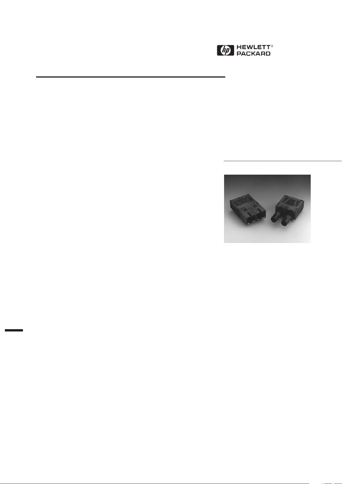
Description
The HFBR-5100 family of transceivers from Hewlett-Packard
provide the system designer with
products to implement a range of
FDDI and ATM (Asynchronous
Transfer Mode) designs at the
100 Mbps/125 MBd rate.
The transceivers are all supplied
in the new industry standard 1x9
SIP package style with either a
duplex SC or a duplex ST*
connector interface.
FDDI PMD, ATM and Fast
Ethernet 2000 m Backbone
Links
The HFBR-5103/-5103T are
1300 nm products with optical
performance compliant with the
FDDI PMD standard. The FDDI
PMD standard is ISO/IEC 9314-3:
1990 and ANSI X3.166 - 1990.
These transceivers for 2000 meter
multimode fiber backbones are
supplied in the small 1x9 duplex
SC or ST package style for those
designers who want to avoid the
larger MIC/R (Media Interface
Connector/Receptacle) defined in
the FDDI PMD standard.
Hewlett-Packard also provides
several other FDDI products
compliant with the PMD and SMPMD standards. These products
Features
• Full Compliance with the
Optical Performance
Requirements of the FDDI
PMD Standard
• Full Compliance with the
FDDI LCF-PMD Standard
• Full Compliance with the
Optical Performance
Requirements of the ATM
100 Mbps Physical Layer
• Full Compliance with the
Optical Performance
Requirements of
100 Base-FX Version of
IEEE 802.3u
• Very Low Cost 800 nm
Alternative with FDDI and
ATM Compliant Signaling
• Multisourced 1x9 Package
Style with Choice of Duplex
SC or Duplex ST*
Receptacle
• Wave Solder and Aqueous
Wash Process Compatible
• Manufactured in an ISO
9002 Certified Facility
Applications
• Multimode Fiber Backbone
Links
• Multimode Fiber Wiring
Closet to Desktop Links
• Very Low Cost Multimode
Fiber 800 nm Links from
Wiring Closet to Desktop
*ST is a registered trademark of AT&T Lightguide Cable Connectors.
HFBR-5103/-5103T
1300 nm 2000 m
HFBR-5104/-5104T
800 nm 500 m
HFBR-5105/-5105T
1300nm 500 m
are available with MIC/R, ST© and
FC connector styles. They are
available in the 1x13 and 2x11
transceiver and 16 pin
transmitter/receiver package
styles for those designs that
require these alternate
configurations.
The HFBR-5103/-5103T is also
useful for both ATM 100 Mbps
interfaces and Fast Ethernet 100
Base-FX interfaces. The ATM
Forum User-Network Interface
(UNI) Standard, Version 3.0,
defines the Physical Layer for
100 Mbps Multimode Fiber
Interface for ATM in Section 2.3
to be the FDDI PMD Standard.
Likewise, the Fast Ethernet
Alliance defines the Physical
Layer for 100 Base-FX for Fast
Ethernet to be the FDDI PMD
Standard.
Note: The “T” in the product numbers
indicates a transceiver with a duplex ST
connector receptacle.
Product numbers without a “T” indicate
transceivers with a duplex SC connector
receptacle.
Page 2
127
ATM applications for physical
layers other than 100 Mbps
Multimode Fiber Interface are
supported by Hewlett-Packard.
Products are available for both
the single mode and the multimode fiber SONET OC-3c
(STS-3c) ATM interfaces and the
155 Mbps/194 MBd multimode
fiber ATM interface as specified
in the ATM Forum UNI.
Contact your Hewlett-Packard
sales representative for information on these alternative FDDI
and ATM products.
Low Cost 500 m Desktop
Links
The HFBR-5105/-5105T are
1300 nm products which are fully
compliant with the requirements
of the FDDI LCF-PMD standard.
The FDDI LCF-PMD standard is
in the final approval stage as ISO/
IEC WD 9314-9 and ANSI LCFPMD Revision 1.3.
These multimode fiber transceivers can be used for 500 meter
backbone and desktop links for
FDDI, Fast Ethernet, or ATM 100
Mbps traffic.
The HFBR-5105 transceiver
utilizes the duplex SC connector
receptacle specified in the FDDI
LCF-PMD standard.
Alternative 800 nm Low Cost
500 m Desktop Links
The HFBR-5104/-5104T are very
low cost 800 nm alternative to
the HFBR-5105/-5105T for FDDI,
ATM or Fast Ethernet links from
the wiring closet to the desktop.
They comply with the performance requirements of the draft
FDDI LCF-PMD document as
translated by Hewlett-Packard to
the 800 nm wavelength. This
transceiver will transfer the full
range of FDDI signals at the
required 1x10
-12
Bit Error Rate
over distances up to 500 meters
using 62.5/125 µm multimode
fiber cables.
This product is intended for use
in cost sensitive applications
where the benefits of fiber optic
links are important.
Transmitter Sections
The transmitter sections of the
HFBR-5103 and HFBR-5105
series utilize 1300 nm Surface
Emitting InGaAsP LEDs and the
HFBR-5104 series uses a low cost
820 nm AlGaAs LED. These LEDs
are packaged in the optical
subassembly portion of the
transmitter section. They are
driven by a custom silicon IC
which converts differential PECL
logic signals, ECL referenced
(shifted) to a +5 Volt supply, into
an analog LED drive current.
Receiver Sections
The receiver sections of the
HFBR-5103 and HFBR-5105
series utilize InGaAs PIN photodiodes coupled to a custom
silicon transimpedance preamplifier IC. The HFBR-5104 series
uses the same preamplifier IC in
conjunction with an inexpensive
silicon PIN photodiode. These are
packaged in the optical subassembly portion of the receiver.
These PIN/preamplifier combinations are coupled to a custom
quantizer IC which provides the
final pulse shaping for the logic
output and the Signal Detect
function. The data output is differential. The signal detect output
is single-ended. Both data and
signal detect outputs are PECL
compatible, ECL referenced
(shifted) to a +5 Volt power
supply.
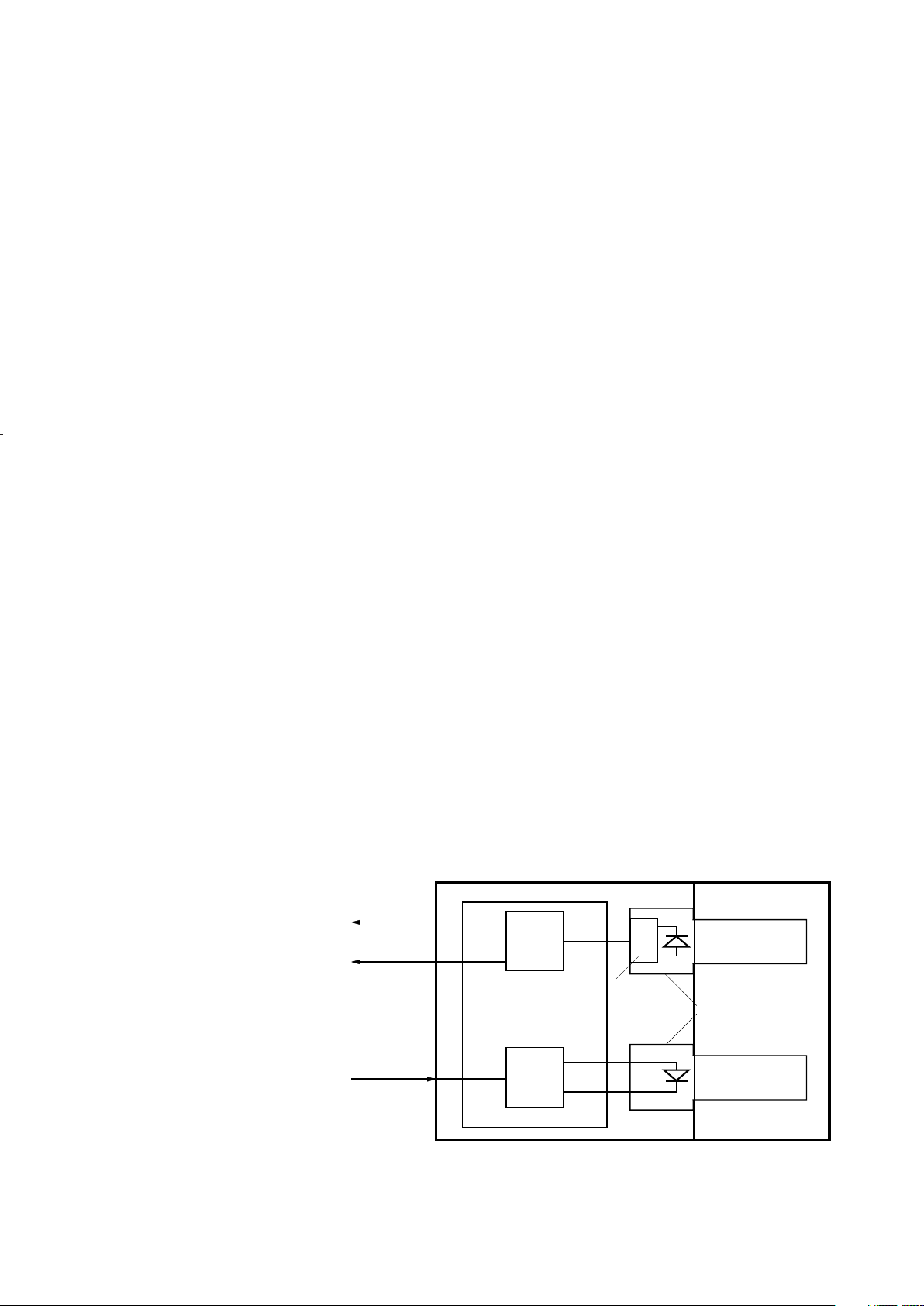
Package
The overall package concept for
the HP transceivers consists of
the following basic elements; two
optical subassemblies, an
electrical subassembly and the
housing as illustrated in Figure 1
and Figure 1a.
The package outline drawing and
pin out are shown in Figures 2,
2a and 3. The details of this
package outline and pin out are
compliant with the multisource
Figure 1. Block Diagram.
DATA OUT
SIGNAL
DETECT OUT
DATA IN
ELECTRICAL SUBASSEMBLY
QUANTIZER IC
DRIVER IC
TOP VIEW
PIN PHOTODIODE
DUPLEX SC
RECEPTACLE
OPTICAL
SUBASSEMBLIES
LED
PREAMP IC
DIFFERENTIAL
SINGLE-ENDED
DIFFERENTIAL
Page 3
128
DATA OUT
SIGNAL
DETECT OUT
DATA IN
ELECTRICAL SUBASSEMBLY
QUANTIZER IC
DRIVER IC
TOP VIEW
PIN PHOTODIODE
DUPLEX ST
RECEPTACLE
OPTICAL
SUBASSEMBLIES
LED
PREAMP IC
DIFFERENTIAL
SINGLE-ENDED
DIFFERENTIAL
Figure 1a. ST Block Diagram.
Figure 2. Package Outline Drawing.
39.12
(1.540)
MAX.
AREA
RESERVED
FOR
PROCESS
PLUG
12.70
(0.500)
25.40
(1.000)
MAX.
12.70
(0.500)
10.35
(0.407)
MAX.
+ 0.25
- 0.05
+ 0.010
- 0.002
3.30 ± 0.38
(0.130 ± 0.015)
2.92
(0.115)
18.52
(0.729)
4.14
(0.163)
20.32
(0.800)
[8x(2.54/.100)]
23.55
(0.927)
16.70
(0.657)
17.32
(0.682)
20.32
(0.800)
23.32
(0.918)
0.46
(0.018)
NOTE 1
(9x)ø
NOTE 1
0.87
(0.034)
23.24
(0.915)
15.88
(0.625)
NOTE 1: THE SOLDER POSTS AND ELECTRICAL PINS ARE PHOSPHOR BRONZE WITH TIN LEAD OVER NICKEL PLATING.
DIMENSIONS ARE IN MILLIMETERS (INCHES).
HFBR-5103 fig 2
1.27
(0.050
+ 0.08
- 0.05
+ 0.003
- 0.002
0.75
(0.030
)
)
H
HFBR-5XXX
DATE CODE (YYWW)
SINGAPORE
Page 4
129
Figure 3. Pin Out Diagram.
definition of the 1x9 SIP. The low
profile of the Hewlett-Packard
transceiver design complies with
the maximum height allowed for
the duplex SC connector over the
entire length of the package.
The optical subassemblies utilize
a high volume assembly process
together with low cost lens
elements which result in a cost
effective building block.
The electrical subassembly consists of a high volume multilayer
printed circuit board on which
the IC chips and various surface-
Figure 2a. ST Package Outline Drawing.
25.4
(1.000)
MAX.
24.8
(0.976)
42
(1.654)
MAX.
5.99
(0.236)
12.7
(0.500)
12.0
(0.471)
MAX.
0.5
(0.020)
3.3 ± 0.38
(0.130) (± 0.015)
+ 0.08
- 0.05
+ 0.003
- 0.002
+ 0.25
- 0.05
+ 0.010
- 0.002
20.32
± 0.38
(± 0.015)
HFBR-5103T
DATE CODE (YYWW)
SINGAPORE
3.2
(0.126)
2.6
(0.102)
φ
22.86
(0.900)
20.32
(0.800)
[(8x (2.54/0.100)]
17.4
(0.685)
21.4
(0.843)
20.32
(0.800)
3.6
(0.142)
1.3
(0.051)
23.38
(0.921)
18.62
(0.733)
NOTE 1: PHOSPHOR BRONZE IS THE BASE MATERIAL FOR THE POSTS & PINS
WITH TIN LEAD OVER NICKEL PLATING.
DIMENSIONS IN MILLIMETERS (INCHES).
(
(
(
(
0.46
(0.022)
NOTE 1
φ
1 = V
EE
2 = RD
3 = RD
4 = SD
5 = V
CC
6 = V
CC
7 = TD
8 = TD
9 = V
EE
TOP VIEW
N/C
N/C
Page 5
130
technologies in the industry. The
industry convention is 3 dB aging
for 800 nm and 1.5 dB aging for
1300 nm LEDs. The HP 1300 nm
LEDs will experience less than
1 dB of aging over normal commercial equipment mission life
periods. Contact your HewlettPackard sales representative for
additional details.
Figure 4 was generated with a
Hewlett-Packard fiber optic link
model containing the current
industry conventions for fiber
cable specifications and the FDDI
PMD and LCF-PMD optical
parameters. These parameters
are reflected in the guaranteed
performance of the transceiver
specifications in this data sheet.
This same model has been used
extensively in the ANSI and IEEE
committees, including the ANSI
X3T9.5 committee, to establish
the optical performance requirements for various fiber optic
interface standards. The cable
parameters used come from the
ISO/IEC JTC1/SC 25/WG3
Generic Cabling for Customer
Premises per DIS 11801 docu-
mounted passive circuit elements
are attached.
The package includes internal
shields for the electrical and
optical subassemblies to ensure
low EMI emissions and high
immunity to external EMI fields.
The outer housing including the
duplex SC connector receptacle
or the duplex ST ports is molded
of filled non-conductive plastic to
provide mechanical strength and
electrical isolation. The solder
posts of the Hewlett-Packard
design are isolated from the
circuit design of the transceiver
and do not require connection to
a ground plane on the circuit
board.
The transceiver is attached to a
printed circuit board with the
nine signal pins and the two
solder posts which exit the
bottom of the housing. The two
solder posts provide the primary
mechanical strength to withstand
the loads imposed on the transceiver by mating with duplex or
simplex SC or ST connectored
fiber cables.
Application Information
The Applications Engineering
group in the Hewlett-Packard
Optical Communication Division
is available to assist you with the
technical understanding and
design trade-offs associated with
these transceivers. You can
contact them through your
Hewlett-Packard sales
representative.
The following information is
provided to answer some of the
most common questions about
the use of these parts.
Transceiver Optical Power
Budget versus Link Length
Optical Power Budget (OPB) is
the available optical power for a
fiber optic link to accommodate
fiber cable losses plus losses due
to in-line connectors, splices,
optical switches, and to provide
margin for link aging and
unplanned losses due to cable
plant reconfiguration or repair.
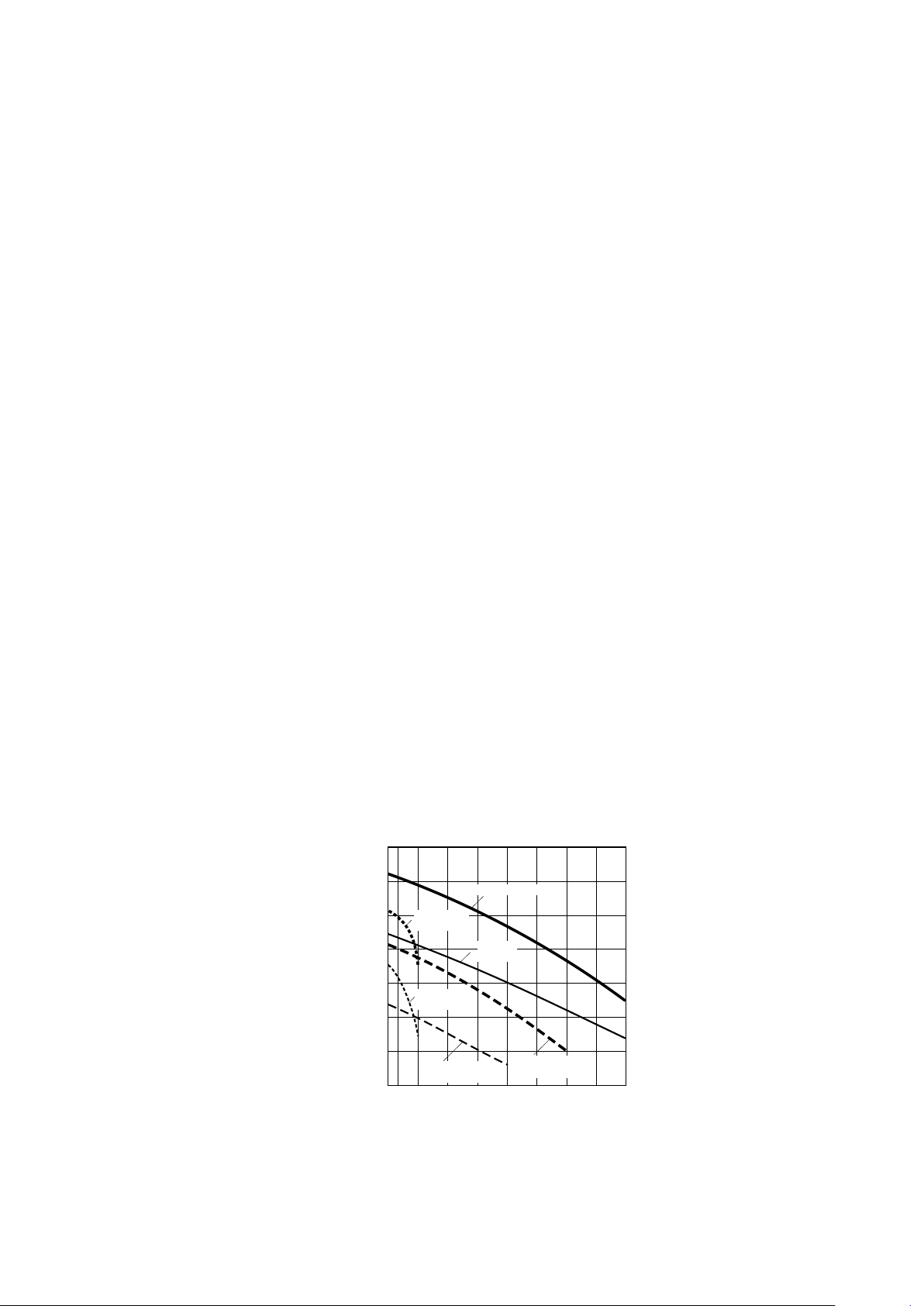
Figure 4 illustrates the predicted
OPB associated with the three
transceiver series specified in this
data sheet at the Beginning of
Life (BOL). These curves
represent the attenuation and
chromatic plus modal dispersion
losses associated with the 62.5/
125 µm and 50/125 µm fiber
cables only. The area under the
curves represents the remaining
OPB at any link length, which is
available for overcoming nonfiber cable related losses.
Hewlett-Packard LED technology
has produced 800 nm LED and
1300 nm LED devices with lower
aging characteristics than
normally associated with these
Figure 4. Optical Power Budget at BOL versus
Fiber Optic Cable Length.
OPTICAL POWER BUDGET (dB)
4.0
14
0
FIBER OPTIC CABLE LENGTH (km)
0.5 1.5 2.0 2.5
12
10
8
6
4
3.5
2
1.0 3.00.15
HFBR-5103, 62.5/125 µm
HFBR-5103,
50/125 µm
HFBR-5105,
62.5/125 µm
HFBR-5104,
62.5/125 µm
HFBR-5105,
50/125 µm
HFBR-5104,
50/125 µm
Page 6
131
TRANSCEIVER RELATIVE OPTICAL POWER BUDGET
AT CONSTANT BER (dB)
0 200
3.0
0
SIGNAL RATE (MBd)
25 75 100 125
2.5
2.0
1.5
1.0
175
0.5
50 150
CONDITIONS:
1. PRBS 2
7
-1
2. DATA SAMPLED AT CENTER OF DATA SYMBOL.
3. BER = 10
-6
4. TA = 25° C
5. V
CC
= 5 V
dc
6. INPUT OPTICAL RISE/FALL TIMES = 1.0/2.1 ns.
ment and the EIA/TIA-568-A
Commercial Building Telecommunications Cabling Standard per
SP-2840.
The HFBR-5104 series 800 nm
transceiver curve in Figure 4 was
generated based on extensive
empirical test data of typical 800
nm transmitter and receiver
performance. The curve includes
the effect of typical fiber attenuation, plus receiver sensitivity loss
due to chromatic and metal
dispersion losses through the
fiber.
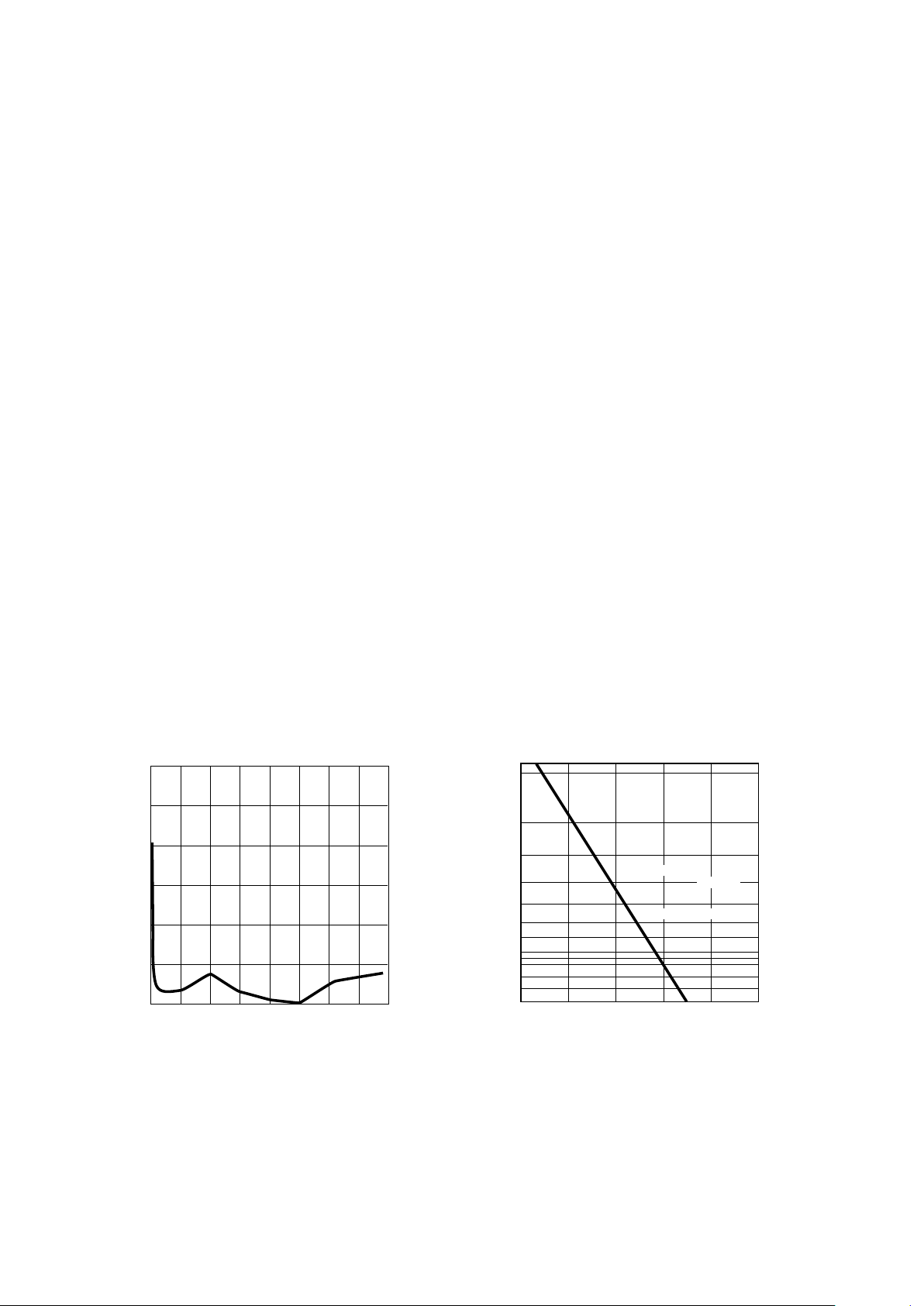
Transceiver Signaling
Operating Rate Range and
BER Performance
For purposes of definition, the
symbol (Baud) rate, also called
signaling rate, is the reciprocal of
the shortest symbol time. Data
rate (bits/sec) is the symbol rate
divided by the encoding factor
illustrates the typical trade-off
between link BER and the
receivers input optical power
level.
Transceiver Jitter
Performance
The Hewlett-Packard 1300 nm
transceivers are designed to
operate per the system jitter
allocations stated in Tables E1 of
Annexes E of the FDDI PMD and
LCF-PMD standards.
The HP 1300 nm transmitters will
tolerate the worst case input
electrical jitter allowed in these
tables without violating the worst
case output jitter requirements of
Sections 8.1 Active Output
Interface of the FDDI PMD and
LCF-PMD standards.
The HP 1300 nm receivers will
tolerate the worst case input
optical jitter allowed in Sections
8.2 Active Input Interface of the
used to encode the data (symbols/
bit).
When used in FDDI and ATM 100
Mbps applications the
performance of the 1300 nm
transceivers is guaranteed over
the signaling rate of 10 MBd to
125 MBd to the full conditions
listed in individual product
specification tables.
The transceivers may be used for
other applications at signaling
rates outside of the 10 MBd to
125 MBd range with some
penalty in the link optical power
budget primarily caused by a
reduction of receiver sensitivity.
Figure 5 gives an indication of
the typical performance of these
1300 nm products at different
rates.
These transceivers can also be
used for applications which
require different Bit Error Rate
(BER) performance. Figure 6
Figure 5. Transceiver Relative Optical Power Budget
at Constant BER vs. Signaling Rate.
Figure 6. Bit Error Rate vs. Relative Receiver Input
Optical Power.
BIT ERROR RATE
-6 4
1 x 10
-2
RELATIVE INPUT OPTICAL POWER – dB
-4 2-2
0
1 x 10
-4
1 x 10
-6
1 x 10
-8
2.5 x 10
-10
1 x 10
-11
HFBR-5103/-5104/-5105
CONDITIONS:
1. 125 MBd
2. PRBS 2
7
-1
3. CENTER OF SYMBOL SAMPLING.
4. T
A
= 25° C
5. V
CC
= 5 V
dc
6. INPUT OPTICAL RISE/FALL TIMES = 1.0/2.1 ns.
CENTER OF SYMBOL
1 x 10
-12
1 x 10
-7
1 x 10
-5
1 x 10
-3
SERIES
Page 7
132
FDDI PMD and LCF-PMD
standards without violating the
worst case output electrical jitter
allowed in the Tables E1 of the
Annexes E.
The jitter specifications stated in
the following 1300 nm
transceiver specification tables
are derived from the values in
Tables E1 of Annexes E. They
represent the worst case jitter
contribution that the transceivers
are allowed to make to the overall
system jitter without violating the
Annex E allocation example. In
practice the typical contribution
of the HP transceivers is well
below these maximum allowed
amounts.
Recommended Handling
Precautions
Hewlett-Packard recommends
that normal static precautions be
taken in the handling and
assembly of these transceivers to
prevent damage which may be
induced by electrostatic
discharge (ESD). The HFBR5100 series of transceivers meet
MIL-STD-883C Method 3015.4
Class 2 products.
Care should be used to avoid
shorting the receiver data or
signal detect outputs directly to
ground without proper current
limiting impedance.
Solder and Wash Process
Compatibility
The transceivers are delivered
with protective process plugs
inserted into the duplex SC or
duplex ST connector receptacle.
This process plug protects the
optical subassemblies during
wave solder and aqueous wash
processing and acts as a dust
cover during shipping.
These transceivers are compatible with either industry standard
wave or hand solder processes.
Shipping Container
The transceiver is packaged in a
shipping container designed to
protect it from mechanical and
ESD damage during shipment or
storage.
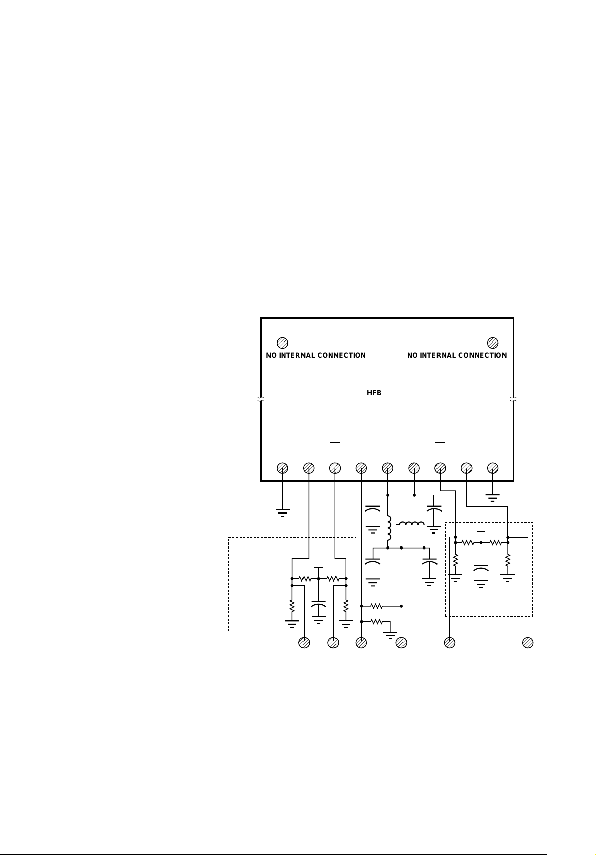
Board Layout - Decoupling
Circuit and Ground Planes
It is important to take care in the
layout of your circuit board to
achieve optimum performance
from these transceivers. Figure 7
provides a good example of a
schematic for a power supply
decoupling circuit that works well
with these parts. It is further
recommended that a contiguous
Figure 7. Recommended Decoupling and Termination Circuits
NO INTERNAL CONNECTION NO INTERNAL CONNECTION
HFBR-510X
TOP VIEW
V
EE
RD RD SD V
CCVCC
TD TD V
EE
123456789
C1 C2
L1 L2
R2 R3
R1 R4
C5
C3 C4
R9
R10
VCC FILTER
AT V
CC
PINS
TRANSCEIVER
R5 R7
R6 R8
C6
RD RD SD V
CC
TD TD
TERMINATION
AT PHY
DEVICE
INPUTS
NOTES:
THE SPLIT-LOAD TERMINATIONS FOR ECL SIGNALS NEED TO BE LOCATED AT THE INPUT
OF DEVICES RECEIVING THOSE ECL SIGNALS. RECOMMEND 4-LAYER PRINTED CIRCUIT
BOARD WITH 50 OHM MICROSTRIP SIGNAL PATHS BE USED.
TERMINATION
AT TRANSCEIVER
INPUTS
R1 = R4 = R6 = R8 = R10 = 130 OHMS.
R2 = R3 = R5 = R7 = R9 = 82 OHMS.
C1 = C2 = C3 = C5 = C6 = 0.1 µF.
C4 = 10 µF.
L1 = L2 = 1 µH COIL OR FERRITE INDUCTOR.
Rx Rx Tx Tx
V
CC
V
CC
Page 8

133
ground plane be provided in the
circuit board directly under the
transceiver to provide a low
inductance ground for signal
return current. This recommendation is in keeping with good high
frequency board layout practices.
Board Layout - Hole Pattern
The Hewlett-Packard transceiver
complies with the circuit board
“Common Transceiver Footprint”
hole pattern defined in the
original multisource announcement which defined the 1x9
package style. This drawing is
reproduced in Figure 8 with the
addition of ANSI Y14.5M
compliant dimensioning to be
used as a guide in the mechanical
layout of your circuit board.
Board Layout - Art Work
The Applications Engineering
group has developed Gerber file
artwork for a multilayer printed
circuit board layout incorporating
the recommendations above.
Contact your local HewlettPackard sales representative for
details.
Board Layout - Mechanical
For applications providing a
choice of either a duplex SC or a
duplex ST connector interface,
while utilizing the same pinout on
the printed circuit board, the ST
port needs to protrude from the
chassis panel a minimum of
9.53 mm for sufficient clearance
to install the ST connector.
Please refer to Figure 8a for a
mechanical layout detailing the
Figure 8. Recommended Board Layout Hole Pattern
recommended location of the
duplex SC and duplex ST transceiver packages in relation to the
chassis panel.
Regulatory Compliance
These transceiver products are
intended to enable commercial
system designers to develop
equipment that complies with the
various international regulations
governing certification of
Information Technology
Equipment. See the Regulatory
Compliance Table for details.
Additional information is
available from your HewlettPackard sales representative.
Electrostatic Discharge (ESD)
There are two design cases in
which immunity to ESD damage
is important.
(8X)
2.54
.100
20.32
.800
20.32
.800
1.9 ± 0.1
.075 ± .004
(2X)
ø
Ø0.000
MA
0.8 ± 0.1
.032 ± .004
(9X)
ø
Ø0.000
MA
–A–
TOP VIEW
Page 9

134
Figure 8a. Recommended Common Mechanical Layout for SC and ST 1x9 Connectored Transceivers.
25.4
42.0
24.8
9.53
(NOTE 1)
39.12
6.79
25.4
12.09
11.1
0.75
12.0
0.51
NOTE 1: MINIMUM DISTANCE FROM FRONT
OF CONNECTOR TO THE PANEL FACE.
Page 10

135
Regulatory Compliance Table
Feature Test Method Performance
Electrostatic Discharge MIL-STD-883C Meets Class 2 (2000 to 3999 Volts)
(ESD) to the Electrical Method 3015.4 Withstand up to 2200 V applied between
Pins electrical pins.
Electrostatic Discharge Variation of Typically withstand at least 25 kV without damage
(ESD) to the Duplex SC IEC 801-2 when the Duplex SC Connector Receptacle is
Receptacle contacted by a Human Body Model probe.
Electromagnetic FCC Class B Typically provide a 13 dB margin (with duplex SC
Interference (EMC) CENELEC CEN55022 package) or a 9 dB margin (with duplex ST
Class B (CISPR 22B) package) to the noted standard limits when tested
VCCI Class 2 at a certified test range with the transceiver
mounted to a circuit card without a chassis
enclosure.
Immunity Variation of IEC 801-3 Typically show no measurable effect from a
10 V/m field swept from 10 to 450 MHz
applied to the transceiver when mounted to a
circuit card without a chassis enclosure.
Figure 9. Transmitter Output Optical Spectral Width (FWHM) vs. Transmitter
Output Optical Center Wavelength and Rise/Fall Times.
The first case is during handling
of the transceiver prior to mounting it on the circuit board. It is
important to use normal ESD
handling precautions for ESD
sensitive devices. These
precautions include using
grounded wrist straps, work
benches, and floor mats in ESD
controlled areas.
The second case to consider is
static discharges to the exterior
of the equipment chassis containing the transceiver parts. To
the extent that the duplex SC
connector is exposed to the
outside of the equipment chassis
it may be subject to whatever
ESD system level test criteria that
the equipment is intended to
meet.
Electromagnetic Interference
(EMI)
Most equipment designs utilizing
these high speed transceivers
from Hewlett-Packard will be
required to meet the requirements of FCC in the United
States, CENELEC EN55022
(CISPR 22) in Europe and VCCI
in Japan.
1380
200
100
λC – TRANSMITTER OUTPUT OPTICAL
CENTER WAVELENGTH –nm
1200 1300 1320
180
160
140
120
13601340
∆λ – TRANSMITTER OUTPUT OPTICAL
SPECTRAL WIDTH (FWHM) –nm
t
r/f
– TRANSMITTER
OUTPUT OPTICAL
RISE/FALL TIMES – ns
1.5
2.0
3.0
3.5
2.5
3.0
3.5
HFBR-5103 FDDI TRANSMITTER TEST RESULTS
OF λ
C
, ∆λ AND t
r/f
ARE CORRELATED AND
COMPLY WITH THE ALLOWED SPECTRAL WIDTH
AS A FUNCTION OF CENTER WAVELENGTH FOR
VARIOUS RISE AND FALL TIMES.
Page 11

136
For additional information
regarding EMI, susceptibility,
ESD and conducted noise testing
procedures and results on the
1x9 Transceiver family, please
refer to Applications Note 1075,
Testing and Measuring Electromagnetic Compatibility
Performance of the HFBR510X/-520X Fiber Optic
Transceivers.
Transceiver Reliability
and Performance
Qualification Data
The 1x9 transceivers have passed
Hewlett-Packard reliability and
performance qualification testing
and are undergoing ongoing
quality monitoring. Details are
available from your HewlettPackard sales representative.
These transceivers are manufactured at the Hewlett-Packard
Singapore location which is an ISO
9002 certified facility.
Ordering Information
The HFBR-5103/-5103T and
HFBR-5105/-5105T 1300 nm
products and the HFBR-5104/
-5104T 800 nm products are available for production orders through
the Hewlett-Packard Component
Field Sales Offices and Authorized
Distributors world wide.
In all well-designed chassis, two
0.5" holes for ST connectors to
protrude through will provide
4.6 dB more shielding than one
1.2" duplex SC rectangular
cutout. Thus, in a well-designed
chassis, the duplex ST 1x9
transceiver emissions will be
identical to the duplex SC 1x9
transceiver emissions.
Immunity
Equipment utilizing these
transceivers will be subject to
radio-frequency electromagnetic
fields in some environments.
These transceivers have a high
immunity to such fields.
Figure 10. Output Optical Pulse Envelope.
40 ± 0.7
10.0
4.850
1.525
0.525
5.6
100% TIME
INTERVAL
± 0.725 ± 0.725
4.40
1.975
0.075
0.50
0.025
-0.025
0.0
-0.05
0.10
10.0
5.6
1.525
0.525
4.850
80 ± 500 ppm
4.40
1.975
0.075
0.90
1.025
1.25
TIME – ns
0% TIME
INTERVAL
1.00
0.975
RELATIVE AMPLITUDE
THE HFBR-5103 OUTPUT OPTICAL PULSE SHAPE SHALL FIT WITHIN THE BOUNDARIES OF THE
PULSE ENVELOPE FOR RISE AND FALL TIME MEASUREMENTS.
Page 12

137
Applications Support
Materials
Contact your local HewlettPackard Component Field Sales
Office for information on how to
obtain PCB layouts, test boards
and demo boards for the 1x9
transceivers.
Evaluation Kits
Hewlett-Packard has available
three evaluation kits for the 1x9
transceivers. The purpose of
these kits is to provide the necessary materials to evaluate the
performance of the HFBR-510X
family in a pre-existing 1x13 or
2x11 pinout system design
configuration or when connectored to various test equipment.
1. HFBR-0305 - ATM
Evaluation Kit
This kit consists of one HFBR5205, one 1x13 to 1x9 pinout
adapter card, and one three
meter duplex SC to duplex ST
connectored 62.5/125 µm fiber
optic cable.
2. HFBR-0303 - FDDI
Evaluation Kit
This kit consists of one HFBR5103, one 2x11 to 1x9 pinout
adapter card, one 1x13 to 1x9
pinout adapter card, and one
three meter duplex SC to MIC/
Receptacle connectored 62.5/
125 µm fiber optic cable.
3. HFBR-0319 Evaluation Test
Fixture Board
This test fixture converts +5 V
ECL 1x9 transceivers to –5 V
ECL BNC coax connections so
that direct connections to
industry standard fiber optic
test equipment can be
accomplished.
Accessory Duplex SC Connectored Cable Assemblies
Hewlett-Packard recommends for
optimal coupling the use of
flexible-body duplex SC connectored cable. Hewlett-Packard
offers two such compatible
Duplex SC connectored jumper
cable assemblies to assist you in
the evaluation of these transceiver products. These cables
may be purchased from HP with
the following part numbers.
1. HFBR-BKD001
A duplex cable 1 meter long
assembled with 62.5/125 µm
fiber and Duplex SC connector
plugs on both ends.
2. HFBR-BKD010
A duplex cable 10 meters long
assembled with 62.5/125 µm
fiber and Duplex SC connector
plugs on both ends.
Accessory Duplex ST
Connectored Cable
Assemblies
Hewlett-Packard recommends the
use of Duplex Push-Pull
connectored cable for the most
repeatable optical power coupling
performance.
Hewlett-Packard offers two such
compatible Duplex Push-Pull ST
connectored jumper cable
assemblies to assist you in your
evaluation of these products.
These cables may be purchased
from HP with the following part
numbers.
1. HFBR-XXX001
A duplex cable 1 meter long,
assembled with 62.5/125 µm
fiber and Duplex Push-Pull ST
connector plugs on both ends.
2. HFBR-XXX010
A duplex cable 10 meters long
assembled with 62.5/125 µm
fiber and Duplex Push-Pull ST
connector plugs on both ends.
Figure 11. Relative Input Optical Power vs. Eye
Sampling Time Position.
RELATIVE INPUT OPTICAL POWER (dB)
-4 4
0
EYE SAMPLING TIME POSITION (ns)
-3 -1 0 1
5
4
3
2
3
1
-2 2
2.5 x 10
-10
BER
1.0 x 10
-12
BER
CONDITIONS:
1.T
A
= 25° C
2. V
CC
= 5 Vdc
3. INPUT OPTICAL RISE/FALL TIMES = 1.0/2.1 ns.
4. INPUT OPTICAL POWER IS NORMALIZED TO
CENTER OF DATA SYMBOL.
5. NOTE 20 AND 21 APPLY.
HFBR-5103/-5104/-5105
SERIES
Page 13

138
Figure 12. Signal Detect Thresholds and Timing.
-31.0 dBm
-45.0 dBm
SIGNAL – DETECT (ON)
SIGNAL – DETECT (OFF)
AS – MAX
INPUT OPTICAL POWER
(> 1.5 dB STEP INCREASE)
INPUT OPTICAL POWER
(> 4.0 dB STEP DECREASE)
P
O
= MAX (PS OR -45.0 dBm)
(P
S
= INPUT POWER FOR BER < 102)
MIN (P
O
+ 4.0 dB OR -31.0 dBm)
P
A(PO
+ 1.5 dB < PA < -31.0 dBm)
OPTICAL POWER
TIME
SIGNAL
DETECT
OUTPUT
AS – MAX — MAXIMUM ACQUISITION TIME (SIGNAL).
AS – MAX IS THE MAXIMUM SIGNAL – DETECT ASSERTION TIME FOR THE STATION.
AS – MAX SHALL NOT EXCEED 100.0 µs. THE DEFAULT VALUE OF AS – MAX IS 100.0 µs.
ANS – MAX — MAXIMUM ACQUISITION TIME (NO SIGNAL).
ANS – MAX IS THE MAXIMUM SIGNAL – DETECT DEASSERTION TIME FOR THE STATION.
ANS – MAX SHALL NOT EXCEED 350 µs. THE DEFAULT VALUE OF AS – MAX IS 350 µs.
ANS – MAX
HFBR-5103, -5104, and -5105 Series
Absolute Maximum Ratings
Parameter Symbol Min. Typ. Max. Unit Reference
Storage Temperature T
S
-40 100 °C
Lead Soldering Temperature T
SOLD
260 °C
Lead Soldering Time t
SOLD
10 sec.
Supply Voltage V
CC
-0.5 7.0 V
Data Input Voltage V
I
-0.5 V
CC
V
Differential Input Voltage V
D
1.4 V Note 1
Output Current I
O
50 mA
Page 14

139
HFBR-5103, -5104 and -5105 Series
Recommended Operating Conditions
Parameter Symbol Min. Typ. Max. Unit Reference
Ambient Operating Temperature T
A
070°C
Supply Voltage V
CC
4.75 5.25 V
Data Input Voltage - Low VIL - V
CC
-1.810 -1.475 V
Data Input Voltage - High VIH - V
CC
-1.165 -0.880 V
Data and Signal Detect Output Load R
L
50 Ω Note 2
Transmitter Electrical Characteristics
(TA = 0°C to 70°C, VCC = 4.75 V to 5.25 V)
Parameter Symbol Min. Typ. Max. Unit Reference
Supply Current I
CC
145 185 mA Note 3
Power Dissipation P
DISS
0.76 0.97 W
Data Input Current - Low I
IL
-350 0 µA
Data Input Current - High I
IH
14 350 µA
Receiver Electrical Characteristics
(TA = 0°C to 70°C, VCC = 4.75 V to 5.25 V)
Parameter Symbol Min. Typ. Max. Unit Reference
Supply Current I
CC
82 145 mA Note 4
Power Dissipation P
DISS
0.3 0.5 W Note 5
Data Output Voltage - Low VOL - V
CC
-1.840 -1.620 V Note 6
Data Output Voltage - High VOH - V
CC
-1.045 -0.880 V Note 6
Data Output Rise Time t
r
0.35 2.2 ns Note 7
Data Output Fall Time t
f
0.35 2.2 ns Note 7
Signal Detect Output Voltage - Low VOL - V
CC
-1.840 -1.620 V Note 6
Signal Detect Output Voltage - High VOH - V
CC
-1.045 -0.880 V Note 6
Signal Detect Output Rise Time t
r
0.35 2.2 ns Note 7
Signal Detect Output Fall Time t
f
0.35 2.2 ns Note 7
Page 15

140
HFBR-5103/-5103T
Transmitter Optical Characteristics
(TA = 0°C to 70°C, VCC = 4.75 V to 5.25 V)
Parameter Symbol Min. Typ. Max. Unit Reference
Output Optical Power BOL P
O
-19 -16.8 -14 dBm avg. Note 11
62.5/125 µm, NA = 0.275 Fiber EOL -20
Output Optical Power BOL P
O
-22.5 -20.3 -14 dBm avg. Note 11
50/125 µm, NA = 0.20 Fiber EOL -23.5
Optical Extinction Ratio 0.001 0.03 % Note 13
-50 -35 dB
Output Optical Power at PO (“0”) -45 dBm avg. Note 14
Logic “0” State
Center Wavelength λ
C
1270 1308 1380 nm Note 15
Figure 9
Spectral Width - FWHM ∆λ 137 170 nm Note 15
Figure 9
Optical Rise Time t
r
0.6 1.0 3.0 ns Note 15, 16
Figure 9, 10
Optical Fall Time t
f
0.6 2.1 3.0 ns Note 15, 16
Figure 9, 10
Duty Cycle Distortion DCD 0.02 0.6 ns p-p Note 17
Contributed by the
Transmitter
Data Dependent Jitter DDJ 0.02 0.6 ns p-p Note 18
Cobntributed by the
Transmitter
Random Jitter Contributed RJ 0 0.69 ns p-p Note 19
by the Transmitter
Page 16

141
HFBR-5103/-5103T
Receiver Optical and Electrical Characteristics
(TA = 0°C to 70°C, VCC = 4.75 V to 5.25 V)
Parameter Symbol Min. Typ. Max. Unit Reference
Input Optical Power P
IN Min.
(W) -33.5 -31 dBm avg. Note 20
Minimum at Window Edge Figure 11
Input Optical Power P
IN Min.
(C) -34.5 -31.8 dBm avg. Note 21
Minimum at Eye Center Figure 11
Input Optical Power Maximum P
IN Max.
-14 -11.8 dBm avg. Note 20
Operating Wavelength λ 1270 1380 nm
Duty Cycle Distortion DCD 0.02 0.4 ns p-p Note 8
Contributed by the Receiver
Data Dependent Jitter DDJ 0.35 1.0 ns p-p Note 9
Contributed by the Receiver
Random Jitter Contributed RJ 1.0 2.14 ns p-p Note 10
by the Receiver
Signal Detect - Asserted P
A
PD + 1.5 dB -33 dBm avg. Note 22, 23
Figure 12
Signal Detect - Deasserted P
D
-45 dBm avg. Note 24, 25
Figure 12
Signal Detect - Hysteresis PA - P
D
1.5 2.4 dB Figure 12
Signal Detect Assert Time AS_Max 0 55 100 µs Note 22, 23
(off to on) Figure 12
Signal Detect Deassert Time ANS_Max 0 110 350 µs Note 24, 25
(on to off) Figure 12
Page 17

142
HFBR-5104/-5104T
Transmitter Optical Characteristics
(TA = 0°C to 70°C, VCC = 4.75 V to 5.25 V)
Parameter Symbol Min. Typ. Max. Unit Reference
Output Optical Power BOL P
O
-17 -12 dBm avg. Note 12
62.5/125 µm, NA = 0.275 Fiber EOL -20
Output Optical Power BOL P
O
-20.8 -12 dBm avg. Note 12
50/125 µm, NA = 0.20 Fiber EOL -23.8
Optical Extinction Ratio 0.01 % Note 13
-40 dB
Output Optical Power at PO (“0”) -45 dBm avg. Note 14
Logic “0” State
Center Wavelength λ
C
800 900 nm
Spectral Width - FWHM ∆λ 100 nm
Optical Rise Time t
r
4.5 ns Note 16a
Optical Fall Time t
f
4.5 ns Note 16a
Systematic Jitter Contributed SJ 1.7 ns p-p Note 26
by the Transmitter
Random Jitter Contributed RJ 0.69 ns p-p Note 27
by the Transmitter
Page 18

143
HFBR-5104/-5104T
Receiver Optical and Electrical Characteristics
(TA = 0°C to 70°C, VCC = 4.75 V to 5.25 V)
Parameter Symbol Min. Typ. Max. Unit Reference
Input Optical Power P
IN Min.
(W) -27.5 dBm avg. Note 20b
Minimum at Window Edge
Input Optical Power P
IN Min.
(C) -28 dBm avg. Note 21a
Minimum at Eye Center
Input Optical Power Maximum P
IN Max.
-12 dBm avg. Note 20b
Operating Wavelength λ 800 900 nm
Systematic Jitter Contributed SJ 1.2 ns p-p Note 26
by the Receiver
Random Jitter Contributed RJ 2.6 ns p-p Note 27
by the Receiver
Signal Detect - Asserted P
A
PD + 1.5 dB -29.5 dBm avg. Note 22
Signal Detect - Deasserted P
D
-45 dBm avg. Note 24
Signal Detect - Hysteresis PA - P
D
1.5 dB
Signal Detect Assert Time AS_Max 0 55 100 µs Note 22
(off to on)
Signal Detect Deassert Time ANS_Max 0 110 350 µs Note 24
(on to off)
Page 19

144
HFBR-5105/-5105T
Transmitter Optical Characteristics
(TA = 0°C to 70°C, VCC = 4.75 V to 5.25 V)
Parameter Symbol Min. Typ. Max. Unit Reference
Output Optical Power BOL P
O
-21 -14 dBm avg. Note 11
62.5/125 µm, NA = 0.275 Fiber EOL -22
Output Optical Power BOL P
O
-24.5 -14 dBm avg. Note 11
50/125 µm, NA = 0.20 Fiber EOL -25.5
Optical Extinction Ratio 0.001 0.03 % Note 13
-50 -35 dB
Output Optical Power at PO (“0”) -45 dBm avg. Note 14
Logic “0” State
Center Wavelength λ
C
1270 1308 1380 nm
Spectral Width - FWHM ∆λ 137 250 nm
Optical Rise Time t
r
4 ns Note 16a
Optical Fall Time t
f
4 ns Note 16a
Duty Cycle Distortion DCD 0.02 0.6 ns p-p Note 17
Contributed by the Transmitter
Data Dependent Jitter DDJ 0.02 0.6 ns p-p Note 18
Contributed by the Transmitter
Random Jitter Contributed RJ 0 0.69 ns p-p Note 19
by the Transmitter
Page 20

145
HFBR-5105/-5105T
Receiver Optical and Electrical Characteristics
(TA = 0°C to 70°C, VCC = 4.75 V to 5.25 V)
Parameter Symbol Min. Typ. Max. Unit Reference
Input Optical Power P
IN Min.
(W) -29 dBm avg. Note 20a
Minimum at Window Edge Figure 11
Input Optical Power P
IN Min.
(C) -29.8 dBm avg. Note 21a
Minimum at Eye Center Figure 11
Input Optical Power Maximum P
IN Max.
-14 dBm avg. Note 20a
Operating Wavelength λ 1270 1380 nm
Duty Cycle Distortion DCD 0.02 0.4 ns p-p Note 8
Contributed by the Receiver
Data Dependent Jitter DDJ 0.35 1.0 ns p-p Note 9
Contributed by the Receiver
Random Jitter Contributed RJ 1.0 2.9 ns p-p Note 10
by the Receiver
Signal Detect - Asserted P
A
PD + 1.5 dB -31 dBm avg. Note 22,
23a
Signal Detect - Deasserted P
D
-45 dBm avg. Note 24,
25a
Signal Detect - Hysteresis PA - P
D
1.5 2.4 dB
Signal Detect Assert Time AS_Max 0 55 100 µs Note 22,
(off to on) 25a
Signqal Detect Deassert Time ANS_MAX 0 110 350 µs Note 24,
(on to off) 25a
Notes:
1. This is the maximum voltage that
can be applied across the Differential Transmitter Data Inputs to
prevent damage to the input ESD
protection circuit.
2. The outputs are terminated with
50 Ω connected to VCC -2 V.
3. The power supply current needed to
operate the transmitter is provided
to differential ECL circuitry. This
circuitry maintains a nearly constant current flow from the power
supply. Constant current operation
helps to prevent unwanted electrical
noise from being generated and
conducted or emitted to neighboring
circuitry.
4. This value is measured with the outputs terminated into 50 Ω connected
to VCC - 2 V and an Input Optical
Power level of -14 dBm average.
5. The power dissipation value is the
power dissipated in the receiver
itself. Power dissipation is calculated as the sum of the products of
supply voltage and currents, minus
the sum of the products of the
output voltages and currents.
6. This value are measured with
respect to VCC with the output
terminated into 50 Ω connected to
VCC - 2 V.
7. The output rise and fall times are
measured between 20% and 80%
levels with the output connected to
VCC -2 V through 50 Ω.
8. Duty Cycle Distortion contributed
by the receiver is measured at the
50% threshold using an IDLE Line
State, 125 MBd (62.5 MHz squarewave), input signal. The input
optical power level is -20 dBm
average. See Application
Information - Transmitter Jitter
Section for further information.
9. Data Dependent Jitter contributed by
the receiver is specified with the
FDDI DDJ test pattern described in
the FDDI PMD Annex A.5. The
input optical power level is -20 dBm
average. See Application Information - Transmitter Jitter Section for
further information.
10. Random Jitter contributed by the
receiver is specified with an IDLE
Line State, 125 MBd (62.5 MHz
square-wave), input signal. The
input optical power level is at maximum “P
IN Min.
(W)”. See Application
Information - Transmitter Jitter
Section for further information.
Page 21

146
11. These optical power values are
measured with the following
conditions:
• The Beginning of Life (BOL) to
the End of Life (EOL) optical
power degradation is typically 1.5
dB per the industry convention for
long wavelength LEDs. The actual
degradation observed in HewlettPackard’s 1300 nm LED products
is < 1 dB, as specified in this data
sheet.
• Over the specified operating
voltage and temperature ranges.
• With HALT Line State, (12.5 MHz
square-wave), input signal.
• At the end of one meter of noted
optical fiber with cladding modes
removed.
The average power value can be
converted to a peak power value by
adding 3 dB. Higher output optical
power transmitters are available on
special request.
12. The same comments of note 11
apply except that industry convention for short wavelength LED (800
nm) BOL to EOL aging is 3 dB. This
value for Output Optical Power will
provide a minimum of a 6 dB optical
power budget at the EOL, which
will provide at least 500 meter link
lengths with margin left over for
overcoming normal passive losses,
such as in line connectors, in the
cable plant. The actual degradation
observed in normal commercial
environments will be considerably
less than this amount with HewlettPackard’s 800 nm LED products.
Please consult with your local HP
sales representative for further
details.
13. The Extinction Ratio is a measure of
the modulation depth of the optical
signal. The data “0” output optical
power is compared to the data “1”
peak output optical power and
expressed as a percentage. With the
transmitter driven by a HALT Line
State (12.5 MHz square-wave)
signal, the average optical power is
measured. The data “1” peak power
is then calculated by adding 3 dB to
the measured average optical power.
The data “0” output optical power is
found by measuring the optical
power when the transmitter is
driven by a logic “0” input. The
extinction ratio is the ratio of the
optical power at the “0” level
compared to the optical power at the
“1” level expressed as a percentage
or in decibels.
14. The transmitter provides
compliance with the need for
Transmit_Disable commands from
the FDDI SMT layer by providing
an Output Optical Power level of
< -45 dBm average in response to a
logic “0” input. This specification
applies to either 62.5/125 µm or
50/125 µm fiber cables.
15. This parameter complies with the
FDDI PMD requirements for the
tradeoffs between center wavelength, spectral width, and rise/fall
times shown in Figure 9.
16. This parameter complies with the
optical pulse envelope from the
FDDI PMD shown in Figure 10. The
optical rise and fall times are
measured from 10% to 90% when
the transmitter is driven by the
FDDI HALT Line State (12.5 MHz
square-wave) input signal.
16a. The optical rise and fall times are
measured from 10% to 90% when
the transmitter is driven by the
FDDI HALT Line State (12.5 MHz
square-wave) input signal.
17. Duty Cycle Distortion contributed
by the transmitter is measured at a
50% threshold using an IDLE Line
State, 125 MBd (62.5 MHz squarewave), input signal. See Application
Information - Transceiver Jitter
Performance Section of this data
sheet for further details.
18. Data Dependent Jitter contributed
by the transmitter is specified with
the FDDI test pattern described in
FDDI PMD Annex A.5. See Application Information - Transceiver Jitter
Performance Section of this data
sheet for further details.
19. Random Jitter contributed by the
transmitter is specified with an
IDLE Line State, 125 MBd (62.5
MHz square-wave), input signal.
See Application Information Transceiver Jitter Performance
Section of this data sheet for further
details.
20. This specification is intended to
indicate the performance of the
receiver section of the transceiver
when Input Optical Power signal
characteristics are present per the
following definitions. The Input
Optical Power dynamic range from
the minimum level (with a window
time-width) to the maximum level is
the range over which the receiver is
guaranteed to provide output data
with a Bit Error Ratio (BER) better
than or equal to 2.5 x 10
-10
.
• At the Beginning of Life (BOL)
• Over the specified operating
temperature and voltage ranges
• Input symbol pattern is the FDDI
test pattern defined in FDDI PMD
Annex A.5 with 4B/5B NRZI
encoded data that contains a duty
cycle base-line wander effect of
50 kHz. This sequence causes a
near worst case condition for
inter-symbol interference.
• Receiver data window time-width
is 2.13 ns or greater and centered
at mid-symbol. This worst case
window time-width is the
minimum allowed eye-opening
presented to the FDDI PHY
PM._Data indication input (PHY
input) per the example in FDDI
PMD Annex E. This minimum
window time-width of 2.13 ns is
based upon the worst case FDDI
PMD Active Input Interface
optical conditions for peak-to-peak
DCD (1.0 ns), DDJ (1.2 ns) and RJ
(0.76 ns) presented to the
receiver.
To test a receiver with the worst
case FDDI PMD Active Input jitter
condition requires exacting control
over DCD, DDJ and RJ jitter components that is difficult to implement
with production test equipment. The
receiver can be equivalently tested
to the worst case FDDI PMD input
jitter conditions and meet the
minimum output data window timewidth of 2.13 ns. This is accomplished by using a nearly ideal input
optical signal (no DCD, insignificant
DDJ and RJ) and measuring for a
wider window time-width of 4.6 ns.
This is possible due to the cumulative effect of jitter components
through their superposition (DCD
and DDJ are directly additive and
RJ components are rms additive).
Specifically, when a nearly ideal
input optical test signal is used and
the maximum receiver peak-to-peak
jitter contributions of DCD (0.4 ns),
DDJ (1.0 ns), and RJ (2.14 ns) exist,
the minimum window time-width
becomes 8.0 ns -0.4 ns - 1.0 ns - 2.14
ns = 4.46 ns, or conservatively
4.6 ns. This wider window time-
width of 4.6 ns guarantees the FDDI
PMD Annex E minimum window
time-width of 2.13 ns under worst
case input jitter conditions to the
Hewlett-Packard receiver.
• Transmitter operating with an
Page 22

147
IDLE Line State pattern, 125
MBd (62.5 MHz square-wave),
input signal to simulate any
cross-talk present between the
transmitter and receiver sections
of the transceiver.
20a. All the conditions of Note 20 apply
except that the BER requirement is
tightened to 1 x 10
-12
and the
minimum window time-width test
condition is narrowed from 4.6 ns to
3.7 ns to reflect the lesser amount of
worst case input optical jitter as a
result of shorter optical cable
lengths and lower BER which are
both attributes of the FDDI LCFPMD.
20b. All the conditions of Note 20 apply
except that the BER requirement is
tightened to 1 x 10
-12
and the
minimum window time-width test
condition is adjusted to 4.2 ns to
reflect the HFBR-5104 transmitter
contributed jitter values per the
specification table.
21. All conditions of Note 20 apply
except that the measurement is
made at the center of the symbol
with no window time-width.
21a. All the conditions of Note 21 apply
accept that the BER requirement is
tightened to 1 x 10
-12
.
22. This value is measured during the
transition from low to high levels of
input optical power.
23. The Signal Detect output shall be
asserted within 100 µs after a step
increase of the Input Optical Power.
The step will be from a low Input
Optical Power, ≤ -45 dBm, into the
range between greater than PA, and
-14 dBm. The BER of the receiver
output will be 10-2 or better during
the time, LS_Max (15 µs) after
Signal Detect has been asserted. See
Figure 12 for more information.
23a. The Signal Detect output shall be
asserted within 100 µs after a step
increase of the Input Optical Power.
The step will be from a low Input
Optical Power, ≤ -45 dBm, into the
range -27 dBm ± 2 dB. The BER of
the receiver output will be 10-2 or
better during the time, LS_Max
(15 µs) after Signal Detect has been
asserted.
24. This value is measured during the
transition from high to low levels of
input optical power. The maximum
value will occur when the input
optical power is either -45 dBm
average or when the input optical
power yields a BER of 10-2 or better,
whichever power is higher.
25. Signal detect output shall be deasserted within 350 µs after a step
decrease in the Input Optical Power
from a level which is the lower of;
-31 dBm or PD + 4 dB (PD is the
power level at which signal detect
was deasserted), to a power level of
-45 dBm or less. This step decrease
will have occurred in less than 8 ns.
The receiver output will have a BER
of 10-2 or better for a period of 12 µs
or until signal detect is deasserted.
The input data stream is the Quiet
Line State. Also, signal detect will
be deasserted within a maximum of
350 µs after the BER of the receiver
output degrades above 10-2 for an
input optical data stream that
decays with a negative ramp function instead of a step function. See
Figure 12 for more information.
25a. Signal detect output shall be de-
asserted within 350 µs after a step
decrease in the Input Optical Power.
The step decrease signal shall have
an on level of -27 dBm ± 2 dB and
an off power level of -45 dBm or less.
This step decrease will have
occurred in less than 8 ns. The
receiver outputs within 12 µs after
the step decrease in the optical
power will not reproduce with an
accuracy greater than 90% any
spurious signals (e.g. symbols from
adjacent physical link components
or power supply ripple). The input
data stream is the Quiet Line State.
Signal detect will also be deasserted
within a maximum of 350 µs after
the BER of the receiver output
degrades above 10-2 for an input
optical data stream that decays with
a negative ramp function with a
response time > 8 ns.
26. Systematic Jitter (SJ) contributed
by the 800 nm transmitter is a combination of Duty Cycle Distortion
(DCD) and Data Dependent Jitter
(DDJ).
27. Random Jitter contributed by the
800 nm transmitter is specified with
an IDLE Line State, 125 MBd (62.5
MHz square-wave), input signal.
 Loading...