

Page 1
Single Chip 10BASE-FL
Transceiver
Technical Data
HFBR-4663
General Description
The HFBR-4663 Single Chip
10BASE-FL Transceiver is a
highly integrated circuit for IEEE
802.3 10Base-FL transceivers.
This product, when used with
HP’s fiber-optic transmitters and
receivers (HFBR-14X4 and
HFBR-2416), ensures
compliance to the 10Base-FL
Standard with a minimum
number of external components
and board space.
The HFBR-4663 offers a standard
IEEE 802.3 AU interface that
allows it to be directly connected
to industry standard manchester
encoder/decoder chips or an AUI
connector. The fiber-optic LED
driver offers a current drive
output that directly drives the
HFBR-14X4 transmitter. The data
quantizer section of the HFBR4663 is directly compatible with
the output of the HFBR-24X6
fiber-optic receiver and is capable
of accepting input signals as low
as 2 mVp-p with a 55 dB dynamic
range.
The transmitter automatically
inserts 1 MHz signal during idle
time and removes this signal on
reception. Low light is continuously monitored for both activity
as well as power level. Five LED
status indicators monitor error
conditions as well as transmissions, receptions, and collisions.
Features
• Single Chip Solution for
10BASE-FL Internal or
External Medium
Attachment Units (MAUs)
• Specifically Designed for Use
with HFBR-14X4 and HFBR24X6 Fiber-optic
Transmitters and Receivers
• Incorporates an AU Interface
• Highly Stable Data Quantizer
with 55 dB Input Dynamic
Range
• Input Sensitivity as Low
as 2 mV
P-P
• Current Driven Fiber Optic
LED Driver for Accurate
Launch Power
• Single +5 Volt Supply
• No Crystal or Clock
Required
• Five Network Status LED
Outputs
• Available in 28 Pin PCC
Package
• Semi-Standard Option
Available
CAUTION: The small junction sizes inherent to the design of this component increase the component's susceptibility to damage from electrostatic discharge (ESD). It is advised that normal static precautions be taken in
handling and assembly of this component to prevent damage and/or degradation which may be induced by
ESD.
5965-8597E (5/97)
77
Page 2
Block Diagram
SQEN/JABD
VCCTx
(+5 V)
+5 V
RTSET
GND
AV
CC
Tx+
Tx-
COL+
COL-
Rx+
Rx-
AUI
RECEIVER
Tx
SQUELCH
AUI
DRIVER
AUI
DRIVER
1 MHz IDLE
SIGNAL
SQE
10 MHz GATED
OSCILLATOR
LOOPBACK
MUX
Tx
Rx
FIBER OPTIC
DRIVER
JABBER
RECEIVE SQUELCH
CMP
LED
LINK DETECT
AMP
LED
DRIVERS
BIAS
V
REF
TxOUT
XMT
RCV
CLSN
JAB
LMON
VIN+
VIN-
V
DC
V
REF
V
THADJ
78
GND
V
CC
(+5 V)
+5 V
RRSET
LBDIS AGND
C
TIMER
Page 3
Pin Connection
28 – PIN PCC Q – 28
SQEN/JABD
Rx+
Rx-
LBDIS
V
CC
Tx+
Tx-
TIMER
C
COL-
COL+
CLSN
JAB
4321282726
5
6
7
8
9
10
11
12 13 14 15 16 17 18
XMT
RCV
RRSET
TOP VIEW
LMON
RTSET
AVCCV
Tx
CC
V
IN+
25
24
23
22
21
20
19
TxOUT
V
IN-
AGND
V
THADJ
V
REF
V
DC
GND
GND
Pin Description
Pin Name Function
1 CLSN Indicates that a collision is taking place. Active low LED driver, open collector.
Event is extended with internal timer for visibility.
2 COL+ Gated 10 MHz oscillation used to indicate a collision, SQE test, or jabber.
3 COL- Balanced differential line driver outputs that meet AUI specifications.
4C
TIMER
5 SQEN/JABD SQE Test Enable, jabber Disable. When tied low, SQE test is disabled, when tied
6 Rx+ Manchester encoded receive data output to the local device. Balanced
7 Rx- differential line driver outputs that meet AUI specifications.
8 LBDIS Loopback Disable. When this pin is tied to VCC, the AUI transmit pair data is not
9V
CC
10 Tx+ Balanced differential line receiver inputs that meet AUI specifications. These
11 Tx- inputs may be transformer or capacitively coupled. The Tx input pins are
12 RTSET Sets the current driven output of the transmitter.
13 RRSET A 1% 61.9 kΩ resistor tied from this pin to VCC sets the biasing currents for
14 LMON Link Monitor “Low Light” LED status output. This pin is pulled low when the
A capacitor from this pin to VCC determines the Link Monitor response time.
high SQE test is enabled. When tied to 2.0 V both SQE test and jabber are
disabled.
looped back to the AUI receive pair, and collision is disabled. When this pin is
tied to GND (normal operation) or left floating, the AUI transmit pair data is
looped back to the AUI receiver pair, except during collision.
+5 V power input.
internally DC biased for AC coupling.
internal nodes.
voltage on the VIN+, VIN- inputs exceed the minimum threshold set by the V
pin, and there are transitions on VIN+, VIN- indicating an idle signal or active
data. If either the voltage on the VIN+, VIN- inputs fall below the minimum
threshold or transitions cease on VIN+, VIN-, LMON will go high. Active low LED
driver, open collector.
THADJ
79
Page 4
Pin Description (cont.)
Pin Name Function
1 5 XMT Indicates that transmission is taking place. Active low LED driver, open
collector. Event is extended with internal timer for visibility.
1 6 RCV Indicates that the transceiver is receiving a frame from the optical input. Active
low LED driver, open collector. Event is extended with internal timer for
visibility.
17 VCCTx +5 V supply for fiber optic LED driver.
18 TxOUT Fiber optic LED driver output.
19 GND Ground Reference.
20 GND Ground Reference.
21 V
22 V
23 V
DC
REF
THADJ
24 AGND Analog Filtered Ground.
25 VIN- This input pin should be capacitively coupled to the input source or to filtered
An external capacitor on this pin integrates an error signal which nulls the
offset of the input amplifier. If the DC feedback loop is not being used, this pin
should be connected to V
REF
.
A 2.5 V reference with respect to GND.
This input pin sets the link monitor threshold.
AVCC. (The input resistance is approximately 1.3 kΩ.)
26 VIN+ This input pin should be capacitively coupled to the input source or to filtered
AVCC. (The input resistance is approximately 1.3 kΩ.)
27 AV
CC
Analog Filtered +5 V.
28 JAB Jabber network status LED. When in the jabber state, this pin will be low and
the transmitter will be disabled. In the jabber “OK” state this pin will be high.
Active low LED, open collector.
Absolute Maximum Ratings
[1]
Parameter Symbol Min. Max. Units
Storage Temperature T
Operating Temperature T
S
A
-65 +150 C
070C
Lead Soldering Cycle 260 C
Temperature
Lead Soldering Cycle Time 10 sec
Power Supply Voltage Range V
CC
-0.3 6.0 V
Input Voltage Range Digital Inputs (SQEN, LBDIS) -0.3 6.0 V
Tx+, Tx-, VIN+, VIN- -0.3 6.0 V
Input Current RRSET, RTSET, JAB, CLSN, 60 mA
XMT, RCV, LMON
Output Current TxOUT 70 mA
80
Page 5
Operating Conditions
Parameter Min. Typ. Max. Units
Supply Voltage (VCC) 4.75 5.0 5.25 V
LED on Current 10 mA
RRSET 61.9 k ± 1% Ω
RTSET 140 ± 1% Ω
Electrical Characteristics
[4]
[2,3]
220 mA
0.8 V
-200 10 +200 µA
567mV
Unless otherwise specified, TA = 0°C to 70°C, VCC = VCCTx = 5 V ± 5%
Parameter Condition Min. Typ. Max. Units
Power Supply Current ICC:V
= 5 V, RTSET = 140 Ω
CC
While Transmitting
LED Drivers: V
CC
Transmit Peak Output Current
[6]
IOL = 10 mA
RTSET = 140 Ω 47 52 57 mA
[5]
Transmit Squelch Voltage Level -300 -250 -200 mV
(Tx+, Tx-)
Differential Output Voltage ± 550 ± 1200 mV
(Rx± , COL± )
Common Mode Output Voltage 4.0 V
(Rx± , COL± )
Differential Output Voltage ± 40 mV
Imbalance (Rx± , COL± )
SQE/JABD SQE Test Disable 0.3 V
Both Disabled 1.5 VCC - 2 V
Both Enabled VCC - 0.5 V
LBDIS Threshold Disabled VCC - 0.1 V
Enabled 1 V
Common Mode Voltage (Tx+, Tx-) 3.5 V
Common Mode Voltage (VIN+, VIN-) 1.65 V
Reference Voltage 2.35 2.45 2.55 V
V
Output Source Current 5 mA
REF
Amplifier Gain 100 V/V
Input Signal Range 2 1600 mV
External Voltage at V
Set V
TH
Input Offset VDC = V
to 0.5 2.7 V
THADJ
(DC loop active) 3 mV
REF
Input Referred Noise 50 MHz BW 25 µV
Input Resistance VIN+, VIN- 0.8 1.3 2.0 kΩ
Input Bias Current of V
Input Threshold Voltage V
THADJ
THADJ
= V
REF
[7]
Hysteresis 20 %
P-P
P-P
81
Page 6

AC Electrical Characteristics
Symbol Parameter Min. Typ. Max. Units
Transmit
t
TXNPW
t
TXFPW
t
TXLP
t
TXODY
t
TXIDF
t
TXDC
t
TXSDY
t
TXJ
Receive
t
RXSFT
t
RXODY
t
RXFX
t
RXSDY
t
RXJ
t
AR
tAFDifferential Output Fall Time 20% to 80% (Rx± , COL± )4ns
Collision
t
CPSQE
t
SQEXR
t
CLF
t
CLPDC
t
SQEDY
t
SQETD
Jabber and LED Timing
t
JAD
`t
JRT
t
JSQE
t
LED
t
LLPH
t
LLCL
Transmit Turn-On Pulse Width 20 ns
Transmit Turn-Off Pulse Width from Data to Idle 400 2100 ns
Transmit Loopback Start-up Delay 500 ns
Transmit Turn-On Delay 100 ns
Transmit Idle Frequency 0.85 1.25 MHz
Transmit Idle Duty Cycle 45 55 %
Transmit Steady State Propagation delay 15 50 ns
Transmit Jitter into 31 Ω Load ± 1.5 ns
Receive Squelch Frequency Threshold 2.51 4.5 MHz
Receive Turn-On Delay 270 ns
Last Bit Received to Slow Decay Output 230 300 ns
Receive Steady State Propagation Delay 15 50 ns
Receive Jitter ± 1.5 ns
Differential Output Rise Time 20% to 80% (Rx± , COL± )4ns
Collision Present to SQE Assert 0 350 ns
Time for SQE to Deactivate After Collision 0 700 ns
Collision Frequency 8.5 11.5 MHz
Collision Pulse Duty Cycle 40 50 60 %
SQE Test Delay (Tx Inactive to SQE) 0.6 1.6 µs
SQE Test Duration 0.5 1.0 1.5 µs
Jabber Activation Delay 20 70 150 ms
Jabber Reset Unjab Time 250 450 750 ms
Delay from Outputs Disabled to Collision Oscillator On 100 ns
RCV, CLSN, XMT On Time 8 16 32 ms
Low Light Present to LMON High 3 5 10 µs
Low Light Present to LMON Low 250 750 ms
Notes:
1. Absolute maximum ratings are limits beyond which the life of the integrated circuit may be impaired. All voltages unless otherwise
specified are measured with respect to ground.
2. Limits are guaranteed by 100% testing, sampling, or correlation with worst-case test conditions.
3. Low Duty Cycle pulse testing is performed at TA.
4. This does not include the current from the AUI pull-down resistors, or LED status otuputs.
5. LED drivers can sink up to 20 mA, but VOL will be higher.
6. Does not include pre-bias current for fiber optic LED which would typically be 3 mA.
7. Threshold for switching from Link Fail ot Link Pass (Low Light).
82
Page 7

83
C11 MUST BE
PHYSICALLY CLOSE
TO U3
HFBR-14X4
+VRF
–VRF
C11
0.1
1
1
1
1
8
U3
54
8
6
37
1
2
6
7
3
R1 10 Ω
HFBR-24X6
5
4
R14
1K Ω
C4 0.047
C5 0.1
C3
0.01
C1
0.1
U1
C2
0.01
2
R12
0
R13
00
–VRF
C12
0.1
18
17
21
26
25
22
23
R8
100 Ω ±1%
Figure 1. HFBR-4663 Schematic Diagram.
R15
1.5 K Ω
D2
HLMP-1790D3HLMP-1790D4HLMP-1700D5HLMP-1719D6HLMP-1790D7HLMP-1700
14 28
MON
CC
8
4
TXOUT
TXV
LBDIS
C TIMER
VDC
VIN+
VIN–
VREF
VTHADJ
R16
1.5 K Ω
1
JAB
CLSN
U5
HFBR-4663
16
RCV
∞
GND
–VRF
+VRF
RRSET
RTSET
20
12 13
27 24
R9
61.9 K Ω
±1%
15
XMT
GND
19 9
R17
1.5 K Ω
COL–
COL+
TX–
TX+
RX–
RX+
SQE
CC
V
R18
1.5 K Ω
R2
360 Ω
3
R3
360 Ω
2
R4 39 Ω
11
R5
39 Ω
10
R6 360 Ω
7
R7
360 Ω
6
5
C10
0.1
–VRF
+VRF
C6
22
NOTES:
1. ALL RESISTORS ±5% UNLESS OTHERWISE SHOWN.
2. ALL CAPACITORS ±10% UNLESS OTHERWISE SHOWN.
3. THE HFBR-4663 DATA SHEET (PUBLICATION #5091-7391E 4/93)
CONTAINS ERRORS THAT HAVE SUBSEQUENTLY BEEN
CORRECTED IN THIS SCHEMATIC.
4. ALL CAPACITORS ARE IN µF.
R19
1.5 K Ω
C13
0.1
11
1
1
R10
3 K Ω
10
+
6
1
2
4
5
7
8
VIN
U4
LM2574
VGND
5
1.5 K Ω
16
PE65728
15
13
12
10
9
U2
ON
4
R20
R11
5 K Ω
OUT
SGND
FB
1N5817
V
CC
U12
1
9
2
10
3
11
4
12
5
13
6
(+12 VOLTS
7
8
FROM AUI
CONNECTOR)
DB 15
C9
0.1
V
CC
+VRF
–VRF
14
15
3
12
D1
L1
470 µH
+
470
±20%
L2
4.7 µH
C7
L3
4.7 µH
+
C8
10
±20%
Page 8

System Description
Figure 1 shows a schematic
diagram of the HFBR-4663 in an
internal or external 10BASE-FL
MAU. On one side of the
transceiver is the AU interface
and the other is the fiber optic
interface. The AU interface is AC
coupled when used in an external
transceiver or an internal
transceiver. The AU interface for
an external transceiver includes
isolation transformers, some
biasing resistors, and a voltage
regulator for power.
The fiber optic side of the
transceiver requires an external
fiber optic transmitter and fiber
optic receiver. The transmitter
uses a current driven output that
directly drives the fiber optic
transmitter. The receive side of
the transceiver accepts the data
after passing through a fiber optic
receiver, which consists of a
module containing a pin diode
and a transimpedance amplifier.
AU Interface
The AU interface consists of 3
pairs of signals, DO, CI and DI as
shown in Figure 1. The DO pair
contains transmit data from the
DTE which is received by the
transceiver and sent out onto the
fiber optic cable. The DI pair
contains valid data that has been
either received from the fiber
optic cable or looped back from
the DO and output through the DI
pair to the DTE. The CI pair
indicates whether a collision has
occurred. It is an output that
oscillates at 10 MHz if a collision,
jabber or SQE Test has taken
place, otherwise it remains idle.
When the transceiver is external,
these three pairs are AC coupled
through isolation transformers,
while an internal transceiver may
be capacitively coupled. Tx+, Txis internally DC biased (shifted up
in voltage) for the proper
common mode input voltage.
The two 39 Ω 1% resistors (or
one 78 Ω 1% resistor) tied to he
Tx+ and Tx- pins will provide the
proper termination. The CI and DI
pair, which are output from the
transceiver to the AUI cable,
require 360 Ω pull down resistors
when terminated with a 78 Ω
load. However on a DTE card, CI
and DI do not need 78 Ω
terminating resistors. This also
means that the pull down resistors
on CI and DI can be 1 kΩ or
greater depending upon the
particular Manchester encoder/
decoder chip used. Using higher
value pull down resistors as in a
DTE card will save power.
The AUI drivers are capable of
driving the full 50 meters of cable
length and have a rise and fall
time of typically 4 ns. In the idle
state, the outputs go to the same
voltage to prevent DC standing
current in the isolation
transformers.
Transmission
The transmit function consists of
detecting the presence of data
from the AUI DO input (Tx+, Tx-)
and driving that data onto the
fiber optic LED transmitter. A
positive signal on the Tx+ lead
relative to the Tx- lead of the DO
circuit will result in no current,
hence the fiber optic LED is in a
low light condition. When Tx+ is
more negative than Tx-, the
HFBR-4663 will sink current into
the chip and the fiber optic LED
will emit light.
Before data will be transmitted
onto the fiber optic cable from
the AU interface, it must exceed
the squelch requirements for the
DO pair. The Tx squelch circuit
serves the function of preventing
any noise from being transmitted
onto the fiber. This circuit rejects
signals with pulse widths less than
typically 20 ns (negative going),
or with levels less than -250 mV.
Once Tx squelch circuit has
unsquelched, it looks for the start
of idle signal to turn on the
squelch circuit again. The
transmitter turns on the squelch
again when it receives an input
signal at Tx+, Tx- that is more
positive than -250 mV for more
than approximately 180 ns.
At the start of a packet transmission, no more than 2 bits are
received from the DO circuit and
not transmitted onto the fiber
optic cable. The difference
between start-up delays (bit loss
plus steady-state propagation
delay) for any two packets that
are separated by 9.6 µs or less
will not exceed 200 ns.
Fiber Optic LED Driver
The output stage of the transmitter is a current mode switch
which controls the output light by
sinking current through the LED
into the TxOUT pin. Once the
current requirement for the LED
is determined, the RTSET resistor
is selected. The following
equation is used to select the
84
Page 9

correct RTSET resistor:
V
CC
RTSET= –––––– l62 Ω
52 mA
( )
IOUT
The transmitter enters the idle
state when it detects start of idle
on Tx+ and Tx- input pins. After
detecting the start of idle, the
transmitter switches to a 1 MHz
output idle signal.
The output current is switched
through the TxOUT pin during the
on cycle and the VCCTx pin during
the off cycle as shown in figure 2.
Since the sum of the current in
these two pins is constant, VCCTx
should be connected as close as
possible to the VCC connection for
the LED.
If not driving an optical LED
directly, a differential output can
be generated by tying resistors
from VCCTx and TxOUT to VCC as
shown in Figure 3. The minimum
voltage on these two pins should
not be less than VCC - 2 V.
VCCTx TxOUT
I
OUT
Figure 2. Fiber Optic LED Driver
Structure.
51 Ω
51 Ω 51 Ω
VCCTx TxOUT
Figure 3. Converting Optical LED Driver Output to Differential ECL.
Reception
The input to the transceiver
comes from a fiber optic receiver
as shown in figure 1. At the start
of packet reception no more than
2.7 bits are received from the
fiber cable and not transmitted
onto the DI circuit. The receive
squelch will reject frequencies
lower than 2.51 MHz.
RTSET = 560 Ω
I
= 15.9 mA
OUT
ECL
Loopback
The loopback function emulates a
10BASE-T transceiver whereby
the transmit data sent by the DTE
is looped back over the AUI
receive pair. Some LAN
controllers use this loopback
information to determine whether
a MAU is connected by
monitoring the carrier sense while
transmitting. The software can
While in the unsquelch state, the
receive squelch circuit looks for
the start of idle signal at the end
of the packet. Start of idle occurs
when the input signal remains idle
for more than 160 ns. When start
use this loopback information to
determine whether a MAU is
connected to the DTE by
checking the status of carrier
sense after each packet
transmission.
of idle is detected, the receive
squelch circuit returns to the
squelch state and the start of idle
signal is output on the DI circuit
(Rx+, Rx-).
When data is received by the chip
while transmitting, a collision
condition exits. This will cause
the collision oscillator to turn on
and the data on the DI pair will
Collision
Whenever the receiver and the
transmitter are active at the same
time the chip will activate the
follow VIN+, VIN-. After a collision
is detected, the collision oscillator
will remain on until either DO or
VIN+, VIN- go idle.
collision output, except when
loopback is disabled (LBDIS =
Vcc). The collision output is a
differential square wave matching
the AUI specifications and
capable of driving a 78 Ω load.
The frequency of the square wave
is 10 MHz ± 15% with a 60/40 to
40/60 duty cycle. The collision
oscillator also is activated during
Loopback can be disabled by
strapping LBDIS to VCC. In this
mode the chip operates as a full
duplex transmitter and receiver,
and collision detection is disabled.
A loopback through the
transceiver can be accomplished
by tying the fiber transmitter to
the receiver.
SQE Test and jabber.
85
Page 10

SQE Test Function Signal Quality Error
The SQE test function allows the
DTE to determine whether the
collision detect circuitry is
functional. After each transmission, during the inter packet
gap time, the collision oscillator
will be activated for typically 1 µs.
The SQE test will not be activated
if the chip is in the low light state,
or the jabber on state.
For SQE to operate, the SQEN pin
must be tied to VCC. This allows
the MAU to be interfaced to a
DTE. The SQE test can be
disabled by tying the SQEN pin to
ground, for a repeater interface.
Jabber Function Requirements
The Jabber function prevents a
babbling transmitter from
bringing down the network.
Within the transceiver is a Jabber
timer that starts at the beginning
of each transmission and resets at
the end of each transmission. If
the transmission lasts longer than
20 ms the jabber logic disables
the transmitter, and turns on the
collision signal COL+, COL-.
When Tx+ and Tx- finally go idle,
a second timer measures 0.5
seconds of idle time before the
transmitter is enabled and
collision is turned off. Even
though the transmitter is disabled
during jabber, the 1 MHz idle
signal is still transmitted.
LED Drivers
The HFBR-4663 has five LED
drivers. The LED driver pins are
active low, and the LEDs are
normally off (except for LMON).
The LEDs are tied to their
respective pins through a 500 Ω
resistor to 5 volts.
The XMT, RCV and CLSN pins
have pulse stretchers on them
which enable the LEDs to be
visible. When transmission or
reception occurs, the LED XMT,
RCV or CLSN status pins will
activate low for several milliseconds. If another transmit,
receive or collision condition
occurs before the timer expires,
the LED timer will reset and
restart the timing. Therefore rapid
events will leave the LEDs
continuously on. The JAB and
LMON LEDs do not have pulse
stretchers on them since their
conditions occur long enough for
the eye to see.
Low Light Condition
The LMON LED output is used to
indicate a low light condition.
LMON is activated low when both
the receive power exceeds the
Link Monitor threshold and there
are transitions on VIN+, VIN- less
than 3 µs apart. If either one of
these conditions do not exist,
LMON will go high.
Input Amplifier
The VIN+, VIN- input signal is fed
into a limiting amplifier with a
gain of about 100 and input
resistance of 1.3 kΩ. Maximum
sensitivity is achieved through the
use of a DC restoration feedback
loop and AC coupling the input.
When AC coupled, the input DC
V
+
OUT
bias voltage is set by an on-chip
network at about 1.7 V. These
coupling capacitors, in
conjunction with the input
impedance of the amplifier,
establish a high pass filter with 3
dB corner frequency, fL, at
1
fL = ––––––––
2π1300C
Since the amplifier has a differ-
ential input, two capacitors of
equal value are required. If the
signal driving the input is single
ended, one of the coupling
capacitors can be tied to AVCC as
shown in Figure 1.
The internal amplifier has a
lowpass filter built-in to band
limit the input signal which in
turn will improve the signal noise
ratio.
Although the input is AC coupled,
the offset voltage within the
amplifier will be present at the
amplifier’s output. This is
represented by VOS in Figure 4. In
order to reduce this error a DC
feedback loop is incorporated.
This negative feedback loop nulls
the offset voltage, forcing VOS to
be zero. Although the capacitor
on VDC is non-critical, the pole it
creates can affect the stability of
the feedback loop. To avoid
stability problems, the value of
this capacitor should be at least
10 times larger than the input
coupling capacitors.
V
OS
86
V
-
OUT
Figure 4.
Page 11

The comparator is a high-speed
differential zero crossing detector
that slices and accurately digitizes
the receive signal. The output of
the comparator is fed in parallel
into both the receive squelch
circuit and the loopback MUX.
Link Detect Circuitry and Low Light
The link detect circuit monitors
the input signal and determines
when the input falls below a
preset voltage level. When the
input falls below a preset voltage,
the HFBR-4663 goes into the Low
Light state. In the Low Light state
the transmitter is disabled, but
continues sending the I MHz idle
signal, the loopback is disabled,
the receiver is disabled and the
LMON LED pin goes to high
shutting off the LMON LED. To
return to the Link Pass state, the
optical receiver power must be
20% higher than the shut-off
state. This built-in hysteresis adds
stability to the Link Monitor
circuit. Once the receiver power
threshold is exceeded, the HFBR4663 waits 250 ms to 750 ms,
then checks to see that Tx+, Txis idle and no data is being
received before re-enabling the
transmitter, receiver, loopback
circuit, and lighting up the LMON
LED.
The V
the sensitivity of the receiver. The
HFBR-4663 is capable of
exceeding the 10BASE-FL
specifications for sensitivity. The
sensitivity is dependent on the
layout of the PC board. A good
low noise layout will exceed the
10BASE-FL specifications, while a
poor layout will fail to meet the
sensitivity and BER spec.
pin is used to adjust
THADJ
The threshold generator shifts the
reference voltage at V
THADJ
through a circuit which has a
temperature coefficient matching
that of the limiting amplifier. The
relationship between the V
THADJ
and the VTH (the peak to peak
input threshold) is:
V
= 408 VTH (2)
THADJ
In a 10BASE-FL receiver, there
must be less than 1 x 10-9 bit
errors at a receive power level of -
32.5 dBm average. One procedure
to determine the sensitivity of a
receiver is to start at the lowest
optical power level and gradually
increase the optical power until
the BER is met. In this case the
Link Detect circuit must not
disable the receiver (i.e. V
THADJ
should be tied to Ground). Once
the sensitivity of the receiver is
determined, V
can be set just
THADJ
above the power level that meets
the BER specification. This way
the receiver will shut-off before
the BER is exceeded.
For 10-BASE-FL, V
tied directly to V
REF
can be
THADJ
. However if
greater sensitivity is required the
circuit in Figure 5 can be used to
adjust the V
V
is tied to V
REF
voltage. Even if
THADJ
, it is a good
THADJ
idea to layout a board with these
two resistors available. This will
allow potential future adjustments
without board revisions.
The response time of the Link
Detect circuit is set by the C
TIMER
pin. Starting from the link off
state the link can be switched on
if the input exceeds the set
threshold for a time given by:
C
x 0.7 V
TIMER
T= ––––––––––––
700 µA
VREF
R1
VTHADJ
R2
Figure 5.
REF
THRESH
GEN
To switch the link from on to off,
the above time will be doubled. A
value of 0.05 µF will meet the
10BASE-FL specifications.
Differences between 10BASE-FL and FOIRL
10BASE-FL is an improved
version of the original FOIRL
standard. The 10BASE-FL
standard allows backward
compatibility of a 10BASE-FL
transceiver with a FOIRL
transceiver. The main improvements incorporated into 10BASEFL are that it can attach to a DTE
by adding the SQE test, and the
distance has been increased from
1 km to 2 km. The other
differences are much more subtle.
87
Page 12

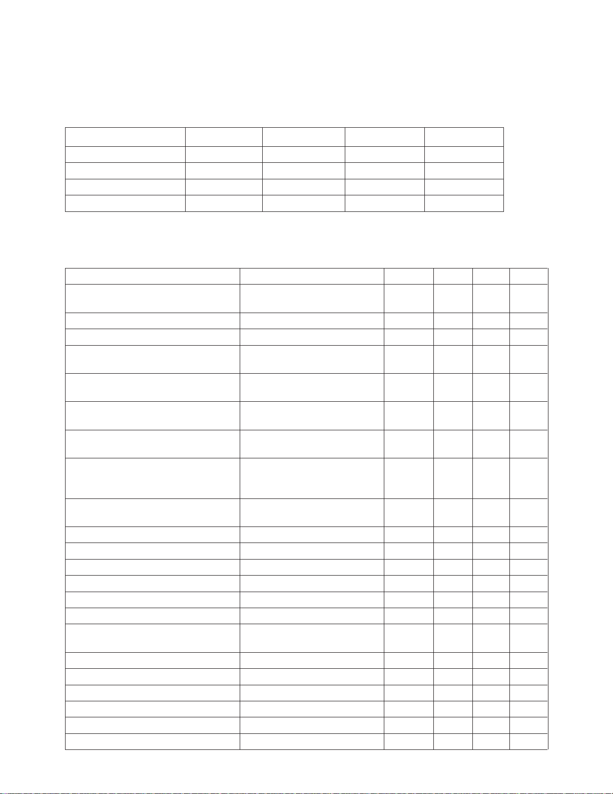
1. SQE Test: The FOIRL standard did not include the option of attaching a fiber transceiver to a DTE. Adding the SQE test to 10BASE-FL enables a 10BASE-FL transceiver to attach to a DTE.
2. 0 to at Least 2 Km Distance:
The FOIRL standard specifies a 1
km distance while 10BASE-FL
specifies 2 km. The additional 1
km distance for 10BASE-FL
comes from an increased flux
budget for the cable of 3.5 dB.
This 3.5 dB increase came from
an increase of 2.5 dB sensitivity
for the receiver and a 1 dB
improvement for the transmitter.
The following table illustrates the
transmit and receive power
requirements for the two
standards. Note: FOIRL specifies
optical power in peak and
10BASE-FL specifies it in
average. Subtracting 3 dB from
peak will give the average. In the
table below the FOIRL
specifications were converted
from peak to average power.
3. MAU State Diagrams are
Different: The state diagrams for
10BASE-FL are similar to
10BASE-T, while the state
diagrams for FOIRL are slightly
different. The differences are in
the AUI loopback, and in the link
integrity function.
Link Integrity - 10BASE-FL adds
an additional state to the Link
Integrity Test function that will
not allow an exit from the Low
Light State until both the
AUI Loopback - In 10BASE-FL
the DO to DI loopback is always
disabled during a collision, and
optical receive data is passed
transmitter and receiver are idle.
In FOIRL, it is possible to exit
from the Low Light State while
still receiving data.
through to DI. For FOIRL there
are some cases where loopback
continues (i.e. DO looped to DI)
during a collision, and others
where loopback is disabled
during a collision. 10BASE-FL is
identical to 10BASE-T in this
case. Please refer to the IEEE
standards for greater detail.
MAU Timing Differences - The
timing differences between
10BASE-FL and FOIRL relate to
propagation delays, start-up
delays, and collision deassert
delays. The following table
provides the details of these
parameters.
Timing FOIRL 10BASEFL
Parameter Differences (BIT Times) (BIT Times)
ORD input to input on DI
Steady State Prop Delay 0.5 2
Start-Up Delay 3.5 5
Output on DO to OTD_output
Steady State Prop Delay 0.5 2
Start-Up Delay 3.5 5
Collision Deassert to
SQE Deassert minimum 4.5 0
Transmit/Receive
Average Power Min. Max. Conditions
FOIRL
Transmitter -12 dBm -21 dBm
Receiver -12 dBm -30 dBm BER < 10
10BASE-FL
Transmitter -12 dBm -20 dBm
Receiver -12 dBm -32.5 dBm BER < 10
88
OTD - Optical Transmit Data
ORD - Optical Receive Data
DI, DO, CI - AU Interface Signals
-10
-9
Page 13

Timing Diagrams
t
TXNPW
T
X+
T
X-
VALID DATA
t
TXODY
t
TXSDY
t
TXFPW
TxOUT
R
R
t
TXLP
X+
X-
VALID DATA
VALID DATA
Figure 6. Transmit and Loopback Timing.
V
IN+
V
IN-
R
X+
R
X-
t
RXODY
VALID DATA
t
RXSDY
VALID DATA
t
AR
Figure 7. Receive Timing.
TxOUT
V
IN+
V
IN-
t
CPSQE
VALID DATA
VALID DATA
t
t
RXFX
AF
COL+
COL-
Rx+
Rx-
V
IN+
V
TxOUT
COL+
COL-
IN-
Tx Tx Rx Rx Rx
t
CPSQE
Figure 8. Collision Timing.
CS0
VALID DATA
VALID DATA
CS0
89
Page 14

V
IN+
V
IN-
TxOUT
COL+
COL-
Rx+
Rx-
VALID DATA
t
SQEXR
CS0
Rx
Rx Rx Tx Tx Tx
Figure 9. Collision Timing.
TxOUT
V
IN+
V
IN-
COL+
COL-
VALID DATA
t
SQEXR
CS0
Rx+
Rx-
RxIN
Figure 10. Collision Timing.
TxOUT
COL+
COL-
VALID DATA
Figure 11. SQE Timing.
90
RxIN RxIN
t
SQEDY
RxIN RxIN
1
t
CLF
t
SQETD
CS0
Page 15

Tx+
Tx-
VALID
DATA
TxOUT
COL+
COL-
Figure 12. Jabber Timing.
TxOUT
XMT
V
IN+
V
IN-
t
JAD
VALID DATA
t
LED
t
JSQE
CS0
t
t
LED
JRT
RCV
V
IN+
V
IN-
LMON
Figure 13. LED Timing.
t
LLPH
t
LLCL
91
 Loading...