

Page 1

DATA SH EET
Preliminary specification
File under Integrated Circuits, IC04
January 1995
INTEGRATED CIRCUITS
HEF4938B
Dual precision monostable
multivibrator
For a complete data sheet, please also download:
•The IC04 LOCMOS HE4000B Logic
Family Specifications HEF, HEC
•The IC04 LOCMOS HE4000B Logic
Package Outlines/Information HEF, HEC
Page 2
January 1995 2
Philips Semiconductors Preliminary specification
Dual precision monostable multivibrator HEF4938B
FEA TURES
• Separate reset inputs
• Triggering from leading or
trailing edge
• ICCcategory: MSI
DESCRIPTION
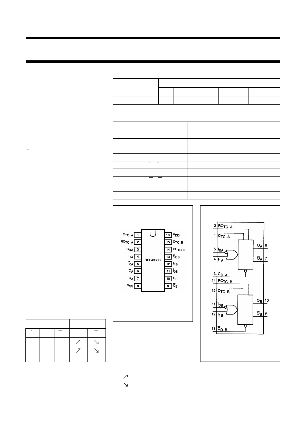
The HEF4938B is a dual
retriggerable-resettable monostable
multivibrator. Each multivibrator has
an active LOW trigger/retrigger input
(
I0), an active HIGH trigger/retrigger
input (I1), an overriding active LOW
direct reset input (CD), an output (O)
and its complement (O), and two pins
(CTCand RCTC) for connecting the
external timing components Ct and
Rt. Typical pulse width variation over
temperature range is ±0.2%.
The HEF4938B may be triggered by
either the positive or the negative
edges of the input pulse and will
produce an accurate output pulse
with a pulse width range of 10 µsto
infinity. The duration and accuracy of
the output pulse are determined by
the external timing components
Ctand Rt. The output pulse width (T)
is equal to Rt× Ct. The linear design
techniques in LOCMOS guarantee
precise control of the output pulse
width. A LOW level at CDterminates
the output pulse immediately.
Schmitt-trigger action in the inputs
makes the circuit highly tolerant for
slower rise and fall times.
FUNCTION TABLE
Notes
1. H = HIGH voltage level
2. L = LOW voltage level
INPUTS OUTPUTS
I
0
I
1
C
D
O O
↑ LH
H↑H
XXL L H
3. X = state is immaterial
4. ↑ = positive-going transition
5. ↓ = negative-going transition
6. = positive output pulse
7. = negative output pulse
ORDERING AND PACKAGE INFORMATION
PIN DESCRIPTION
TYPE NUMBER
PACKAGES
PINS PIN POSITION MATERIAL CODE
HEF4938B 16 DIL plastic SOT38Z
PIN NO. SYMBOL NAME AND FUNCTION
1, 15 C
TC A,CTC B
external capacitor connections
2, 14 RC
TC A
,RC
TC B
external capacitor/resistor connections
3, 13
CDA, C
DB
direct reset input (active LOW)
4, 12 I
1A,I1B
input (LOW-to-HIGH triggered)
5, 11
I0A, I
0B
input (HIGH-to-LOW triggered)
6, 10 O
A,OB
output
7, 9
OA, O
B
complementary output (active LOW)
8V
SS
ground (0 V)
16 V
DD
positive supply voltage
Fig.1 Pin configuration.
Fig.2 Functional diagram.
Page 3
January 1995 3
Philips Semiconductors Preliminary specification
Dual precision monostable multivibrator HEF4938B
This text is here in white to force landscape pages to be rotated correctly when browsing through the pdf in the Acrobat reader.This text is here in
_white to force landscape pages to be rotated correctly when browsing through the pdf in the Acrobat reader.This text is here inThis text is here in
white to force landscape pages to be rotated correctly when browsing through the pdf in the Acrobat reader. white to force landscape pages to be ...
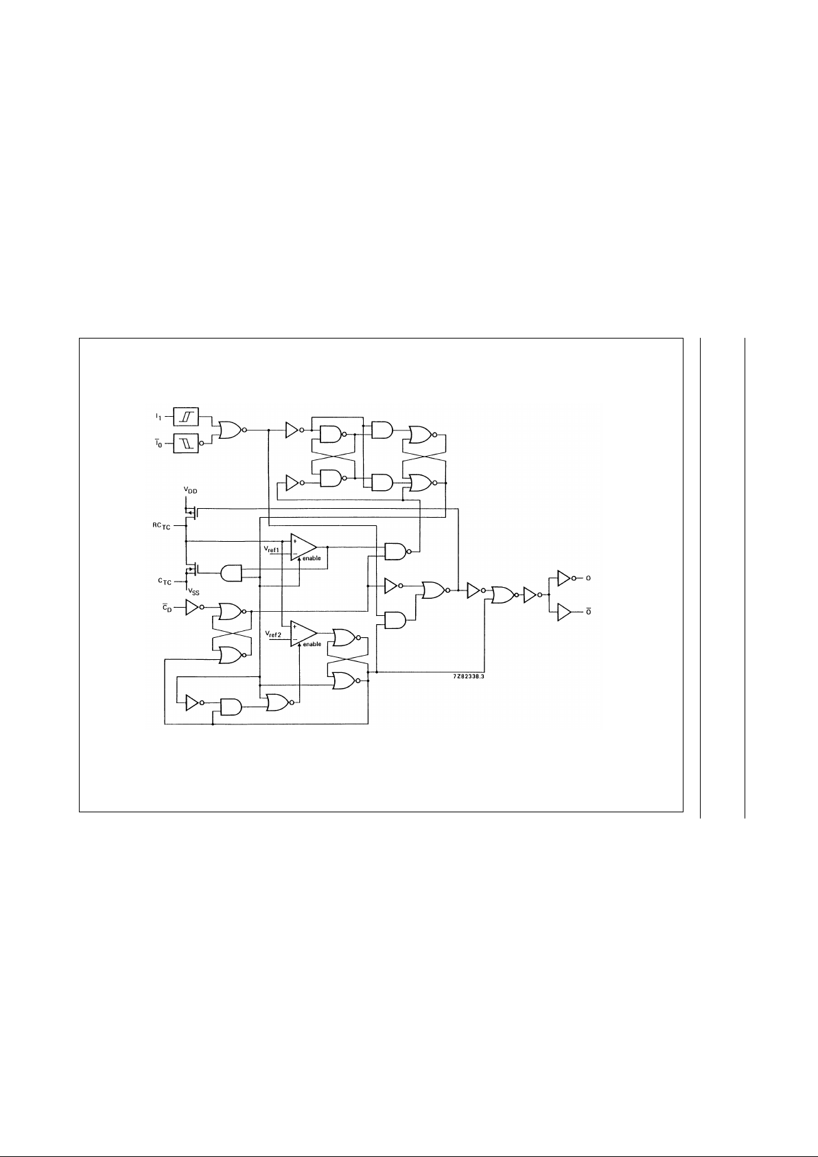
Fig.3 Logic diagram.
Page 4

January 1995 4
Philips Semiconductors Preliminary specification
Dual precision monostable multivibrator HEF4938B
FUNCTION TABLE
Notes
1. H = HIGH state (the more positive voltage)
2. L = LOW state (the less positive voltage)
3. X = state is immaterial
4. = positive-going transition
5. = negative-going transition
6. = positive output pulse
7. = negative output pulse
INPUTS OUTPUTS
I
0
I
1
C
D
O O
LH
HH
XX L L H
Fig.4 Connection of the external timing
components Rtand Ct.
DC CHARACTERISTICS
V
SS
=0 V
Note
1. Only one monostable is switching: current present during output pulse (output O is HIGH).
V
DD
V
SYMBOL
T
amb
(°C)
−40 + 25 + 85
TYP. MAX. TYP. MAX. TYP. MAX.
Supply current 5 55 µA
active state 10 I
D
150 µA
(see note) 15 220 µA
Input leakage
current 15 ±I
IN
300 1000 nA
(pins 2 and 14)
Page 5

January 1995 5
Philips Semiconductors Preliminary specification
Dual precision monostable multivibrator HEF4938B
AC CHARACTERISTICS
V
SS
= 0 V; T
amb
=25°C; CL= 50 pF; input transition times ≤ 20 ns.
PARAMETER
V
DD
(V)
SYMBOL MIN. TYP. MAX. UNIT
TYPICAL
EXTRAPOLATION
FORMULA
Propagation delay 5 − 200 460 173 ns + (0.55 ns/pF) C
L
I0, I1to O 10 t
PHL
− 90 180 ns 79 ns + (0.23 ns/pF) C
L
HIGH to LOW 15 − 60 120 52 ns + (0.16 ns/pF) C
L
Propagation delay 5 − 220 440 193 ns + (0.55 ns/pF) C
L
I0,I1to O10t
PLH
− 85 190 ns 74 ns + (0.23 ns/pF) C
L
LOW to HIGH 15 − 60 120 52 ns + (0.16 ns/pF) C
L
Propagation delay 5 − 125 250 98 ns + (0.55 ns/pF) C
L
CDto O 10 t
PHL
− 55 110 ns 44 ns + (0.23 ns/pF) C
L
HIGH to LOW 15 − 40 80 32 ns + (0.16 ns/pF) C
L
Propagation delay 5 − 125 250 98 ns + (0.55 ns/pF) C
L
CDto O 10 t
PLH
− 55 110 ns 44 ns + (0.23 ns/pF) C
L
LOW to HIGH 15 − 40 80 32 ns + (0.16 ns/pF) C
L
Recovery times
CDto I0, I
1
5 − 20 40
10 t
RCD
− 10 20 ns
15 − 510
Retrigger times 5 0 −−
O,
OtoI0,I
1
10 t
RO
0 −−ns
LOW to OFF 15 0 −−
Minimum output 5 90 45 −
pulse width LOW 10 t
WIOL
30 15 − ns
I
0
15 24 12 −
Minimum output 5 50 25 −
pulse width LOW 10 t
WI1H
24 12 − ns
I
1
15 20 10 −
Output pulse width
O, O
5 9.3 10.0 10.6
10 t
WO
9.2 9.9 10.5 ms Rt= 100 kΩ;Ct= 100 nF
15 9.1 9.8 10.4
Page 6

January 1995 6
Philips Semiconductors Preliminary specification
Dual precision monostable multivibrator HEF4938B
AC CHARACTERISTICS
V
SS
= 0 V; T
amb
=25°C; CL= 50 pF; input transition times ≤ 20 ns
Note
1. The maximum permissible resistance R
t
, which holds the specified accuracy of tWO, depends on the leakage current
of the capacitor Ctand the leakage of the HEF4538B.
V
DD
V
SYMBOL MIN. TYP. MAX.
Change in output O 5 ± 0,2 %
pulse width over 10 ∆t
WO
± 0,2 %
temperature (T
amb
)15 ±0,2 %
Change in output O
pulse width over ∆t
WO
± 1,5 %
V
DD
range 5 to 15 V
Pulse width variation 5 ± 1%
R
t
= 100 kΩ
Ct= 2 nF to 10 µF
between circuits 10 ∆t
WO
± 1%
in same package 15 ± 1%
External timing
resistor R
t
5 −
(1)
kΩ
External timing
capacitor C
t
2000 − no limits pF
Input capacitance
(pin 2 or 14) C
IN
15 pF
Page 7

January 1995 7
Philips Semiconductors Preliminary specification
Dual precision monostable multivibrator HEF4938B
Fig.5 Waveforms showing minimum I0,I1, O and CDpulse widths, recovery times and propagation delays.
Page 8

January 1995 8
Philips Semiconductors Preliminary specification
Dual precision monostable multivibrator HEF4938B
This text is here in white to force landscape pages to be rotated correctly when browsing through the pdf in the Acrobat reader.This text is here in
_white to force landscape pages to be rotated correctly when browsing through the pdf in the Acrobat reader.This text is here inThis text is here in
white to force landscape pages to be rotated correctly when browsing through the pdf in the Acrobat reader. white to force landscape pages to be ...
Fig.6 Timing diagram.
(1) Positive edge triggering.
(2) Positive edge re-triggering (pulse lengthening).
(3) Negative edge triggering.
(4) Reset (pulse shortening).
(5) T = Rt× Ct.
 Loading...