

Page 1
INTEGRATED CIRCUITS
DATA SH EET
For a complete data sheet, please also download:
•The IC04 LOCMOS HE4000B Logic
Family Specifications HEF, HEC
•The IC04 LOCMOS HE4000B Logic
Package Outlines/Information HEF, HEC
HEF4750V
LSI
Frequency synthesizer
Product specification
File under Integrated Circuits, IC04
January 1995
Page 2

Philips Semiconductors Product specification
Frequency synthesizer
DESCRIPTION
The HEF4750V frequency synthesizer is one of a pair of
LOCMOS devices, primarily intended for use in
high-performance frequency synthesizers, e.g. in all
communication, instrumentation, television and broadcast
applications. A combination of analogue and digital
techniques results in an integrated circuit that enables high
performance. The complementary device is the universal
divider type HEF4751V.
Together with a standard prescaler, the two LOCMOS
integrated circuits offer low-cost single loop synthesizers
with full professional performance. Salient features offered
(in combination with HEF4751V) are:
• Wide choice of reference frequency using a single
crystal.
• High-performance phase comparator low phase
noise low spurii.
• System operation to > 1 GHz.
• Typical 15 MHz input at 10 V.
• Flexible programming:
frequency offsets
ROM compatible
fractional channel capability.
1
• Programme range 6
3 decades of prescaler control.
• Division range extension by cascading.
• Built-in phase modulator.
• Fast lock feature.
• Out-of-lock indication.
• Low power dissipation and high noise immunity.
⁄2 decades, including up to
HEF4750V
LSI
SUPPLY VOLTAGE
RATING RECOMMENDED OPERATING
−0,5 to +15 9,5 to 10,5 V
APPLICATION INFORMATION
Some examples of applications for the HEF4750V in
combination with the HEF4751V are:
• VHF/UHF mobile radios.
• HF s.s.b. transceivers.
• Airborne and marine communications and navaids.
• Broadcast transmitters.
• High quality radio and television receivers.
• High performance citizens band equipment.
• Signal generators.
January 1995 2
Page 3
Philips Semiconductors Product specification
Frequency synthesizer
HEF4750V
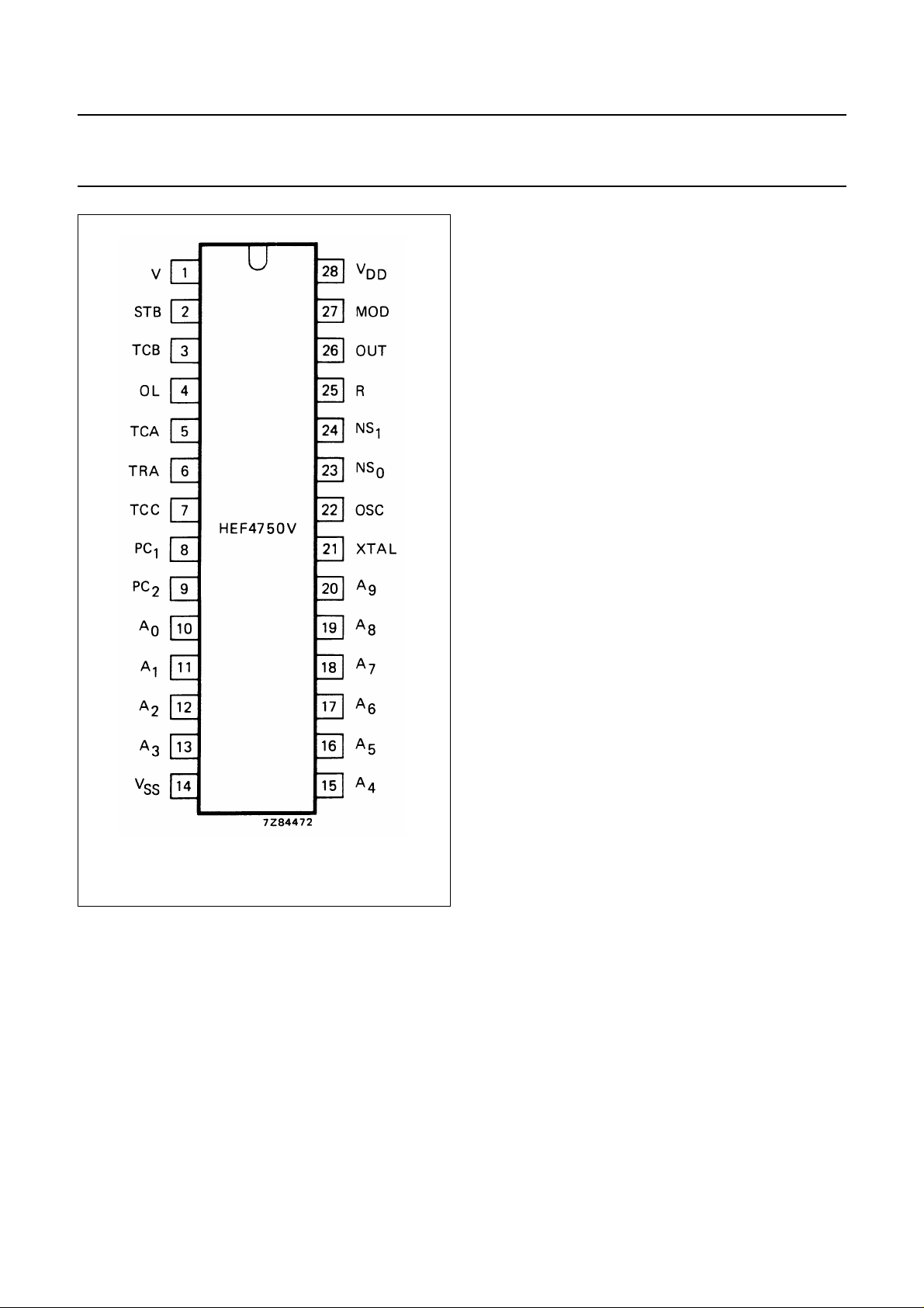
PINNING
R phase comparator input, reference
V phase comparator input
STB strobe input
TCA timing capacitor C
TCB timing capacitor C
TCC timing capacitor C
TRA biasing pin (resistor R
PC
PC
1
2
analogue phase comparator output
digital phase comparator output
MOD phase modulation input
OL out-of-lock indication
OSC reference oscillator/buffer input
XTAL reference oscillator/buffer output
A
to A
0
NS
, NS1programming inputs, prescaler
0
programming inputs/programmable divider
9
OUT reference divider output
pin
A
pin
B
pin
C
)
A
LSI
Fig.1 Pinning diagram.
HEF4750VD(F): 28-lead DIL; ceramic (cerdip)
(SOT135)
( ): Package Designator North America
January 1995 3
Page 4
This text is here in white to force landscape pages to be rotated correctly when browsing through the pdf in the Acrobat reader.This text is here in
_white to force landscape pages to be rotated correctly when browsing through the pdf in the Acrobat reader.This text is here inThis text is here in
white to force landscape pages to be rotated correctly when browsing through the pdf in the Acrobat reader. white to force landscape pages to be ...
January 1995 4
Philips Semiconductors Product specification
Frequency synthesizer
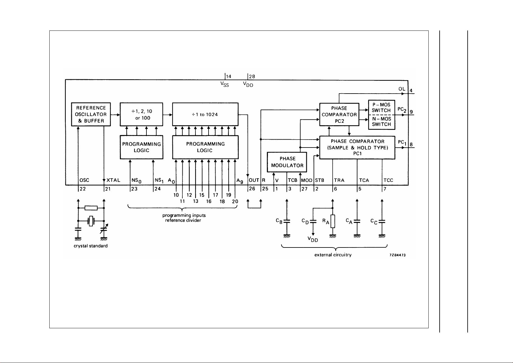
N.B. PC1= analogue output; PC2= 3-state output.
Fig.2 Block diagram comprising five basic functions: phase comparator 1 (PC1), phase comparator 2 (PC2), phase modulator, reference
oscillator and reference divider. These functions are described separately.
HEF4750V
LSI
Page 5
Philips Semiconductors Product specification
Frequency synthesizer
FUNCTIONAL DESCRIPTION
Phase comparator 1
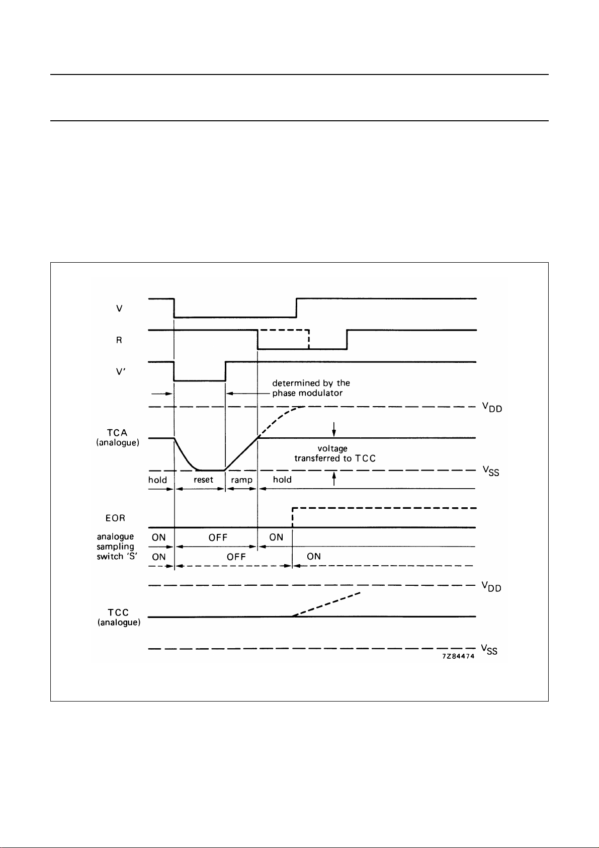
Phase comparator 1 (PC1) is built around a SAMPLE and
HOLD circuit. A negative-going transition at the V-input
causes the hold capacitor (C
a specified delay, caused by the Phase Modulator by
means of an internal V’ pulse, it produces a positive-going
ramp. A negative-going transition at the R-input terminates
) to be discharged and after
A
HEF4750V
LSI
the ramp. Capacitor C
has attained. Via an internal sampling switch this voltage
is transferred to CCand in turn buffered and made
available at output PC1.
If the ramp terminates before an R-input is present, an
internal end of ramp (EOR) signal is produced.
These actions are illustrated in Fig.3.
holds the voltage that the ramp
A
Fig.3 Waveforms associated with PC1.
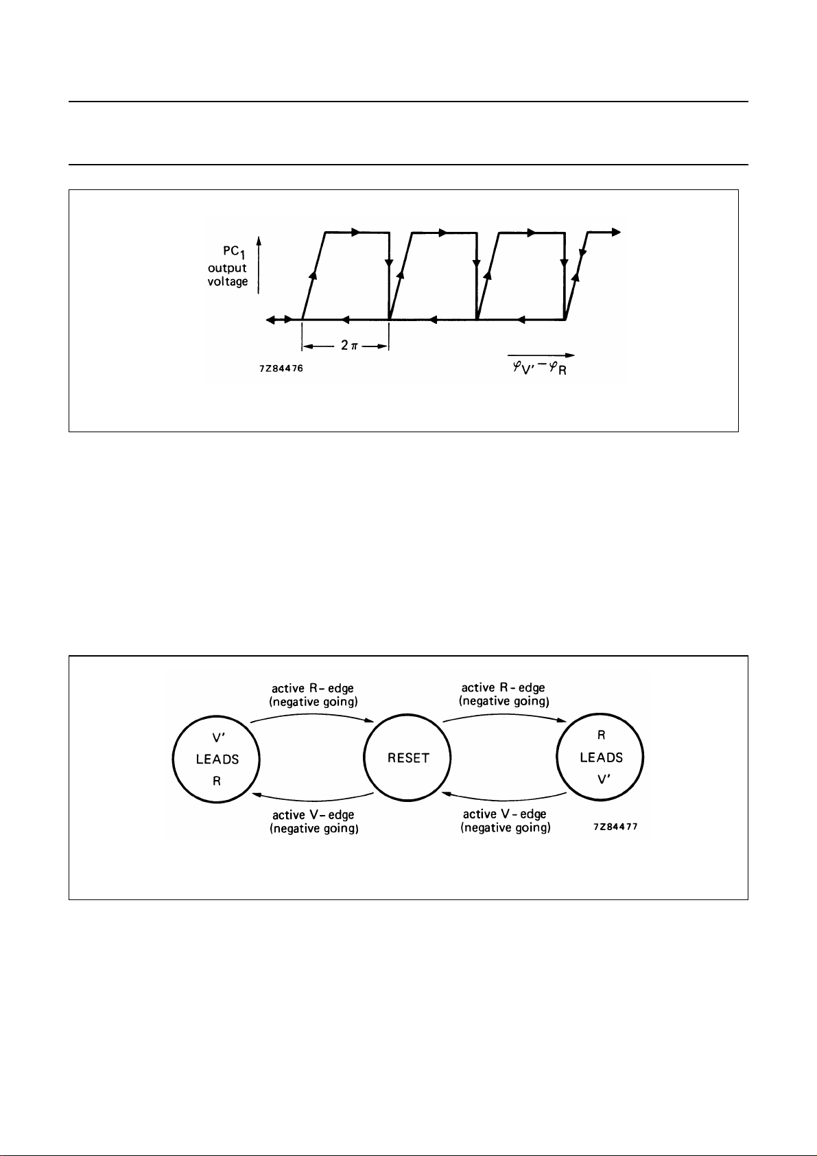
The resultant phase characteristic is shown in Fig.4.
January 1995 5
Page 6
Philips Semiconductors Product specification
Frequency synthesizer
Fig.4 Phase characteristic of PC1.
PC1 is designed to have a high gain, typically 3200 V/cycle
(at 12,5 kHz). This enables a low noise performance.
Phase comparator 2
Phase comparator 2 (PC2) has a wide range, which
enables faster lock times to be achieved than otherwise
would be possible. It has a linear ± 360° phase range,
which corresponds to a gain of typically 5 V/cycle.
HEF4750V
LSI
This digital phase comparator has three stable states:
• reset state,
• V’ leads R state,
• R leads V’ state.
Fig.5 State diagram of PC2.
Output PC2produces positive or negative-going pulses
with variable width; they depend on the phase relationship
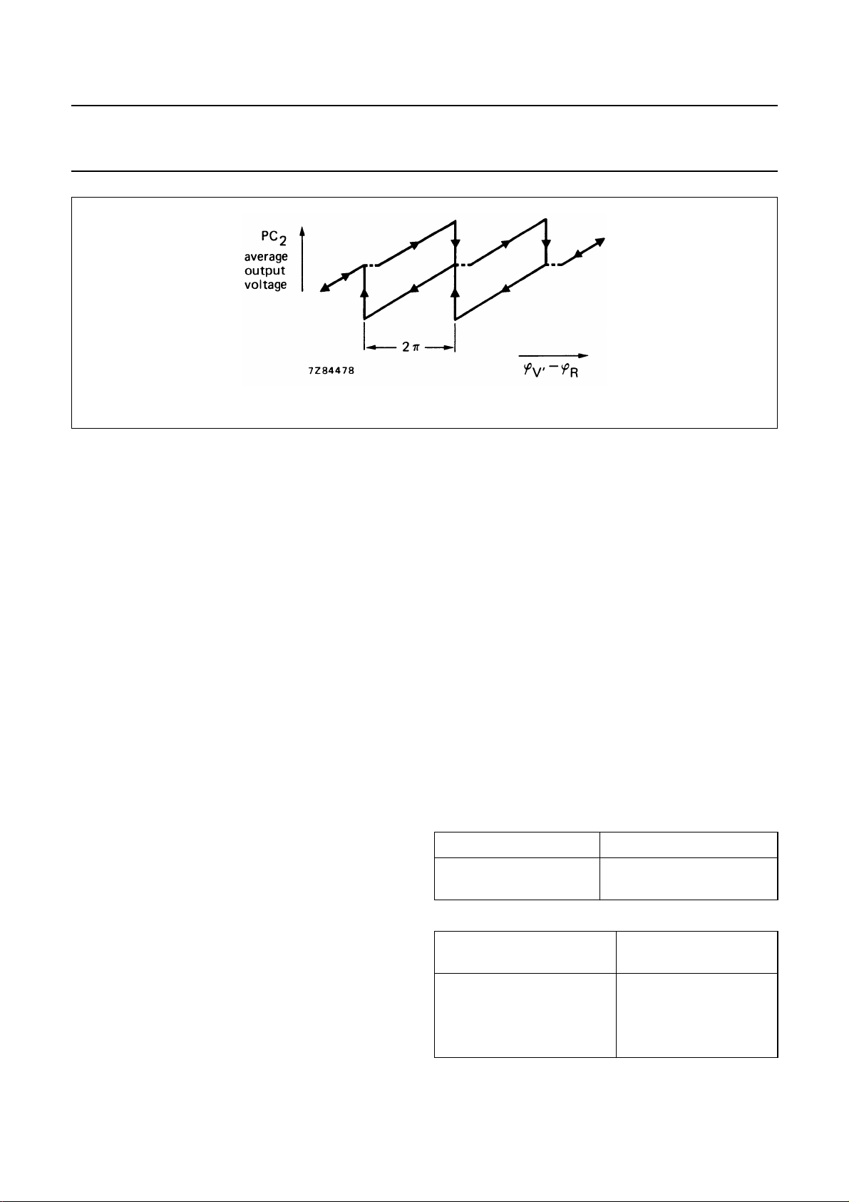
of R and V’. The average output voltage is a linear function
of the phase difference. Output PC2remains in the high
impedance OFF-state in the region in which PC1 operates.
The resultant phase characteristic is shown in Fig.6.
Conversion from one state to another takes place
according to the state diagram of Fig.5.
January 1995 6
Page 7
Philips Semiconductors Product specification
Frequency synthesizer
Fig.6 Phase characteristic of PC2.
Strobe function
The strobe function is intended for applications requiring
extremely fast lock times. In normal operation the
additional strobe input (STB) can be connected to the
V-input and the circuit will function as described in the
previous sections.
In single, phase-locked-loop type frequency synthesizers,
the comparison frequency generally used is either the
nominal channel spacing or a sub-multiple. PC2 runs at
the higher frequency (a higher reference frequency must
also be used), whilst strobing takes place on the lower
frequency, thereby obtaining a decrease in lock time. In a
system using the Universal Divider HEF4751V, the output
OFS cycles on the lower frequency, the output OFF cycles
on the higher frequency.
HEF4750V
LSI
way. If no modulation is required, the MOD-input must be
connected to a fixed voltage of a certain positive value up
. Care must be taken that the V’ pulse is never
to V
DD
smaller than the minimum value to ensure that the external
capacitor of PC1 (CA) can be discharged during that time.
Since the V’ pulse width is directly related to the TCB ramp
duration, there is a requirement for the minimum value of
this ramp duration.
Reference oscillator
The reference oscillator normally operates with an external
crystal as shown in Fig.2. The internal circuitry can be
used as a buffer amplifier in case an external reference
should be required.
Reference divider
Out-of-lock function
There are a number of situations in which the system goes
from the locked to the out-of-lock state (OL goes HIGH):
1. When V’ leads R, however out of the range of PC1.
2. When R leads V’.
3. When an R-pulse is missing.
4. When a V-pulse is missing.
5. When two successive STB-commands occur, the first
without corresponding V-signal.
Phase modulator
The phase modulator only uses one external capacitor,
at pin TCB. A negative-going transition at the V-input
C
B
causes CBto produce a positive-going linear ramp. When
the ramp has reached a value almost equal to the
modulation input voltage (at MOD), the ramp terminates,
CBdischarges and a start signal to the CA-ramp at TCA is
produced. A linear phase modulation is reached in this
January 1995 7
The reference divider consists of a binary divider with a
programmable division ratio of 1 to 1024 and a prescaler
with selectable division ratios of 1, 2, 10 and 100,
according to the following tables:
Binary divider
N (A
TO A9) DIVISION RATIO
0
0 1024
0 ≤ N ≤ 1023 N
Prescaler
PROGRAMMING WORD
, NS1)
(NS
0
01
12
210
3 100
DIVISION RATIO
Page 8
Philips Semiconductors Product specification
Frequency synthesizer
In this way suitable comparison frequencies can be
obtained from a range of crystal frequencies. The divider
can also be used as a ‘stand alone’ programmable divider
by connecting input TRA to VDD, which causes all internal
analogue currents to be switched off.
Biasing circuitry
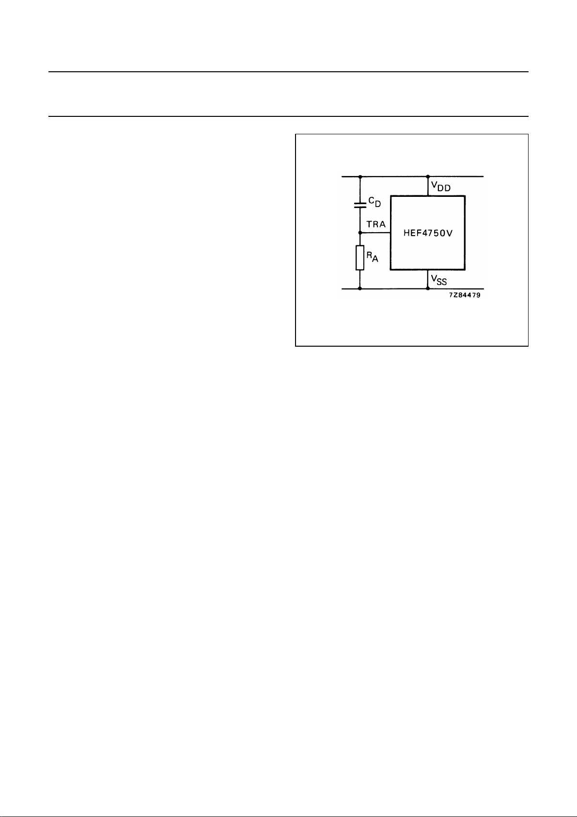
The biasing circuitry uses an external current source or
resistor, which has to be connected between the TRA and
V
pins. This circuitry supplies all analogue parts of the
SS
circuit. Consequently the analogue properties of the
device, such as gain, charge currents, speed, power
dissipation, impedance levels etc., are mainly determined
by the value of the input current at TRA. The TRA input
must be decoupled to V
CDhas to be chosen such that the TRA input is ‘clean’, e.g.
10 nF at RA= 68 kΩ.
, as shown in Fig.7. The value of
DD
HEF4750V
LSI
Fig.7 Decoupling of input TRA.
RATINGS
Limiting values in accordance with the Absolute Maximum System (IEC 134)
Supply voltage V
Voltage on any input V
DD
I
−0,5 to + 15 V
−0,5 to VDD+ 0,5 V
D.C. current into any input or output ± I max. 10 mA
Power dissipation per package
for T
= 0 to + 85 °CP
amb
tot
max. 500 mW
Power dissipation per output
for T
Storage temperature T
Operating ambient temperature T
= 0 to 85 °C P max. 100 mW
amb
stg
amb
−65 to + 150 °C
−40 to + 85 °C
January 1995 8
Page 9
Philips Semiconductors Product specification
Frequency synthesizer
HEF4750V
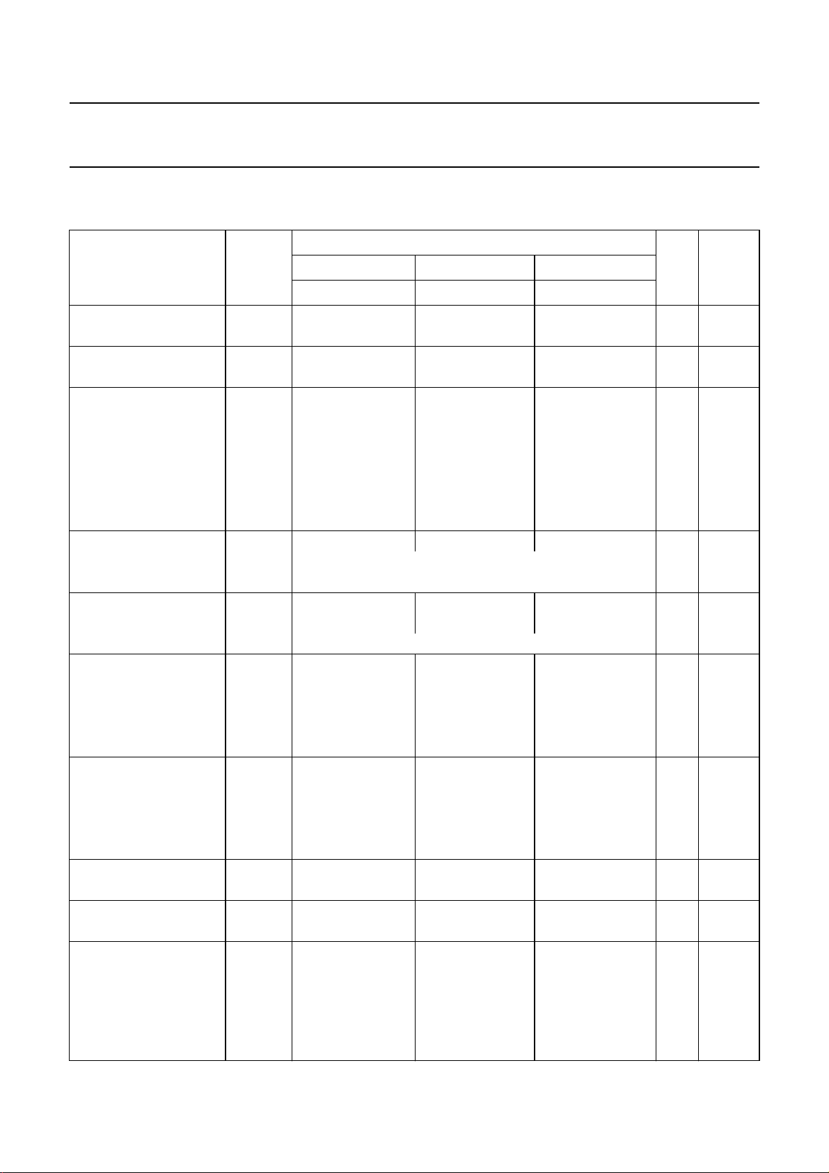
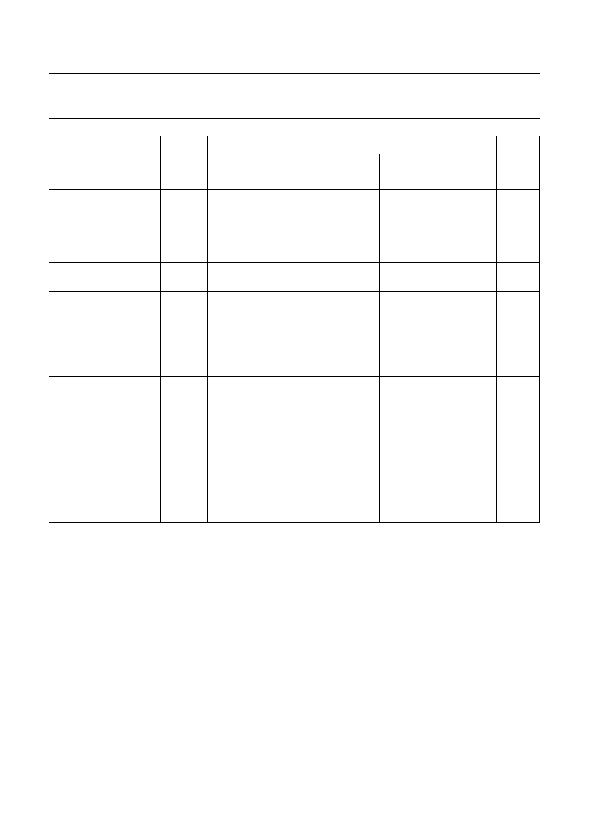
DC CHARACTERISTICS
at V
= 10 V ± 5%; voltages are referenced to VSS= 0 V, unless otherwise specified; for definitions see note 1.
DD
T
(°C
amb
PARAMETER SYMBOL
MIN. TYP. MAX. MIN. TYP. MAX. MIN. TYP. MAX.
Quiescent device
current I
DD
−− 100 −− 100 −− 750 µA2
Input current; logic
inputs, MOD ± I
IN
−− 300 −− 300 −− 1000 nA 3
Output leakage current
at1⁄2V
DD
TCA, hold-state ± I
Z
−− 20 − 0,05 20 −− 60 nA
TCC, analogue
switch OFF ± I
PC
, high impedance
2
OFF-state ± I
Z
Z
−− 20 − 0,05 20 −− 60 nA
−− 50 −− 50 −− 500 nA
Logic input voltage
LOW V
HIGH V
IL
IH
max. 0,3 VDD V
max. 0,7 VDD V
Logic output voltage
LOW; at I
HIGH V
<1µAV
O
OL
OH
−− 50 −− 50 −− 50 mV 3
min. VDD− 50 mV mV 3
Logic output current
LOW; at VOL= 0,5 V 3
outputs OL, PC
OUT I
output XTAL I
,
2
OL
OL
5,5 −−4,6 −−3,6 −−mA
2,8 −−2,4 −−1,9 −−mA
Logic output current
HIGH;
at V
OH=VDD
outputs OL, PC
output XTAL −I
− 0,5 V 3
,OUT −I
2
OH
OH
1,5 −−1,3 −−1,0 −−mA
1,4 −−1,2 −−0,9 −−mA
Output TCC sink
current I
O
−− −−2,1 −− − −mA 3,4,5
Output TCC source
current −I
O
−− −−1,9 −− − −mA 3,4,6
Internal resistance
of TCC
output swing
≤ 200 mV
specified output range:
0,3 V
DD
to 0,7 V
DDRi
−− −−0,7 −− − −kΩ 3,4
UNIT NOTES−40 + 25 + 85
LSI
3,4
January 1995 9
Page 10
Philips Semiconductors Product specification
Frequency synthesizer
HEF4750V
T
(°C
amb
PARAMETER SYMBOL
MIN. TYP. MAX. MIN. TYP. MAX. MIN. TYP. MAX.
Output TCC voltage
with respect to
TCA input voltage ∆V − 0 −− 0 −− 0 −V 3,4,7
Output PC
current I
Output PC
current −I
sink
1
source
1
O
O
−− −−1,1 −− − −mA 3,4,8
−− −−1,0 −− − −mA 3,4,9
Internal resistance
of PC
1
output swing
≤ 200 mV
specified output range:
0,3 V
Output PC
to 0,7 V
DD
voltage
1
DDRi
−− −−1,4 −− − −kΩ 3,4
with respect to
TCC input voltage ∆V − 0 −− 0 −− 0 −V 3,4,10
EOR generation
V
EOR=VDD
− V
TCA
V
EOR
− 0,9 −− 0,7 −− 0,6 − V 3,4,11
Source current; HIGH
at V
OUT
=1⁄2VDD;
output in ramp mode 3,4
TCA I
TCB I
O
O
−− −−13 −− − −mA
−− −−2,5 −− − −mA
UNIT NOTES−40 + 25 + 85
LSI
January 1995 10
Page 11
Philips Semiconductors Product specification
Frequency synthesizer
HEF4750V
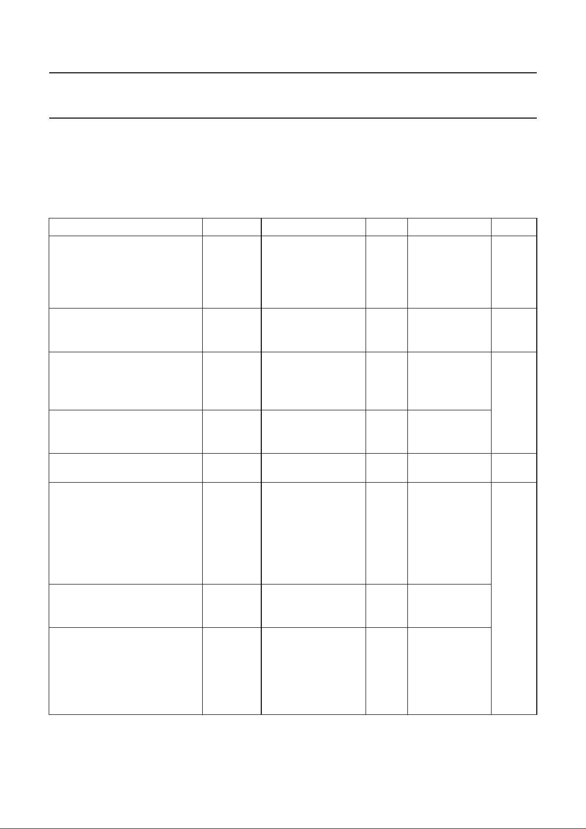
AC CHARACTERISTICS
General note
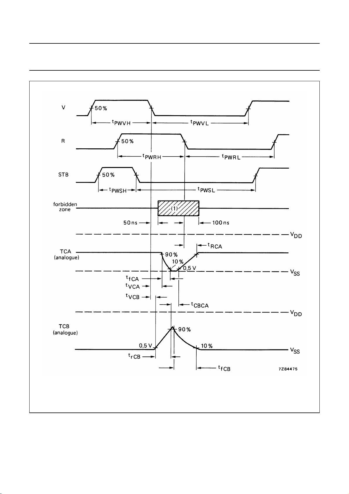
The dynamic specifications are given for the circuit built-up with external components as given in Fig.8, under the
following conditions; for definitions see note 1; for definitions of times see Fig.19; V
transition times ≤ 20 ns; R
= 68 kΩ±30% (see also note 4); CA= 270 pF; CB= 150 pF; CC= 1 nF; CD= 10 nF; unless
A
otherwise specified.
SYMBOL MIN. TYP. MAX. UNIT CONDITIONS NOTES
Slew rate
TCA S
TCA S
TCB S
TCB S
TCA
TCA
TCB
TCB
− 52 − V/µsR
− 28 − V/µsR
− 20 − V/µsR
− 10 − V/µsR
Ramp linearity
TCA I
TCB I
Start of TCA-ramp delay t
Delay of TCA-hold t
Delay of TCA-discharge t
Start of TCB-ramp delay t
TCB-ramp duration t
TCA
TCB
CBCA
RCA
VCA
VCB
rCB
t
rCB
t
rCB
− 2 − %13
− 2 − %13
− 200 − ns
− 40 − ns
− 60 − ns
− 60 − ns
− 250 − ns V
− 350 − ns V
− 450 − ns V
Required TCB min.
ramp duration t
rCB
− 150 − ns 14
Pulse width
V : LOW t
V : HIGH t
R : LOW t
R : HIGH t
STB : LOW t
STB : HIGH t
PWVL
PWVH
PWRL
PWRH
PWSL
PWSH
− 20 − ns
− 20 − ns
− 20 − ns
− 20 − ns
− 20 − ns
− 20 − ns
Fall time
TCA t
TCB t
Prescaler input frequency f
Binary divider frequency f
Crystal oscillator frequency f
fCA
fCB
PR
DIV
OSC
− 50 − ns
− 50 − ns
− 30 − MHz all division ratios
− 30 − MHz all division ratios
− 10 − MHz
Average power supply current locked state
with speed-up 1 : 10 I
without speed-up I
P
P
− 3,6 − mA 15
− 3,2 − mA 16
= 10 V ± 5%; T
DD
= minimum 12
A
= maximum 12
A
= minimum 12
A
= maximum 12
A
MOD
MOD
MOD
=4V
=6V
=8V
=25°C; input
amb
LSI
January 1995 11
Page 12

Philips Semiconductors Product specification
Frequency synthesizer
HEF4750V
LSI
Notes
1. Definitions:
RA= external biasing resistor between pins TRA and VSS; 68 kΩ±30%.
CA= external timing capacitor for time/voltage converter, between pins TCA and VSS.
CB= external timing capacitor for phase modulator, between pins TCB and VSS.
CC= external hold capacitor between pins TCC and VSS.
CD= decoupling capacitor between pins TRA and VDD.
Logic inputs: V, R, STB, A0to A9, NS0, NS1, OSC.
Logic outputs: OL, PC2, XTAL, OUT.
Analogue signals: TCA, TCB, TCC, TRA, PC1, MOD.
2. TRA at VDD; TCA, TCB, TCC and MOD at VSS; logic inputs at VSSor VDD.
3. All logic inputs at VSSor VDD.
4. RAconnected; its value chosen such that I
5. The analogue switch is in the ON position (see Fig.9).
6. The analogue switch is in the ON position (see Fig.10).
7. See Fig.11.
This guarantees the d.c. voltage gain, combined with d.c.-offset.
Input condition: 0,3 VDD≤ V
∆V=V
TCC−VTCA
.
TCA
≤ 0,7 VDD.
8. See Fig.12.
9. See Fig.13.
10. See Fig.14.
This guarantees the d.c. voltage gain, combined with d.c.-offset.
Input condition: 0,3 VDD≤ V
∆V=V
PC1−VTCC
.
TCC
≤ 0,7 VDD.
11. Switching level at TCA, generating an EOR-signal, during increasing input voltage.
12. See Fig.15.
13. See Fig.16.
Definition of the ramp linearity at full swing.
14. The external components and modulation input voltage must be chosen such that this requirement will be fulfilled, to
ensure that CAis sufficiently discharged during that time.
15. See Fig.17.
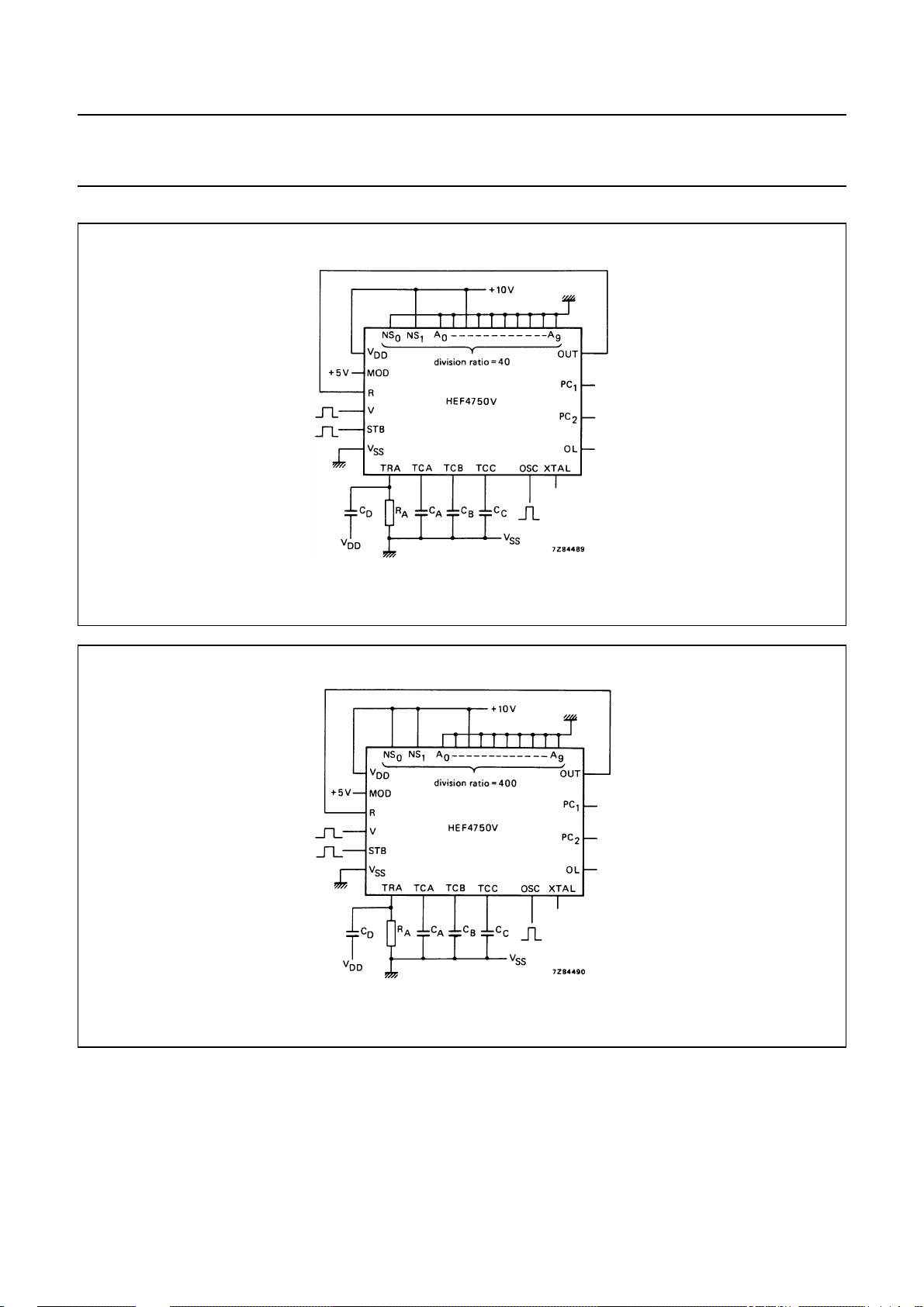
Circuit connections for power supply current specification, with speed-up 1 : 10. V and R are in the range of PC1,
such that the output voltage at PC1is equal to 5 V.
f
= 5 MHz (external clock)
OSC
f
= 12,5 kHz
STB
fV= 125 kHz
16. See Fig.18.
Circuit connections for power supply current specification, without speed-up. V and R are in the range of PC1, such
that the output voltage at PC1is equal to 5 V.
f
= 5 MHz (external clock)
OSC
f
= 12,5 kHz
STB
fV= 12,5 kHz
= 100 µA.
TRA
January 1995 12
Page 13
Philips Semiconductors Product specification
Frequency synthesizer
HEF4750V
LSI
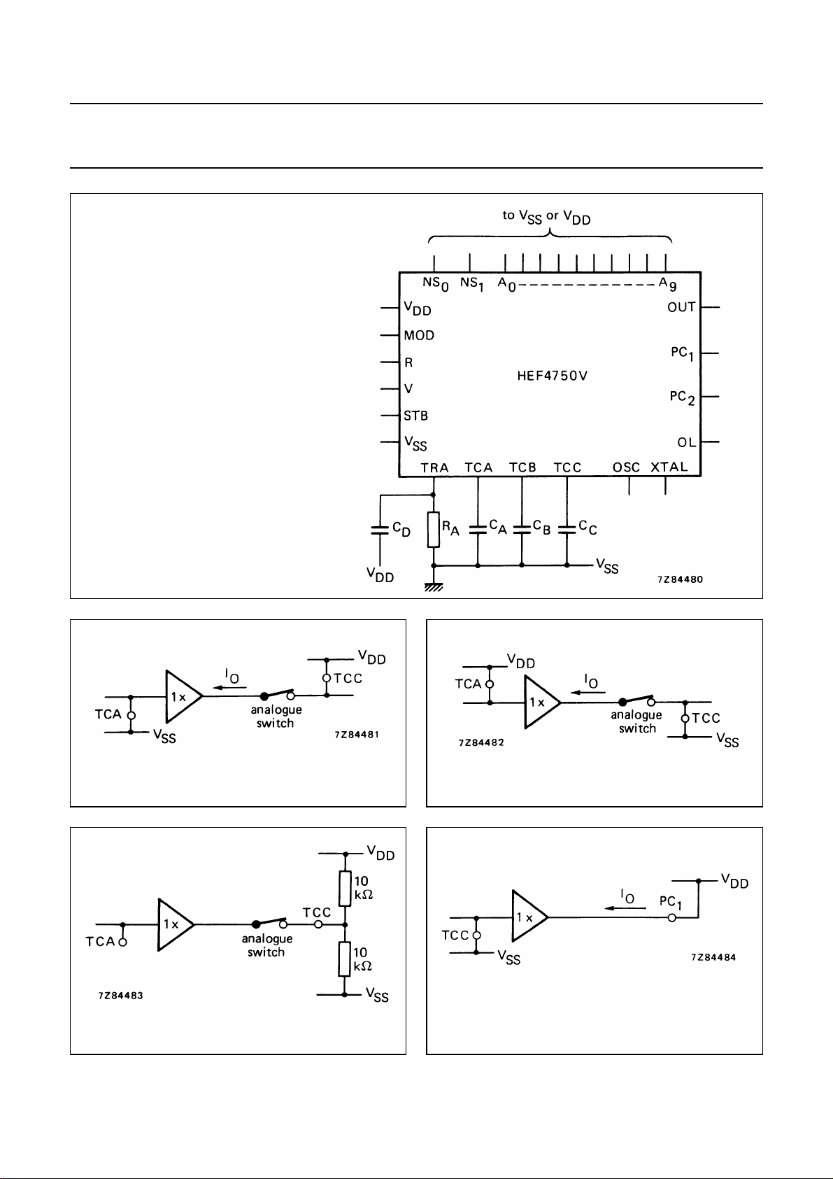
Fig.8 Test circuit for measuring a.c.
characteristics.
Fig.9 Equivalent circuit for note 5. Fig.10 Equivalent circuit for note 6.
Fig.11 Circuit for note 7. Fig.12 Equivalent circuit for PC1sink current.
January 1995 13
Page 14
Philips Semiconductors Product specification
Frequency synthesizer
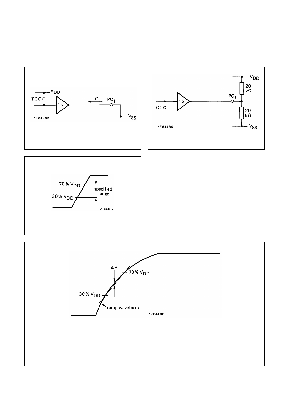
Fig.13 Equivalent circuit for PC1source current. Fig.14 Circuit for note 10.
HEF4750V
LSI
Fig.15 Waveform at the output.
Linearity
--------------------- -
1/2V
DD
100× %.=
∆V
Fig.16 Definition of the ramp linearity at full swing.
∆V is the maximum deviation of the ramp waveform to the straight line, which joins the 30% VDDand
70% VDDpoints.
January 1995 14
Page 15
Philips Semiconductors Product specification
Frequency synthesizer
HEF4750V
LSI
Fig.17 Circuit for note 15.
Fig.18 Circuit for note 16.
January 1995 15
Page 16
Philips Semiconductors Product specification
Frequency synthesizer
HEF4750V
LSI
(1) Forbidden zone in the
January 1995 16
locked state
for the positive edge of V and R and both edges of STB.
Fig.19 Waveforms showing times in the locked state.
Page 17
Philips Semiconductors Product specification
Frequency synthesizer
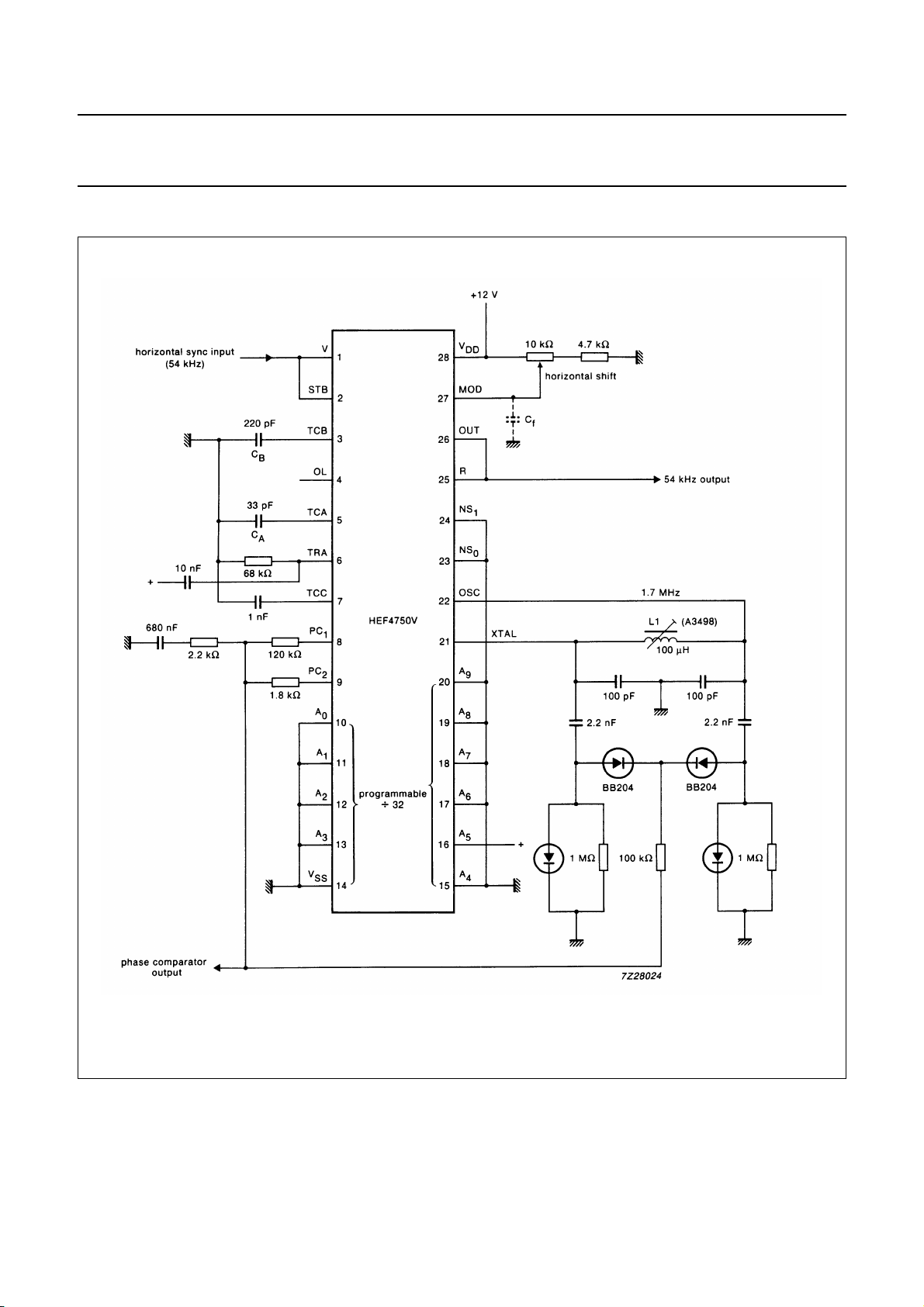
APPLICATION INFORMATION
HEF4750V
LSI
Fig.20 Application of HEF4750V as horizontal sync circuit with Phase-Locked Loop (PLL) and LC oscillator with
vari-cap control.
January 1995 17
 Loading...