

Page 1

INTEGRATED CIRCUITS
DATA SH EET
For a complete data sheet, please also download:
•The IC04 LOCMOS HE4000B Logic
Family Specifications HEF, HEC
•The IC04 LOCMOS HE4000B Logic
Package Outlines/Information HEF, HEC
HEF4894B
12-stage shift-and-store register
LED driver
Product specification
File under Integrated Circuits, IC04
January 1995
Page 2
Philips Semiconductors Product specification
12-stage shift-and-store register LED driver HEF4894B
APPLICATIONS
• Automotive
• Industrial
GENERAL DESCRIPTION
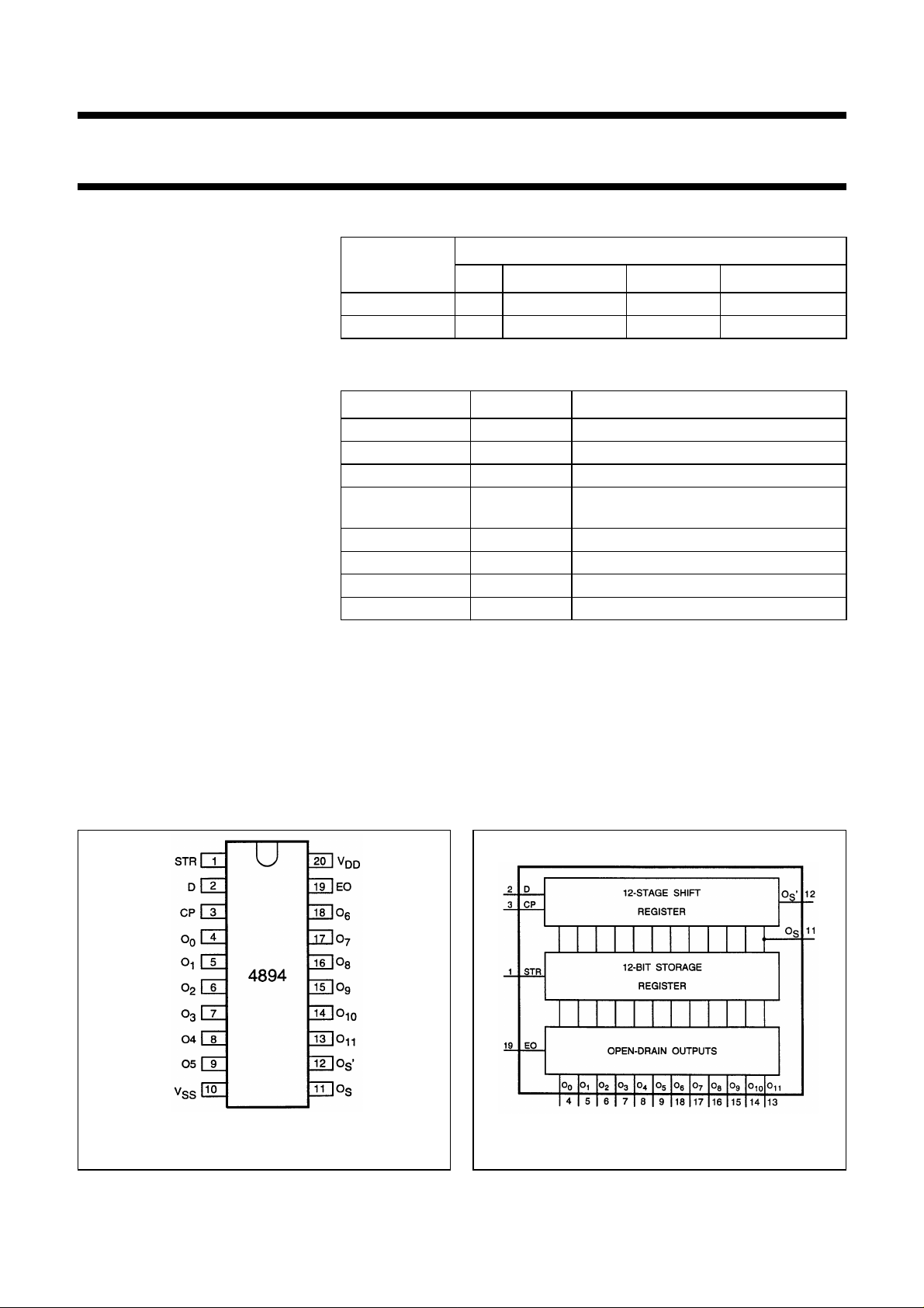
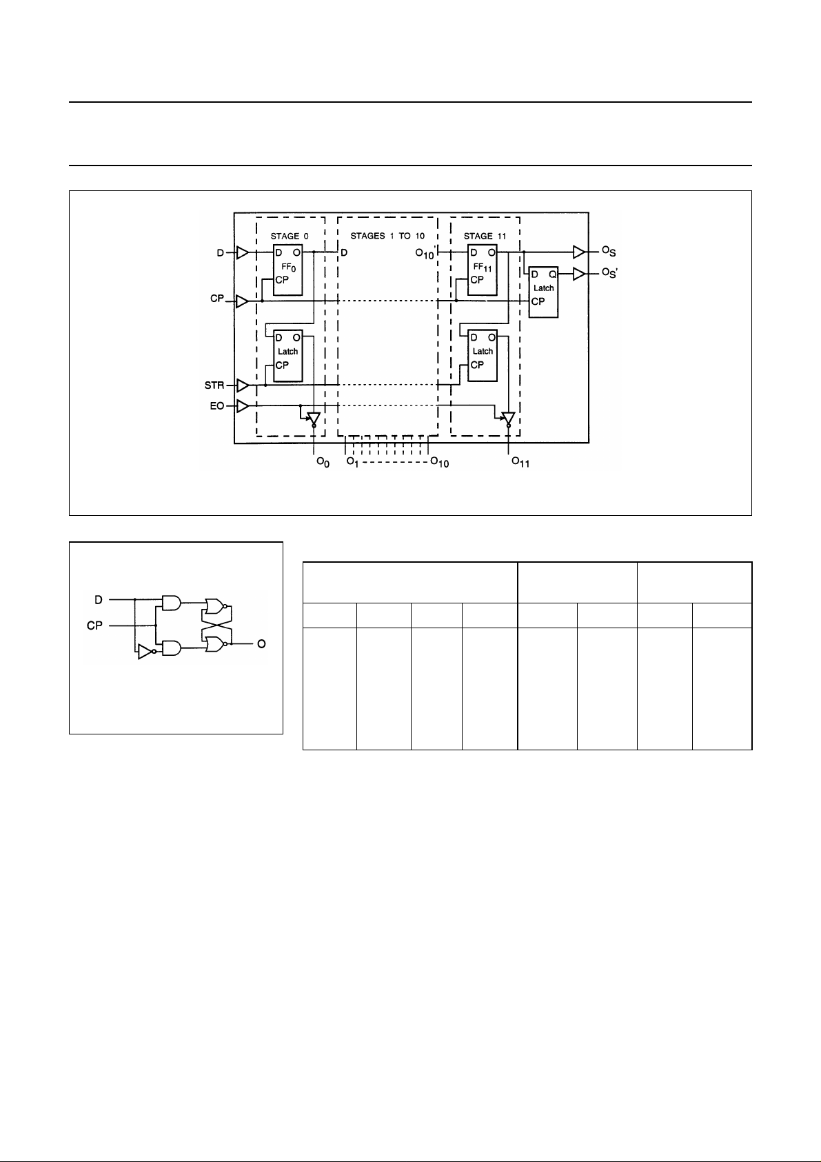
The HEF4894B is a 12 stage serial
shift register having a storage latch
associated with each stage for
strobing data from the serial input to
parallel LED driver outputs O
to
0
O11. Data is shifted on positive-going
clock transitions. The data in each
shift register stage is transferred to
the storage register when the strobe
(STR) input is HIGH. Data in the
storage register appears at the
outputs whenever the output enable
(EO) signal is HIGH.
Two serial outputs (Osand Os’) are
available for cascading a number of
HEF4894B devices. Data is available
at Oson positive-going clock edges to
allow high-speed operation in
cascaded systems in which the clock
rise time is fast. The same serial
information is available at Os’ on the
next negative-going clock edge and
provides cascading HEF4894B
devices when the clock rise time is
slow.
ORDERING AND PACKAGE INFORMATION
TYPE
NUMBER
PINS PIN POSITION MATERIAL CODE
PACKAGES
HEF4894BT 20 SO plastic SO20/SOT163A
HEF4894BP 20 DIL plastic DIL20/SOT146
PINNING
PIN SYMBOL NAME AND FUNCTION
1 STR strobe input
2 D data input
3 CP clock input
4, 5, 6, 7, 8, 9, 18,
O
0
to O
11
parallel outputs (open drain)
17, 16, 15, 14, 13
10 V
11, 12 O
ss
’ serial outputs
s,Os
ground
19 EO output enable input
20 V
DD
positive supply voltage
FAMILY DATA
See Family Specifications except for:
Rating for DC current into any open-drain output: 40 mA.
I
LIMITS category MSI: see Family Specifications.
DD
Preliminary pin assignment.
Fig.1 Pinning diagram.
January 1995 2
Fig.2 Functional diagram.
Page 3
Philips Semiconductors Product specification
12-stage shift-and-store register LED driver HEF4894B
Fig.4 One D-latch.
Fig.3 Logic diagram.
FUNCTION TABLE
INPUTS
CP EO STR D O
PARALLEL
OUTPUTS
0
O
n
↑ LXX Z ZO
SERIAL
OUTPUTS
O
S
’nc
10
↓ LXX Z ZncO
↑ HLXncncO
↑ HHL ZO
↑ HHH LO
−1O10’nc
n
−1O10’nc
n
’nc
10
↓ HHH nc ncncO
Notes
1. H = HIGH state (the more positive voltage)
2. L = LOW state (the less positive voltage)
3. X = state is immaterial
4. ↑ = positive-going transition
5. ↓ = negative-going transition
6. Z = high impedance OFF state
7. nc = no change
8. O
’ = the information in the twelfth shift register stage.
11
OS’
11
11
At the positive clock edge the information in the 10thregister stage is
transferred to the 11thregister stage and the Osoutput.
January 1995 3
Page 4

Philips Semiconductors Product specification
12-stage shift-and-store register LED driver HEF4894B
DC CHARACTERISTICS
V
=0 V.
SS
T
(°C)
amb
V
PARAMETER
output voltage 5 V
LOW; O
n
output leakage 5 I
current; HIGH; O
AC CHARACTERISTICS
V
SS
= 0 V; T
=25°C; input transition times ≤ 20 ns.
amb
DD
(V)
SYMBOL
UNIT CONDITIONS−40 + 25 + 85
MIN. MAX. MIN. MAX. MIN. MAX.
OL
− 0.75 − 0.75 − 1.5 V VI=VSSor VDD;
10 − 0.75 − 0.75 − 1.5 Io < 20 mA
15 − 0.75 − 0.75 − 1.5
OZH
10 − 2 − 2 − 15
n
− 2 − 2 − 15 µAV
15 − 2 − 2 − 15
= 15 V
o
V
PARAMETER
DD
(V)
Dynamic power 5 1200 f
dissipation per package 10 5550 f
(P) 15 15000 f
TYPICAL FORMULA FOR P
(µW)
+∑(foCL) × V
i
+∑(foCL) × V
i
+∑(foCL) × V
i
DD
DD
DD
2
2
2
where:
R
= ∞
load
fi= input frequency (MHz),
= output frequency (MHz),
f
o
C
= load capacitance (pF),
L
) = sum of outputs
∑(f
oCL
V
= supply voltage (V)
DD
AC CHARACTERISTICS
V
= 0 V; T
SS
PARAMETER
=25°C; CL= 50 pF; input transition times ≤ 20 ns.
amb
V
DD
(V)
SYMBOL TYP. MAX. UNIT
TYPICAL EXTRAPOLATION
FORMULA
Propagation delay 5 160 320 132 ns + (0.55 ns/pF) C
CP to O
s
10 t
PHL
65 130 ns 53 ns + (0.23 ns/pF) C
HIGH to LOW 15 45 90 37 ns + (0.16 ns/pF) C
Propagation delay 5 130 260 102 ns + (0.55 ns/pF) C
CP to O
s
10 t
PLH
55 110 ns 44 ns + (0.23 ns/pF) C
LOW to HIGH 15 40 80 32 ns + (0.16 ns/pF) C
Propagation delay 5 120 240 92 ns + (0.55 ns/pF) C
CP to Os’10t
PHL
50 100 ns 39 ns + (0.23 ns/pF) C
HIGH to LOW 15 40 80 32 ns + (0.16 ns/pF) C
Propagation delay 5 130 260 102 ns + (0.55 ns/pF) C
CP to Os’10t
PLH
60 120 ns 49 ns + (0.23 ns/pF) C
LOW to HIGH 15 45 90 37 ns + (0.16 ns/pF) C
L
L
L
L
L
L
L
L
L
L
L
L
January 1995 4
Page 5

Philips Semiconductors Product specification
12-stage shift-and-store register LED driver HEF4894B
PARAMETER
V
(V)
DD
SYMBOL TYP. MAX. UNIT
TYPICAL EXTRAPOLATION
FORMULA
Propagation delay 5 240 480
CP to O
n
10 t
PZL
80 160 ns see note 1
OFF to LOW 15 55 110
Propagation delay 5 170 340
CP to O
n
10 t
PLZ
75 150 ns see note 1
LOW to OFF 15 60 120
Propagation delay 5 140 280
STR to O
n
10 t
PZL
70 140 ns see note 1
OFF to LOW 15 55 110
Propagation delay 5 100 200
STR to O
n
10 t
PLZ
40 100 ns see note 1
LOW to OFF 15 35 70
Output transition 5 85 170 35 ns + (1.0 ns/pF) C
time; Os,Os’10t
THL
40 80 ns 19 ns + (0.42 ns/pF) C
HIGH to LOW 15 30 60 16 ns + (0.28 ns/pF) C
Output transition 5 85 170 35 ns + (1.0 ns/pF) C
time; Os,Os’10t
TLH
40 80 ns 19 ns + (0.42 ns/pF) C
LOW to HIGH 15 30 60 16 ns + (0.28 ns/pF) C
Note
1. Definition of symbol equivalent to 3-state outputs.
L
L
L
L
L
L
AC CHARACTERISTICS
= 0 V; T
V
SS
output enable time 5 t
EO to O
n
=25°C; CL= 50 pF; input transition times ≤ 20 ns.
amb
V
PARAMETER
DD
(V)
SYMBOL MIN. TYP. MAX. UNIT
PZL
10 − 55 110
− 100 200 ns
OFF to LOW 15 − 50 100
output disable time 5 t
EO to O
n
10 − 40 80
PLZ
− 80 160 ns
LOW to OFF 15 − 30 60
minimum clock pulse width 5 t
WCPL
60 30 − ns
LOW 10 30 15 −
15 24 12 −
minimum strobe pulse width 5 t
WSTRH
80 40 − ns
HIGH 10 60 30 −
15 24 12 −
January 1995 5
Page 6

Philips Semiconductors Product specification
12-stage shift-and-store register LED driver HEF4894B
V
PARAMETER
set-up time 5 t
D to CP 10 20 10 −
hold time 5 t
D to CP 10 20 5 −
Maximum clock pulse frequency 5 f
DD
(V)
SYMBOL MIN. TYP. MAX. UNIT
su
60 30 − ns
15 15 5 −
hold
5 −15 − ns
15 20 5 −
max
510 −MHz
10 11 22 −
15 14 28 −
Fig.5 Timing diagram.
January 1995 6
Page 7

Philips Semiconductors Product specification
12-stage shift-and-store register LED driver HEF4894B
APPLICATION INFORMATION
An example of applications for the HEF4894B is:
• Serial-to-parallel converting LED driver
Fig.6 LED driver register.
January 1995 7
 Loading...