

Page 1
INTEGRATED CIRCUITS
DATA SH EET
For a complete data sheet, please also download:
•The IC04 LOCMOS HE4000B Logic
Family Specifications HEF, HEC
•The IC04 LOCMOS HE4000B Logic
Package Outlines/Information HEF, HEC
HEF4738V
LSI
IEC/IEEE bus interface
Product specification
File under Integrated Circuits, IC04
January 1995
Page 2
Philips Semiconductors Product specification
IEC/IEEE bus interface
DESCRIPTION
The HEF4738V is an implementation of the IEC-bus as
described in IEC report 66 CO 22 (interface system for
programmable measuring apparatus) as well as in IEEE
standard 488-1975 (standard digital interface for
programmable instrumentation).
Together with bus-drivers, level converters and
multiplexers it is suitable for connecting electronic
programmable and non-programmable equipment to an
IEC/IEEE interface bus.
All inputs have standard HE4000B family levels.
In the circuit the following standard interface functions are
incorporated:
HEF4738V
LSI
• Complete source handshake (subset SH1)
• Complete acceptor handshake (subset AH1)
• Basic talker with serial poll and talk-only mode (when It
= LOW, subset T1; It = HIGH, subset T5)
• Basic listener with listen-only mode (when It = LOW,
subset L1; It = HIGH, subset L3)
• Complete service request (subset SR1)
• Complete remote local (subset RL1)
• Remote parallel poll configuration (subset PP1)
• Complete device clear (subset DC1)
• Complete device trigger (subset DT1)
• Some controller facilities
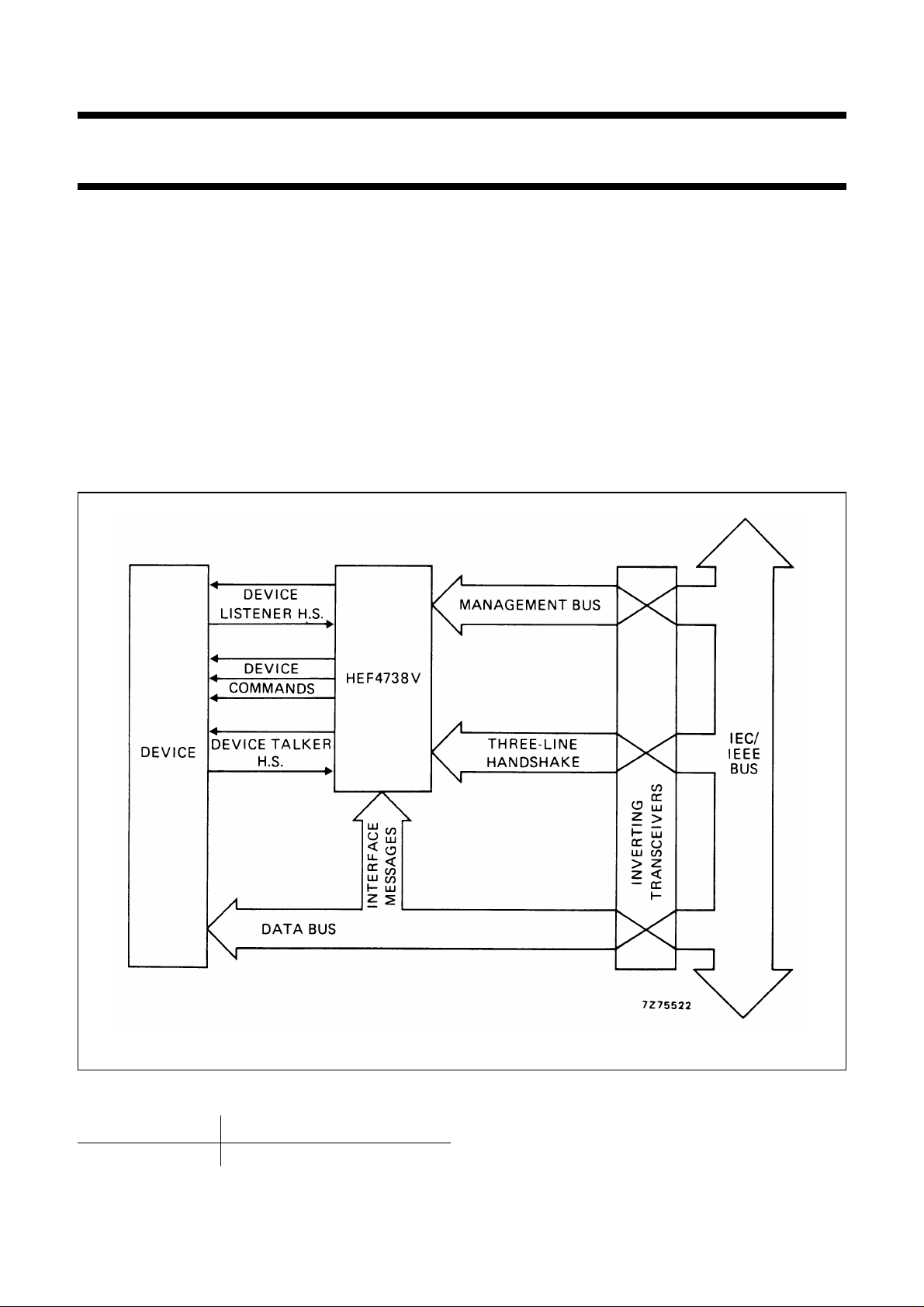
Fig.1 Basic IEC/IEEE bus interface using the HEF4738V.
SUPPLY VOLTAGE
RATING RECOMMENDED OPERATING
−0,5 to 18 4,5 to 12,5 V
January 1995 2
FAMILY DATA, IDDLIMITS category LSI
See Family Specifications
Page 3

Philips Semiconductors Product specification
IEC/IEEE bus interface
GENERAL DESCRIPTION
The inputs IRFD, IDAC,IDAV,IIFC, IREN, IATN, IIDY and
IDIO1 to IDIO7 must be connected via an inverting TTL to
LOCMOS level converter to the respective bus lines:
NRFD, NDAC, DAV, IFC, REN, ATN, IDY and DIO1 to
DIO7.
The outputs ORFD, ODAC, ODAV and OSRQ can drive
one standard TTL load and are suitable for driving NRFD,
NDAC, DAV and SRQ via an inverting bus-driver circuit.
The parallel poll outputs OP1, OP2, OP3 and OPP can
also drive one standard TTL load. Outputs OP1, OP2 and
OP3 are connected to flip-flops, which store the attendant
bits P1, P2 and P3 of the last PPE message. OP1, OP2
and OP3 have to be decoded externally and multiplexed to
the DIO-lines when OPP is LOW.
All other output stages are standard HE4000B family.
Most of the functions in the IEC/IEEE interface IC are
realized with synchronous sequential logic, which is driven
from the clock input CP. HIGH to LOW transitions are used
to synchronize input signals and LOW to HIGH transitions
trigger the internal flip-flops. In order to meet the IEC/IEEE
timing specifications, the maximum clock frequency is
2 MHz. The maximum data transfer is then
200 kbytes/second.
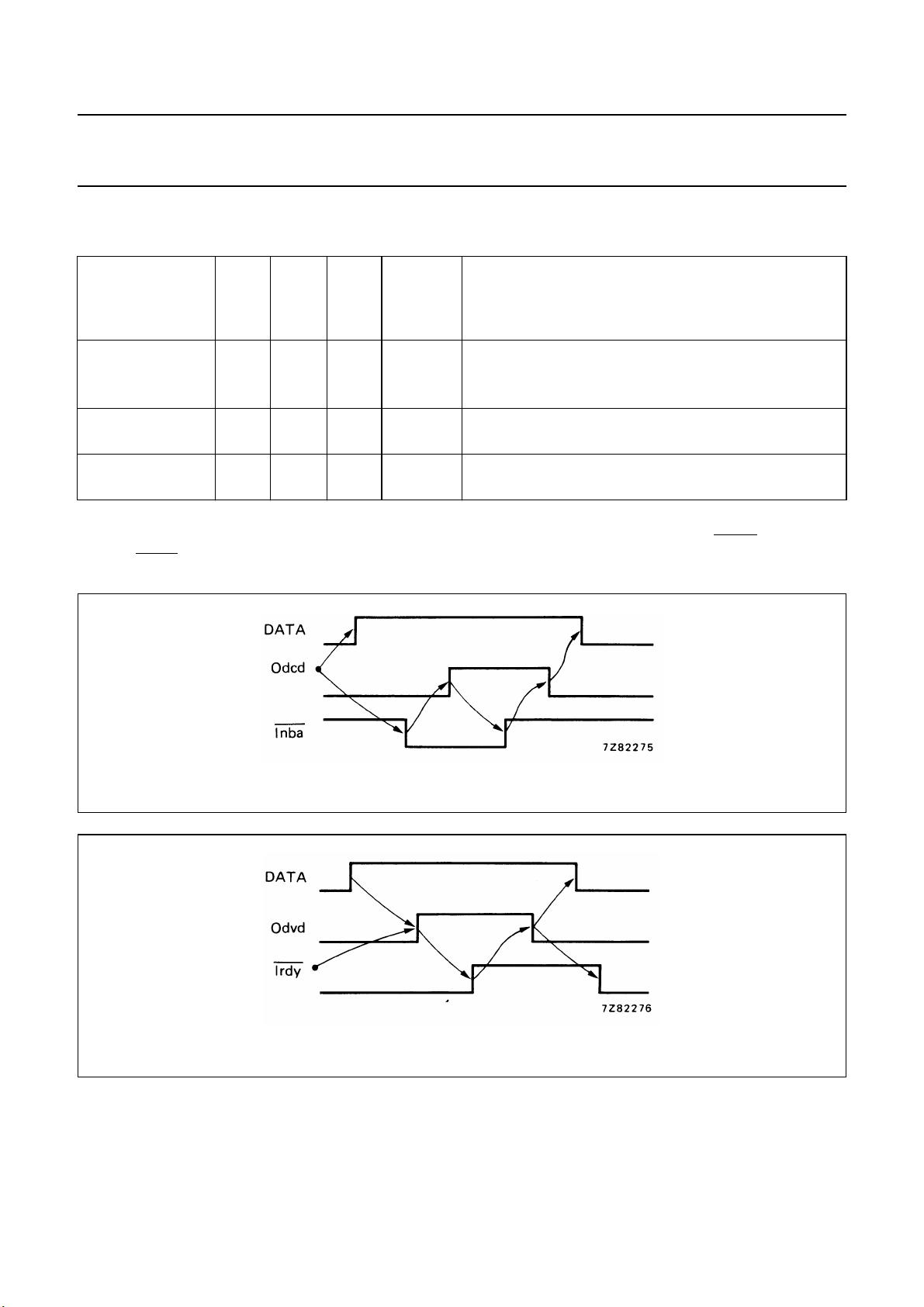
Irdy (not ready for next message) and output Odvd
Input
(data valid device) are intended for a two-wire handshake
procedure between the acceptor function in the IC and the
data input of the device (instrument to be connected to the
interface system). The procedure is made so, that if the
device reacts fast enough, the handshake procedure can
be omitted by interconnecting Odvd and Irdy. The
conditions to be fulfilled by the device are:
• The device must be able to accept a data byte within one
clock period after dvd goes HIGH under all conditions.
• The device must be ready to process a data byte within
two clock periods plus the minimum settling time of the
talker devices under all conditions.
Input Inba (not new byte available) and output Odcd (don’t
change data) are intended for a two-wire handshake
procedure with the source function in the IC and the data
output of the device (instrument). The procedure is so
made that if the device reacts fast enough the handshake
procedure can be omitted by interconnecting Odcd and
Inba. The conditions to be fulfilled by the device are:
• The device must be able to set a new data byte on the
bus within one clock period after dcd goes LOW under
all conditions.
• The device must be able to have the next data byte
available within seven clock periods under all
conditions.
HEF4738V
LSI
Input Isr and output Ored should be connected to an
external parallel-in/serial-out (when Ored is HIGH
parallel-in, when LOW serial-out) shift register, which must
be connected to the clock CP and must trigger on the LOW
to HIGH transitions. The data on the parallel inputs of this
external shift register are loaded in parallel and shifted-out
via input Isr into an internal shift register. The eleven serial
input signals are in the order of shifting: A5, A4, A3, A2,
A1, ton, Ion, It, rsv, rtl and ist.
Signals A5, A4, A3, A2 and A1 represent the device talker
and listener address. When signal It (either listener or
talker) is HIGH, a listener addressing sets the talker to the
idle state and a talker addressing sets the listener to the
idle state (subset T5 and L3). With It LOW, the device can
be addressed to be a listener and a talker. Because of the
serial input procedure, all these input signals arrive in the
interface functions of the IC between 16 and 32 clock
cycles.
The signals ton, Ion, rsv, rtl and ist are standard IEC/IEEE
inputs. When using ton or Ion no controller action is
possible.
The output Oclr or Otrg is HIGH for one clock pulse if
DCAS (device clear active state) or DTAS (device trigger
active state) respectively is active.
The output Oloc is HIGH when LOCS (local state) or LWLS
(local with lock-out state) is active. Output
when the rsv signal is read from the external shift register
and the SRQS (request service state) is active. After this
request has been answered by a serial poll, ORQS is
HIGH in the APRS (affirmative poll response state). The
inverted signal on ORQS must be multiplexed to bus-line
DIO7, together with the status byte of the other DIO lines,
when output Osp is HIGH in the SPAS (serial poll active
state).
When the device is in the SPAS state the signal rsv may
be removed (can be checked on ORQS). N.B.: When the
interface has asked for service via rsv and is addressed as
talker in the serial poll mode, a handshake must be
initialized by the device via Inba.
Input Icats and output Otct are intended for use of this IC
in a controller. When Icats is HIGH, the source handshake
function will exit SIDS and SIWS and enter respectively
SGNS and SWNS. When the controller function is not
used, the input Icats must be connected to VSS. Output
Otct is HIGH if the tct message is sent over the interface
and the ACDS state is active. A HIGH on input Ipon sets
each function to its initial state. This level can be set to
LOW after the IC has received 32 clock pulses at stabilized
supply voltage.
OSRQ is HIGH
January 1995 3
Page 4
Philips Semiconductors Product specification
IEC/IEEE bus interface
Note
After power-on the input Ipon must stay LOW for at least
32 clock pulses, then HIGH for 32 clock pulses in order to
force the function to its initial state.
After this, Ipon must be set LOW.
HEF4738V
Input pins
1,2,3,36,
37, 38, 39
4 =
IIDY input IDY not
9 = Isr (note 1) input shift register
11 =
IIFC input IFC not
12 = Ipon input pon
IDAV input DAV not
13 =
14 = Irdy input rdy not
18 =
IATN input ATN not
24 = IRFD input RFD
25 = Inba input nba not
26 = IDAC input DAC
27 = lcats inputs cats
28 =
IREN input REN not
31 = CP clock pulse input
= ID101 to 7: input DIO
LSI
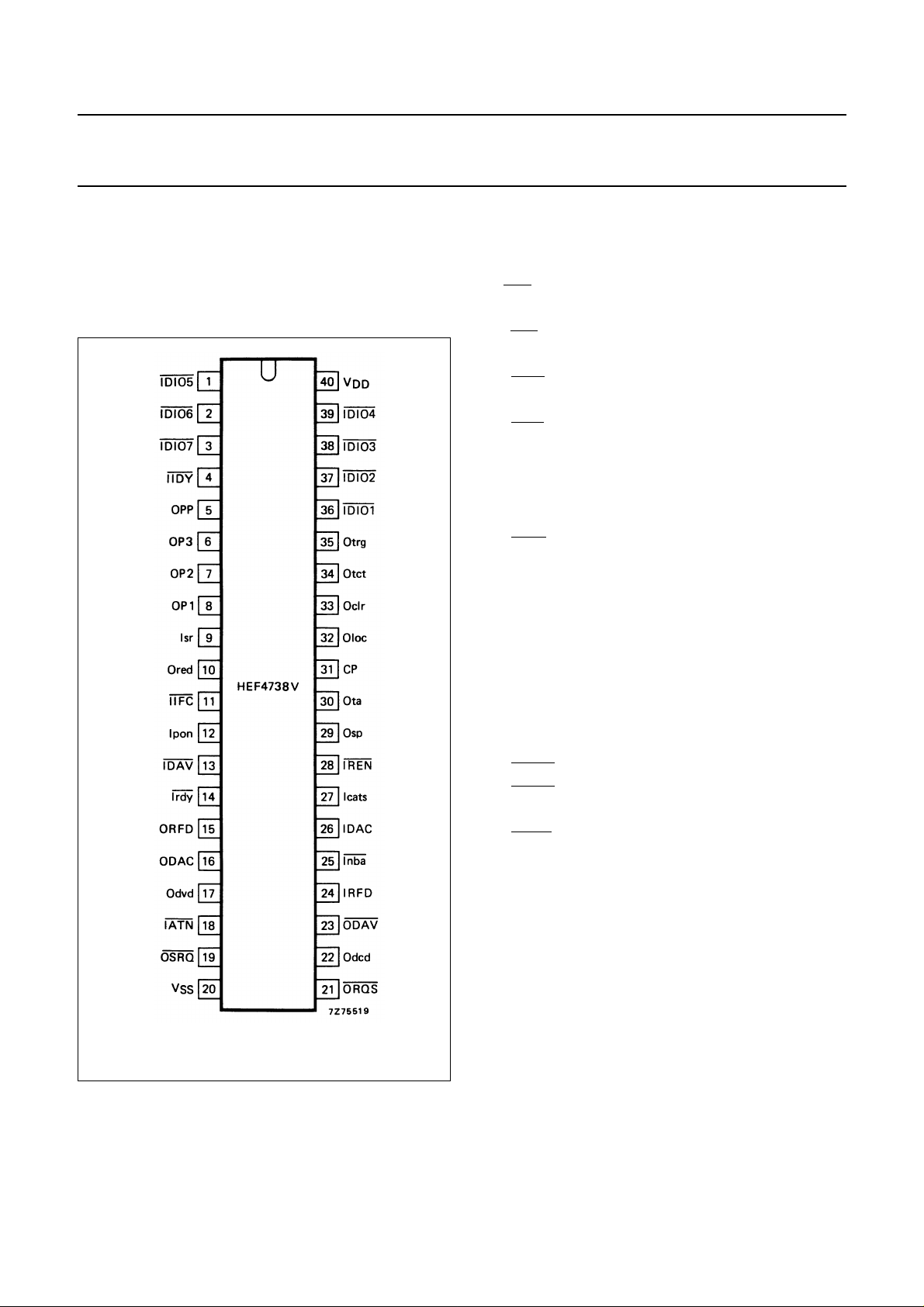
Fig.2 Pinning diagram; for abbreviations see the
following list.
Output pins
5 = OPP output PP
8,7,6, = OP1 to OP3 output P1 to P3
10 = Ored output red
15 = ORFD output RFD
16 = ODAC output DAC
17 = Odvd output dvd
19 =
OSRQ output SRQ not
21 =
ORQS output RQS not
22 = Odcd output dcd
23 =
ODAV output DAV not
29 = Osp output sp
30 = Ota output ta
32 = Oloc output loc
33 = Oclr output clr
34 = Otct output tct
35 = Otrg output trg
Supply pins
20 = V
40 = V
: more negative supply line
SS
: more positive supply line
DD
HEF4738VP(N): 40-lead DIL; plastic (SOT129-1)
( ): Package Designator North America
January 1995 4
Note
1. Isr is serial input for signals A5, A4, A3, A2, A1, ton,
Ion, lt, rsv, rtl and ist.
Page 5
January 1995 5
Note
Because the circuit uses positive logic and the bus uses negative logic,
all inputs and outputs to the bus must be inverted. For that reason, all
terminals that are working with the bus have mnemonics which are the
inverted ones of those on the bus.
Philips Semiconductors Product specification
IEC/IEEE bus interface
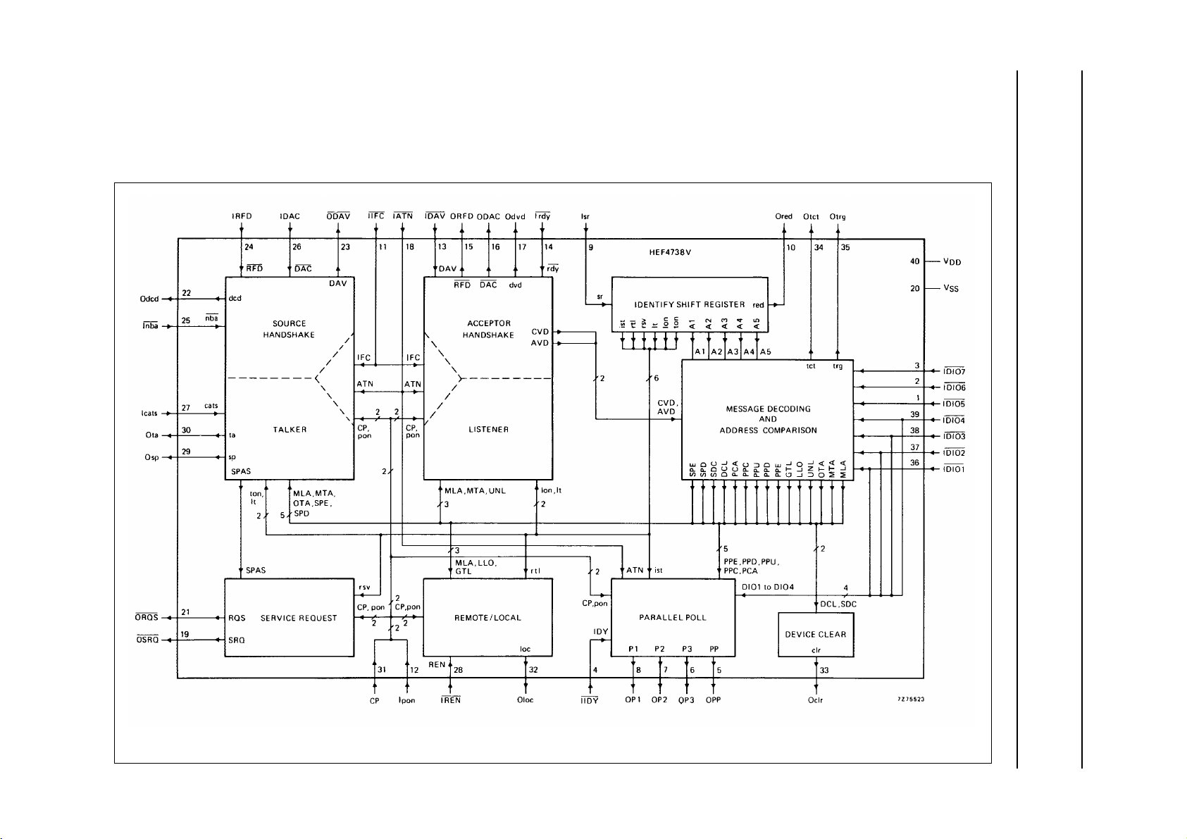
Fig.3 Block diagram.
HEF4738V
LSI
Page 6

Philips Semiconductors Product specification
IEC/IEEE bus interface
LIST OF USED ABBREVIATIONS
A1 to A5 address
ACDS acceptor data state
APRS affirmative poll response state
ATN attention
AVD address valid
cats controller active or transfer state
clr device clear
CVD command valid
DAC data accepted
DAV data valid
DCAS device clear active state
dcd don’t change data
DCL device clear
DIO data input output
DTAS device trigger active state
dvd data valid device
EOI end of output/identify
GTL go to local
IDY identify
IFC interface clear
ist individual status
LLO local lock-out
loc local
LOCS local state
Ion listen only
It decides whether the device can only be
listener/talker or listener and talker
simultaneously
LWLS local with lock-out state
MLA my listen address
MTA my talk address
nba new byte available
NRFD not ready for data
NDAC not data accepted
OTA other talk address
P1 to P3 parallel response messages
PCA parallel poll configure accepted
pon power on
PP parallel poll message enable
PPC parallel poll configure
PPD parallel poll disable
HEF4738V
LSI
PPE parallel poll enable
PPU parallel poll unconfigure
rdy ready for next message
red ready for next shift cycle
REN remote enable
RFD ready for data
RQS requested service
rsv request for service
rtl return to local
SDC selected device clear
SGNS source generate state
SIDS source idle state
SIWS source idle wait state
sp serial poll
SPAS serial poll active state
SPD serial poll disable
SPE serial poll enable
sr shift register
SRQ service request
SRQS request service state
SWNS source wait for new cycle state
ta talker active
tct talk control
ton talk only
trg trigger
UNL unlisten
January 1995 6
Page 7
Philips Semiconductors Product specification
IEC/IEEE bus interface
HEF4738V
DC CHARACTERISTICS
V
=0 V
SS
T
(°C)
amb
V
V
Output current 5 2,5 3 2,5 2,0 mA
HIGH; see note 5 4,6 −I
Output current 4,75 0,4
LOW; see note 10 0,5 9,5 8,0 6,3 mA
Quiscent device 5 50 50 375 µA
current 10 I
Note
1. Output currents for pins: 5 = OPP, 6 = OP3, 7 = OP2, 8 = OP1, 15 = ORFD, 16 = ODAC; 19 =
23 = ODAV. These pins can drive one standard TTL load.
DD
V
V
OL
V
OH
V
SYMBOL
−40 + 25 + 85
MIN. MAX. MIN. MAX. MIN. MAX.
OH
1 0,85 0,65 mA
10 9,5 3 2,5 2,0 mA
I
OL
DD
2,7 2,3 1,8 mA
100 100 750 µA
OSRQ,
LSI
Fig.4 Waveforms showing data exchange in talker function.
Fig.5 Waveforms showing data exchange in listener function.
January 1995 7
Page 8
Philips Semiconductors Product specification
IEC/IEEE bus interface
APPLICATION INFORMATION
HEF4738V
LSI
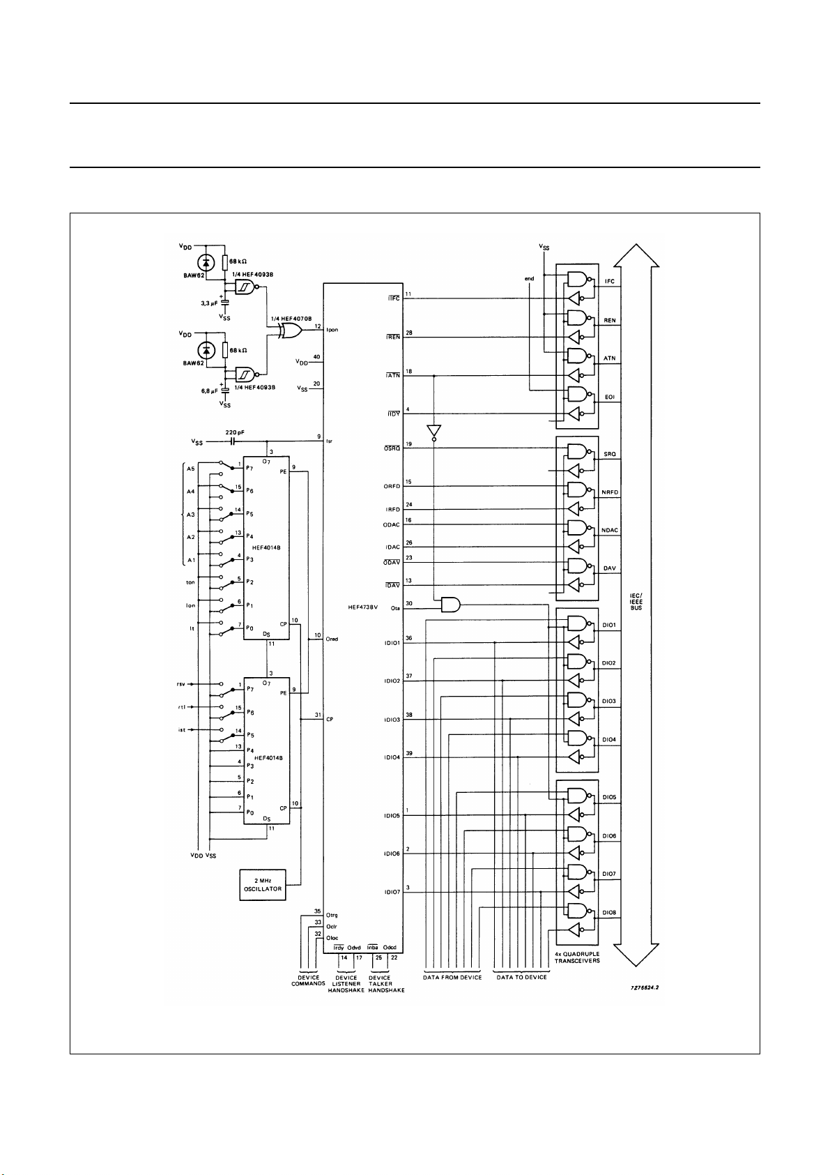
Fig.6 Basic listener and talker. Serial and parallel poll are not implemented.
January 1995 8
 Loading...