

Page 1
INTEGRATED CIRCUITS
DATA SH EET
For a complete data sheet, please also download:
•The IC04 LOCMOS HE4000B Logic
Family Specifications HEF, HEC
•The IC04 LOCMOS HE4000B Logic
Package Outlines/Information HEF, HEC
HEF4720B
HEF4720V
LSI
256-bit, 1-bit per word random
access memories
Product specification
File under Integrated Circuits, IC04
January 1995
Page 2
Philips Semiconductors Product specification
HEF4720B
256-bit, 1-bit per word random access memories
HEF4720V
DESCRIPTION
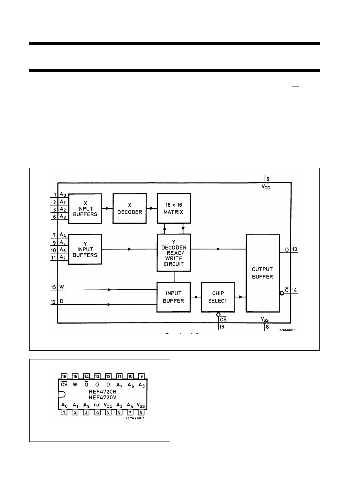
The HEF4720B and HEF4720V are 256-bit, 1-bit per word
random access memories with 3-state outputs. The
memories are fully decoded and completely static.
Recommended supply voltage range for HEF4720B is 3 to
15 V and for HEF4720V is 4,5 to 12,5 V; minimum
stand-by voltage for both types is 3 V.
The use of LOCMOS gives the added advantage of very
low stand-by power. The circuits can be directly interfaced
with standard bipolar devices (TTL) without using special
interface circuits. The memory operates from a single
power supply. The separate chip select input (
simple memory expansion when the outputs are wire-O
Red. If CS is HIGH, the outputs are floating and no new
information can be written into the memory. The signal at
O has the same polarity as the data input D, while the
signal at O is the complement of the signal at O. The write
control W must be HIGH for writing into the memory.
CS) allows
Fig.1 Functional diagram.
Fig.2 Pinning diagram.
January 1995 2
HEF4720BP; HEF4720VP(N): 16-lead DIL; plastic
(SOT38-1)
HEF4720BD; HEF4720VD(F): 16-lead DIL; ceramic
(cerdip) (SOT74)
HEF4720BT; HEF4720VT(D): 16-lead SO; plastic
(SOT109-1)
( ): Package Designator North America
FAMILY DATA
See Family Specifications.
Page 3
Philips Semiconductors Product specification
HEF4720B
256-bit, 1-bit per word random access memories
IDDLIMITS
See below.
HEF4720V
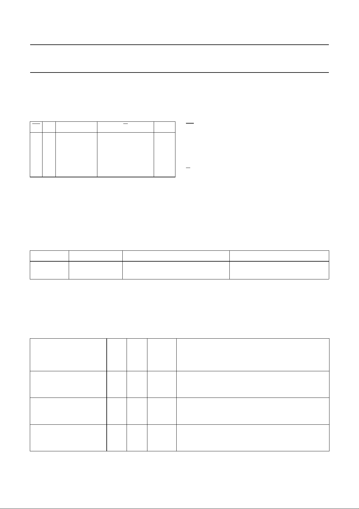
FUNCTION TABLE
CS W O O MODE
L H data written complement of data write
into memory written into memory
L L data written complement of data read
into memory written into memory
H X Z Z inhibit
PINNING
CS chip select input (active LOW)
W write enable input
D data input
A
0
to A
7
address inputs
O 3-state output (active HIGH)
O 3-state output (active LOW)
Notes
1. H = HIGH state (the more positive voltage)
L = LOW state (the less positive voltage)
X = state is immaterial
Z = high impedance OFF-state
SUPPLY VOLTAGE
RATING RECOMMENDED OPERATING STAND-BY MIN.
HEF4720B −0,5 to 18 3,0 to 15,0 3 V
HEF4720V −0,5 to 18 4,5 to 12,5 3 V
The values given at VDD= 15 V in the following DC and
AC characteristics, are not applicable to the HEF4720V,
because of its lower supply voltage range.
DC CHARACTERISTICS
=0 V
V
SS
T
(°C)
amb
V
V
DD
V
OL
V
SYMBOL
−40 +25 +85
MIN. MAX. MIN. MAX. MIN. MAX.
Output current 4,75 0,4 2,4 2 1,6 mA
LOW 10 0,5 I
OL
4,8 4 3,2 mA
15 1,5 10,0 10 7,5 mA
Quiescent device 5 25 25 200 µA
current 10 I
DD
50 50 400 µA
15 100 100 800 µA
Input leakage current
HEF4720V 10
HEF4720B 15 0,3 0,3 1 µA
±I
IN
0,3 0,3 1 µA
January 1995 3
Page 4
Philips Semiconductors Product specification
HEF4720B
256-bit, 1-bit per word random access memories
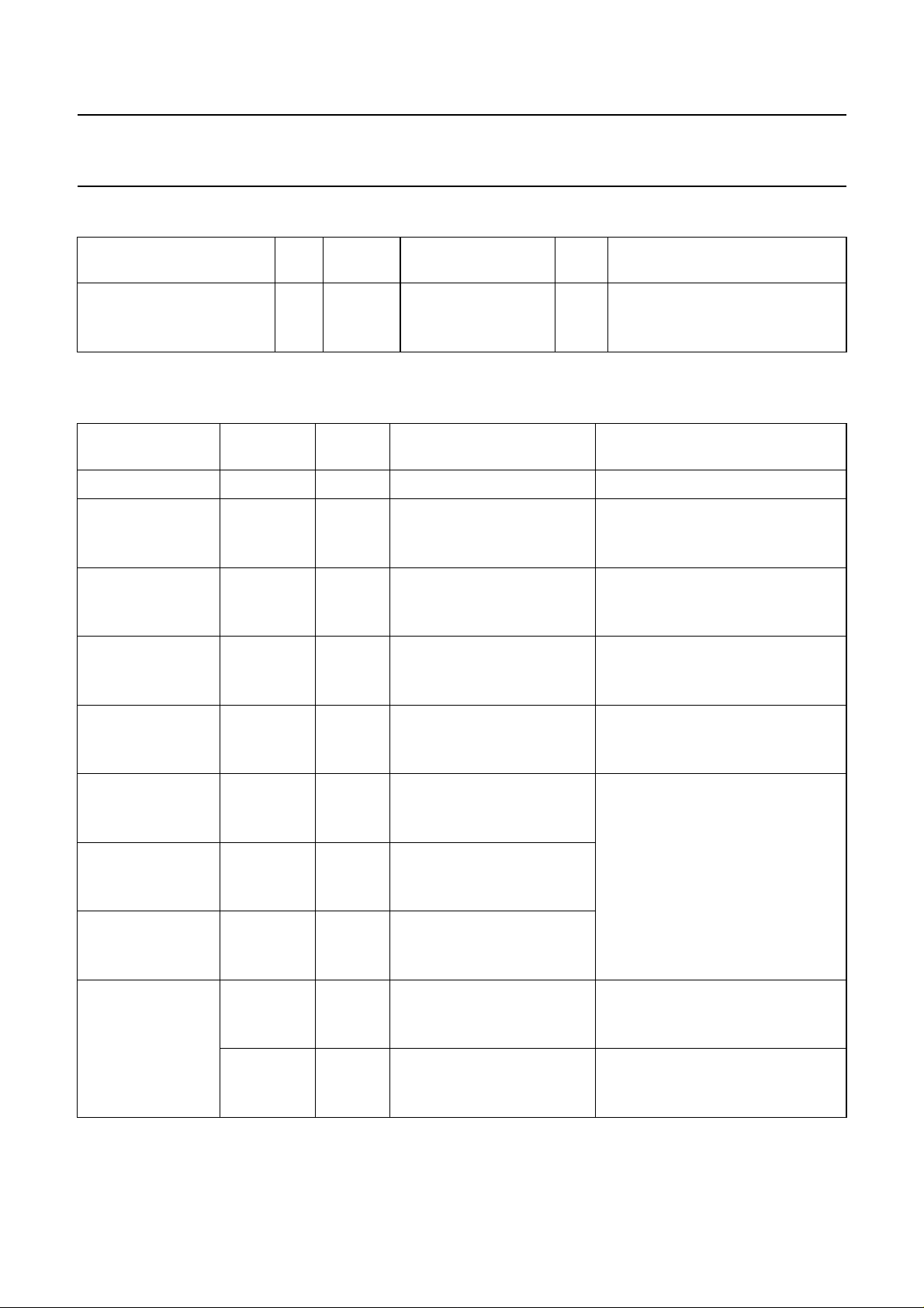
AC CHARACTERISTICS
V
DD
SYMBOL MIN. TYP. MAX.
V
55pF
Output capacitance 10 C
15 5 pF
A.C. CHARACTERISTICS
V
SS
= 0 V; T
=25°C; CL= 50 pF; input transition times ≤ 20 ns
amb
O
5pF
HEF4720V
V
DD
V
SYMBOL MIN. TYP. MAX.
TYPICAL EXTRAPOLATION
FORMULA
Read cycle
5 320 580 ns 292 ns + (0,55 ns/pF) C
Read access time 10 t
ACC
130 220 ns 118 ns + (0,23 ns/pF) C
15 100 160 ns 92 ns + (0,16 ns/pF) C
Chip select to 5 180 ns
output time 10 t
CO
70 ns
15 50 ns
50ns
Address hold time 10 t
OA
0ns
15 0 ns
Output hold time 5 60 170 ns 142 ns + (0,55 ns/pF) C
with respect to 10 t
VAL1
20 50 ns 38 ns + (0,23 ns/pF) C
address input 15 15 40 ns 32 ns + (0,16 ns/pF) C
Output hold time 5 130 ns
with respect to 10 t
COH
70 ns
chip select input 15 60 ns
Output floating time 5 0 ns
with respect to 10 t
COF
0ns
chip select input 15 0 ns
5 580 ns
Read cycle time 10 t
RC
220 ns
15 160 ns
Output transition 5 60 120 ns 10 ns + (1,0 ns/pF) C
times 10 t
TLH
30 60 ns 9 ns + (0,42 ns/pF) C
LOW to HIGH 15 20 40 ns 6 ns + (0,28 ns/pF) C
54080ns14ns+(0,52 ns/pF) C
HIGH to LOW 10 t
THL
22 40 ns 11 ns + (0,22 ns/pF) C
15 15 30 ns 7 ns + (0,16 ns/pF) C
L
L
L
L
L
L
L
L
L
L
L
L
January 1995 4
Page 5

Philips Semiconductors Product specification
HEF4720B
256-bit, 1-bit per word random access memories
AC CHARACTERISTICS
V
= 0 V; T
SS
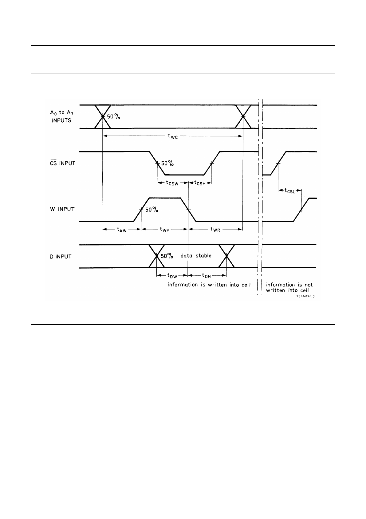
Write cycle
Write cycle time 10 t
Address to write 5 110 ns
set-up time 10 t
Write pulse width 10 t
Write recovery time 10 t
Data set-up time 10 t
Data hold time 10 t
Chip select set-up 5 370 ns
time with respect 10 t
to write pulse 15 80 ns
Chip select hold 5 0 ns
time with respect 10 t
to write pulse 15 0 ns
Chip select lead time 5 0 ns
over write pulse to 10 t
prevent writing 15 0 ns
=25°C; CL= 50 pF; input transition times ≤ 20 ns
amb
V
DD
V
SYMBOL MIN. TYP. MAX.
5 580 ns
WC
220 ns
15 160 ns
AW
15 50 ns
5 370 10 000 ns
WP
130 10 000 ns
15 80 10 000 ns
5 100 ns
WR
15 30 ns
5 250 ns
DW
100 ns
15 80 ns
5 100 ns
DH
15 20 ns
CSW
CSH
CSL
130 ns
50 ns
40 ns
30 ns
0ns
0ns
HEF4720V
January 1995 5
Page 6
Philips Semiconductors Product specification
HEF4720B
256-bit, 1-bit per word random access memories
V
DD
V
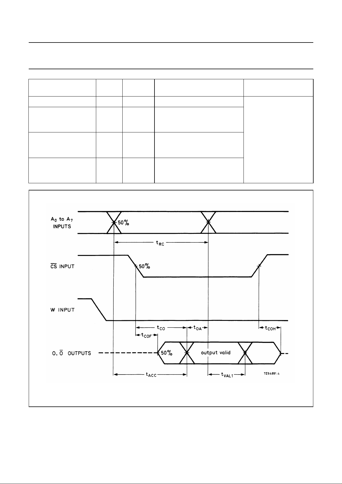
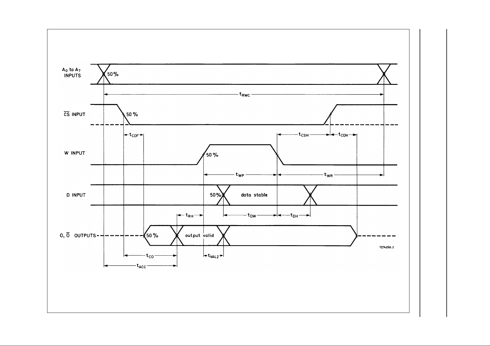
Read-modify-write cycle
Read enable 5 0 ns
hold time 10 t
15 0 ns
Output hold time 5 60 ns
with respect to 10 t
write pulse 15 15 ns
Read-modify-write 5 1050 ns
cycle time 10 t
15 270 ns
SYMBOL MIN. TYP. MAX.
RH
VAL2
RWC
0ns
20 ns
390 ns
HEF4720V
Fig.3 Read cycle timing diagram.
January 1995 6
Page 7
Philips Semiconductors Product specification
HEF4720B
256-bit, 1-bit per word random access memories
HEF4720V
Fig.4 Write cycle timing diagram.
January 1995 7
Page 8
This text is here in white to force landscape pages to be rotated correctly when browsing through the pdf in the Acrobat reader.This text is here in
_white to force landscape pages to be rotated correctly when browsing through the pdf in the Acrobat reader.This text is here inThis text is here in
white to force landscape pages to be rotated correctly when browsing through the pdf in the Acrobat reader. white to force landscape pages to be ...
January 1995 8
Philips Semiconductors Product specification
256-bit, 1-bit per word random access
memories
Fig.5 Read-modify-write cycle timing diagram.
HEF4720B
HEF4720V
Page 9

Philips Semiconductors Product specification
HEF4720B
256-bit, 1-bit per word random access memories
APPLICATION INFORMATION
Extension of memory capacity
The memory capacity of the HEF4720B; V is 256 bits (or
256 words of 1 bit). The capacity of a system can be
extended in various ways by the connection of further
HEF4720B; V ICs.
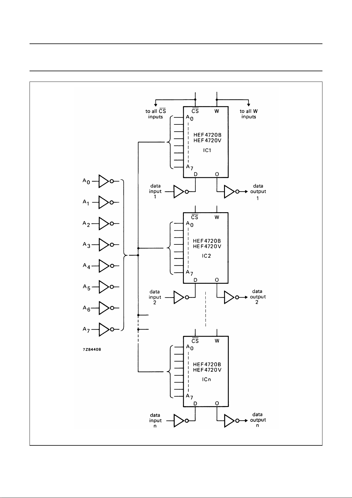
Extending the word length
By connecting a number of HEF4720B; V ICs as shown in
Fig.6, the word length (i.e. bits per word) is multiplied by
that number. That is, each device stores 1 bit per word but
the total number of words remains 256. For example, if
four devices are used in this way, 256 four-binary-bit words
can be stored.
Extending the number of words
HEF4720V
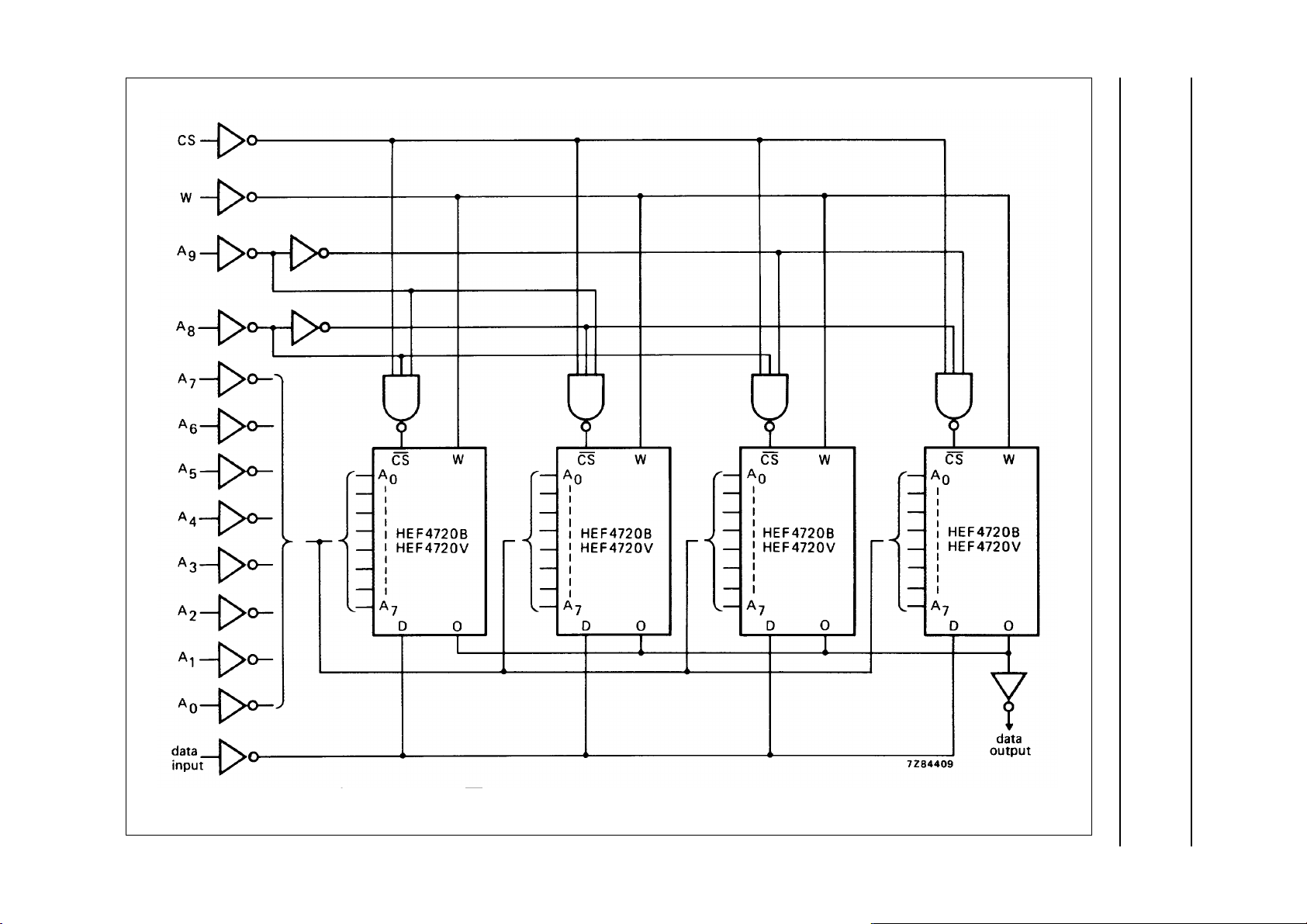
If a number of HEF4720B; V ICs are connected as shown
in Fig.7, the words available are multiplied by that number,
but the word length remains 1 bit. Notice that in this case
additional addresses are used in conjunction with the
CS input. In the case shown in Fig.7 (4 × HEF4720B; V in
parallel), the addresses and data inputs are loaded with
four inputs (= 20 pF), the CS inputs are loaded with one
input each.
Extending both the word length and number of words
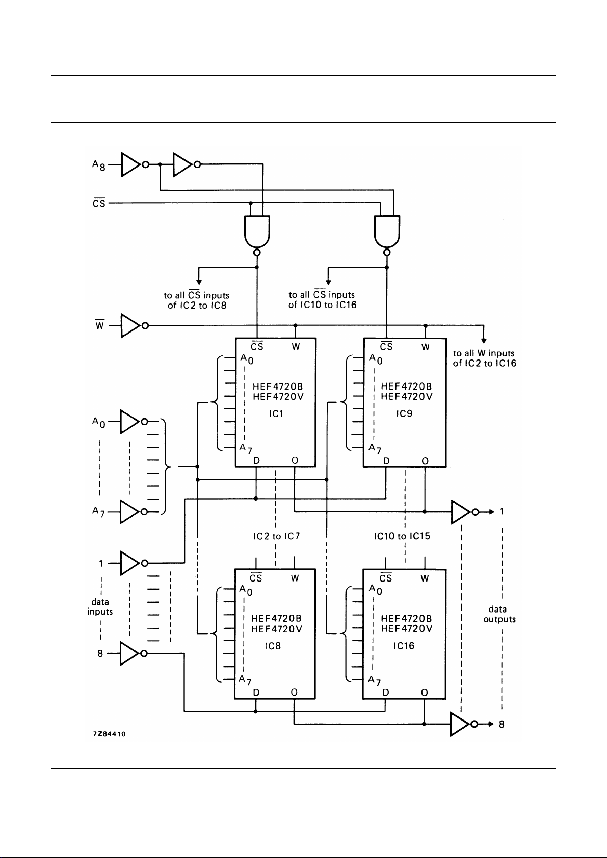
Figure 8 shows how a combination of the extensions
described above can be used to obtain both greater word
length and additional words. It is clear that the capacitive
load of the driving circuits puts a limit to the free choice of
the interface. In Fig.8, each address is loaded with 16
inputs, i.e. 16 × 5 = 80 pF: each CS inverter is loaded with
8 inputs, i.e. 8 × 5 = 40 pF. The data inverters in this case
are loaded with only two inputs each.
January 1995 9
Page 10
Philips Semiconductors Product specification
HEF4720B
256-bit, 1-bit per word random access memories
HEF4720V
Fig.6 Using extra HEF4720B; V ICs to extend the word length.
January 1995 10
Page 11
This text is here in white to force landscape pages to be rotated correctly when browsing through the pdf in the Acrobat reader.This text is here in
_white to force landscape pages to be rotated correctly when browsing through the pdf in the Acrobat reader.This text is here inThis text is here in
white to force landscape pages to be rotated correctly when browsing through the pdf in the Acrobat reader. white to force landscape pages to be ...
January 1995 11
Philips Semiconductors Product specification
256-bit, 1-bit per word random access
memories
Fig.7 Using extra HEF4720B; V ICs to obtain more words.
HEF4720B
HEF4720V
Page 12
Philips Semiconductors Product specification
HEF4720B
256-bit, 1-bit per word random access memories
HEF4720V
Fig.8 Using extra HEF4720B; V ICs to obtain more words and greater word length.
January 1995 12
Page 13

Philips Semiconductors Product specification
HEF4720B
256-bit, 1-bit per word random access memories
HEF4720V
Memory retention
It is sometimes necessary to ensure that the information
stored in the memory cannot be erased inadvertently. This
can be arranged by adding detection circuits, by measures
in the timing, and by the addition of a battery. With the
HEF4720B; V, memory retention is very easily obtained
because its current drain in the stand-by condition is
almost zero. The wide supply voltage range makes it
possible to keep the memory active by means of a simple
battery, thereby preventing information loss.
In designing the memory retention circuits, two aspects
should be kept in mind. The memory retention will not
function in an optimum way if the battery voltage is low or
if the voltage transitions at the address input are too slow.
The first of these is usually the result of using too simple a
battery back-up circuit, e.g. a battery charged via a diode
from the TTL supply voltage. In this case, the LOCMOS
supply voltage falls below the safe operating voltage.
Special arrangements should be made to overcome this.
Slow address transitions (the second cause of memory
loss) are due to a long RC-time in the power system. When
the power is switched on or off, the 5 V line changes
between 0 and 5 V in milliseconds to seconds so
producing a correspondingly long transition time in the
various logic outputs. This creates problems in the proper
operation of the HEF4720B; V, with loss of memory as a
possible result. This can be prevented by ensuring that
input rise and fall times do not exceed 10 µs.
Three possibilities for controlling the rise and fall times at
the HEF4720B; V interface are given here:
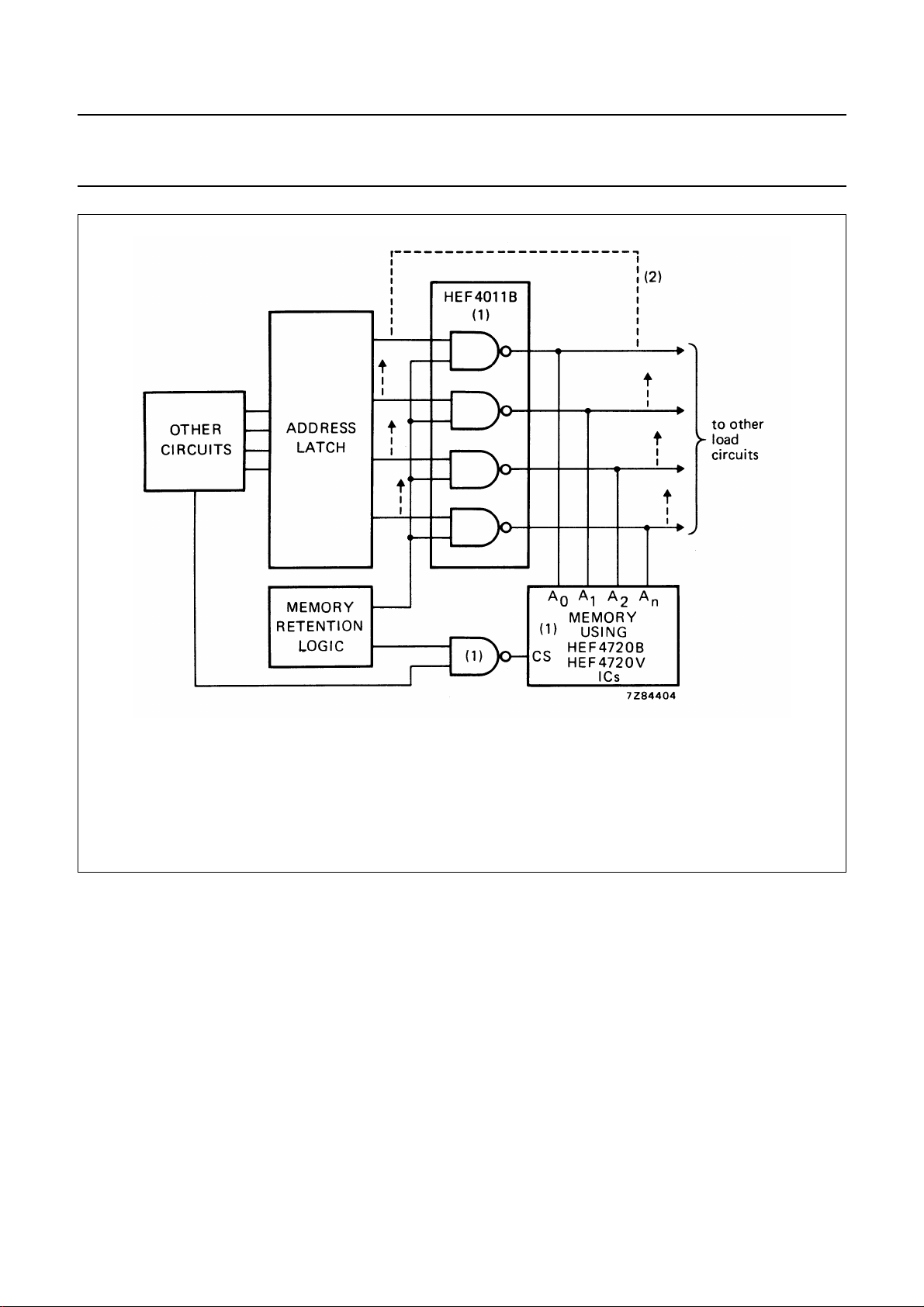
1. LOCMOS gates can be connected between the
address latch and the HEF4720B; V (Fig.9). In the
event of a low voltage, or mains supply failure, the
gates can be blocked by a signal from the memory
retention logic thus isolating the HEF4720B; V from
the address and
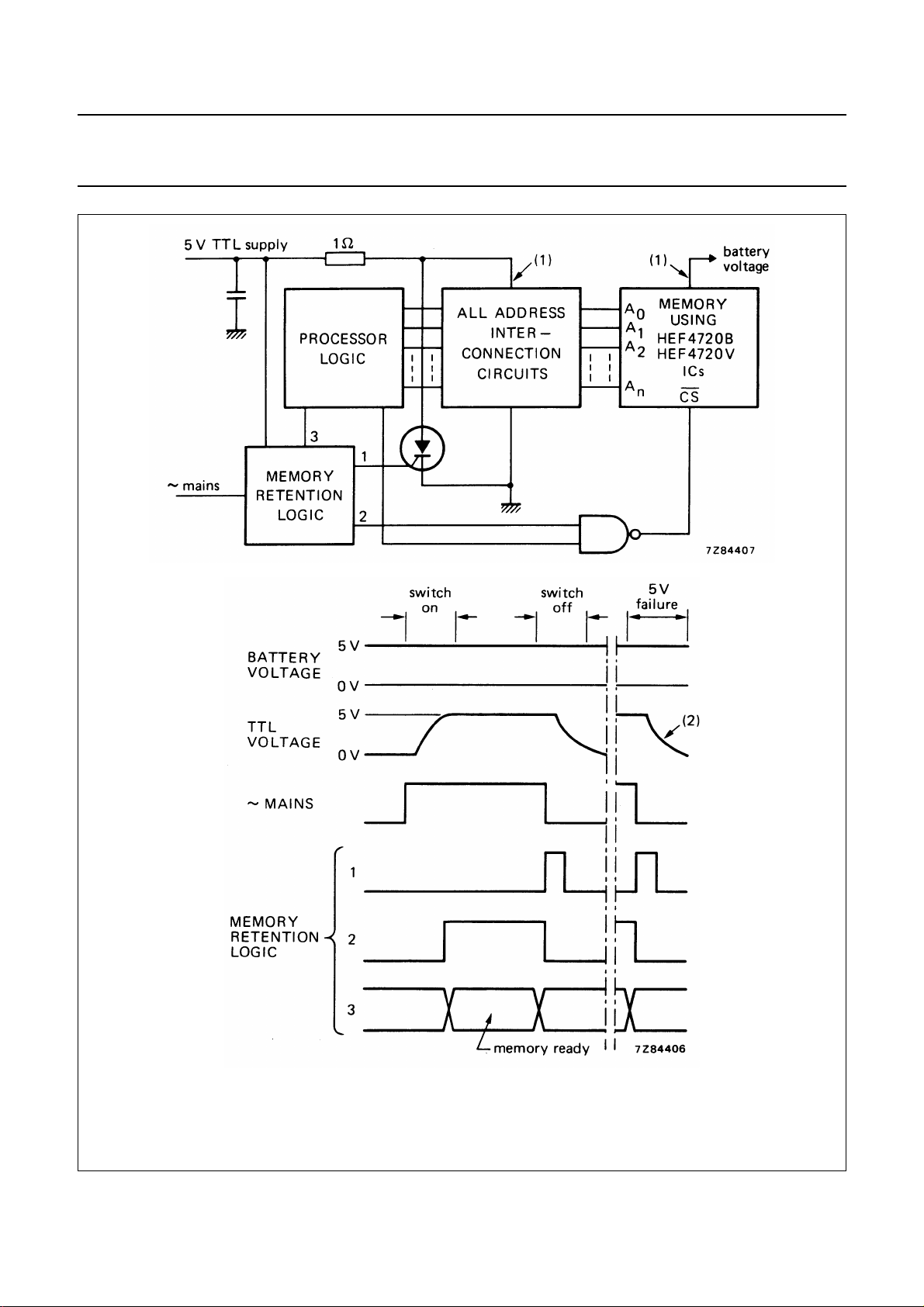
2. The interface power supply can be separated from the
TTL power supply by means of a low-value resistor
(Fig.10); a thyristor is connected from the interface
power supply to earth. The system is arranged so that,
upon switching off or failure of the interface supply, the
thyristor turns on thus ensuring a rapid fall of the
supply voltage.
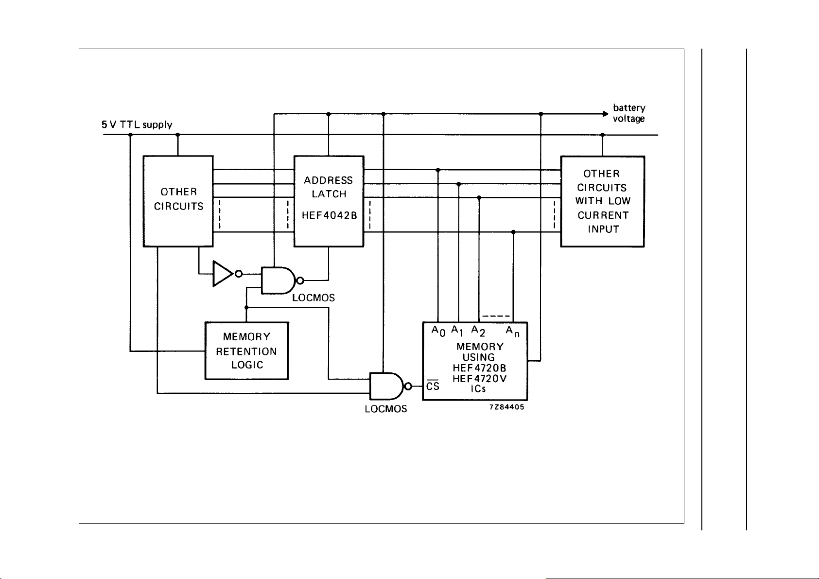
3. The best solution is to select the interface circuits from
the LOCMOS family and to feed all these circuits from
the battery (Fig.11). These stages then remain active
when the TTL 5 V supply fails. The interface circuits
are mostly only active on a clock pulse, have the
possibility of being inactive on a gate level, or can be
forced into one position.
CS inputs.
January 1995 13
Page 14
Philips Semiconductors Product specification
HEF4720B
256-bit, 1-bit per word random access memories
HEF4720V
(1) These devices have a battery supply.
(2) Alternative connection.
Fig.9 Use of battery-operated LOCMOS gates to isolate the memory in case of power supply failure. Devices
marked (1) are connected to the battery. The HEF4011B can sink about 0,7 mA: if the load is greater than
this, only the memory should be connected, other loads being connected to the address latch as shown
by the dashed-line connections.
January 1995 14
Page 15
Philips Semiconductors Product specification
HEF4720B
256-bit, 1-bit per word random access memories
HEF4720V
(1) Leads should be so arranged to prevent cross-talk; thyristor connections must be short.
(2) Slope > 500 mV/µs in the vicinity of the threshold.
Fig.10 Using a thyristor to ensure a rapid fall of interface supply at switch-off or supply failure.
January 1995 15
Page 16
This text is here in white to force landscape pages to be rotated correctly when browsing through the pdf in the Acrobat reader.This text is here in
_white to force landscape pages to be rotated correctly when browsing through the pdf in the Acrobat reader.This text is here inThis text is here in
white to force landscape pages to be rotated correctly when browsing through the pdf in the Acrobat reader. white to force landscape pages to be ...
January 1995 16
Philips Semiconductors Product specification
256-bit, 1-bit per word random access
memories
Fig.11 Preferred solution for memory retention; all interface circuits are battery-fed LOCMOS. Note that maximum sink current of the
HEF4042B is about 1,5 mA.
HEF4720B
HEF4720V
 Loading...