

Page 1

INTEGRATED CIRCUITS
DATA SH EET
For a complete data sheet, please also download:
•The IC04 LOCMOS HE4000B Logic
Family Specifications HEF, HEC
•The IC04 LOCMOS HE4000B Logic
Package Outlines/Information HEF, HEC
HEF4527B
MSI
BCD rate multiplier
Product specification
File under Integrated Circuits, IC04
January 1995
Page 2
Philips Semiconductors Product specification
BCD rate multiplier
DESCRIPTION
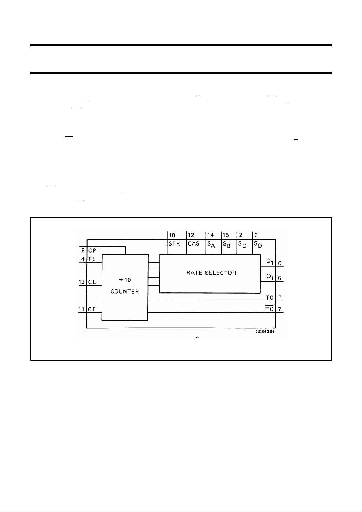
The HEF4527B is a BCD rate multiplier with two buffered
rate outputs (O1 and O1), two buffered terminal count
outputs (TC and TC), four BCD rate select inputs (SA, SB,
SC, SD), a common clock input (CP), a preset input (PL),
an overriding asynchronous clear input (CL), a strobe input
(STR), a cascade input (CAS) and an active LOW count
enable input (CE).
The BCD rate multiplier provides an output pulse rate
based upon the BCD input number. For example, if 6 is the
BCD number, there will be six output pulses for every ten
clock input pulses. The output is clocked on the
negative-going transition of the clock.
CE, STR, CAS, CL and PL are LOW, the rate pulses
When
are available at the outputs O1 and O1, the terminal count
pulses at TC and TC.
HEF4527B
MSI
A HIGH on CL resets the counter, independent of all other
input conditions and a rate of 10 pulses is available at O
and O1when SDis HIGH. When CE is HIGH, the counter
is disabled, the state of the outputs (O1, O1) depend on the
content of the counter.
A HIGH on PL sets the counter in the ‘9’ state and TC
becomes HIGH.
A HIGH on STR inhibits the outputs O1and O1. A HIGH on
CAS forces the output O1to HIGH, while the state of
O1depends on the inputs SAto SD(see lines 1 to 16 of
function table).
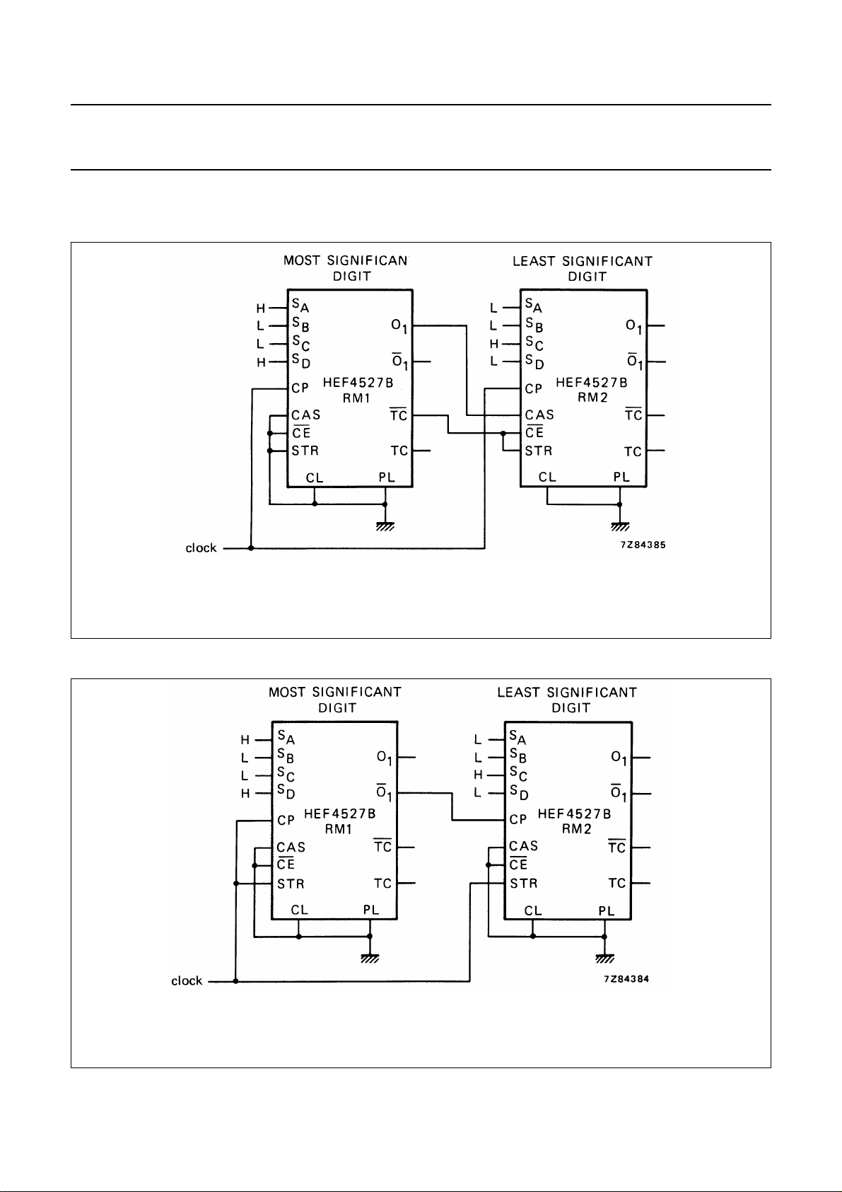
This device may be used to perform arithmetic operations.
For the add mode and multiply mode see Figs 5 and 6.
Schmitt-trigger action in the clock input makes the circuit
highly tolerant to slower clock rise and fall times.
1
Fig.1 Functional diagram.
FAMILY DATA, I
See Family Specifications
January 1995 2
LIMITS category MSI
DD
Page 3
Philips Semiconductors Product specification
BCD rate multiplier
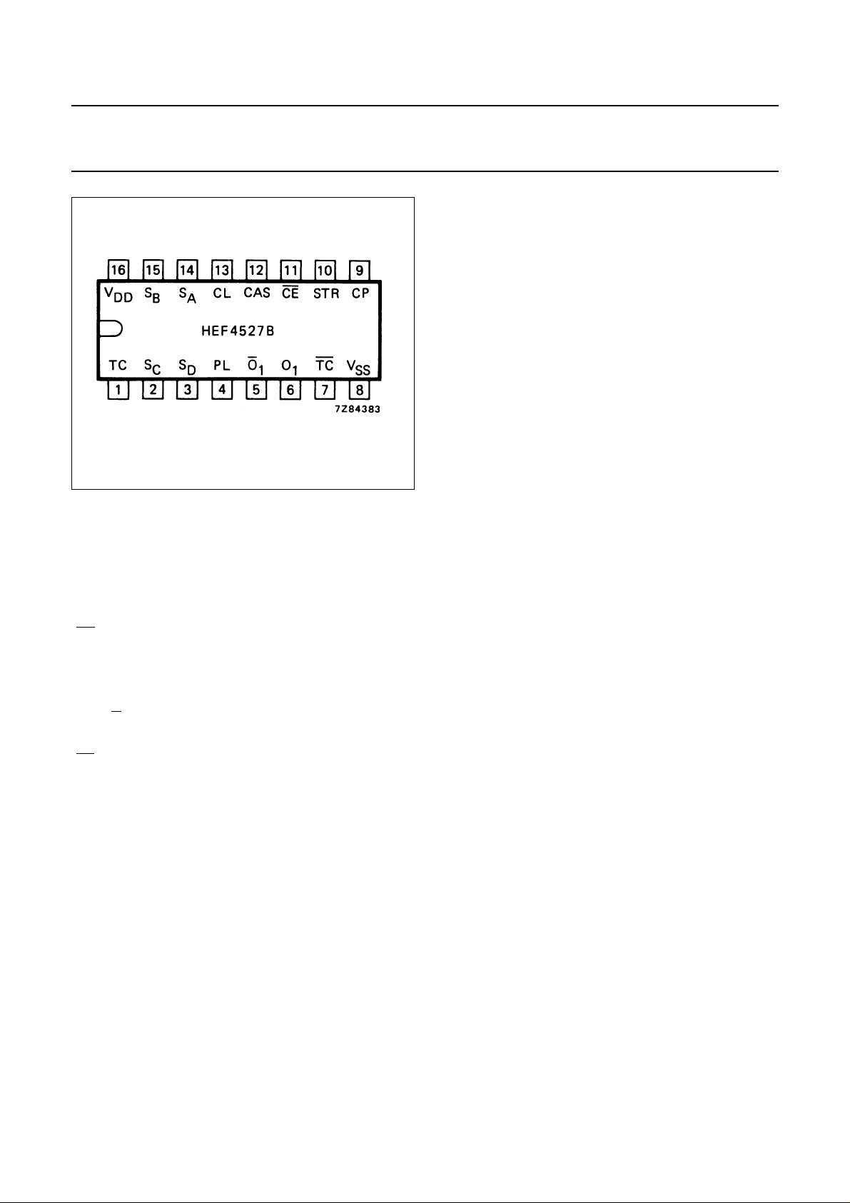
Fig.2 Pinning diagram.
HEF4527B
MSI
HEF4527BP(N): 16-lead DIL; plastic
(SOT38-1)
HEF4527BD(F): 16-lead DIL; ceramic (cerdip)
(SOT74)
HEF4527BT(D): 16-lead SO; plastic
(SOT109-1)
( ): Package Designator North America
PINNING
CP clock input
PL preset to ‘9’ input
CL counter clear input
CE count enable input (active LOW)
STR strobe input
CAS cascade input
S
to S
A
D
O
to O
1
TC terminal count output (active HIGH)
TC terminal count output (active LOW)
rate select inputs
rate outputs
1
January 1995 3
Page 4
This text is here in white to force landscape pages to be rotated correctly when browsing through the pdf in the Acrobat reader.This text is here in
_white to force landscape pages to be rotated correctly when browsing through the pdf in the Acrobat reader.This text is here inThis text is here in
white to force landscape pages to be rotated correctly when browsing through the pdf in the Acrobat reader. white to force landscape pages to be ...
January 1995 4
Philips Semiconductors Product specification
BCD rate multiplier
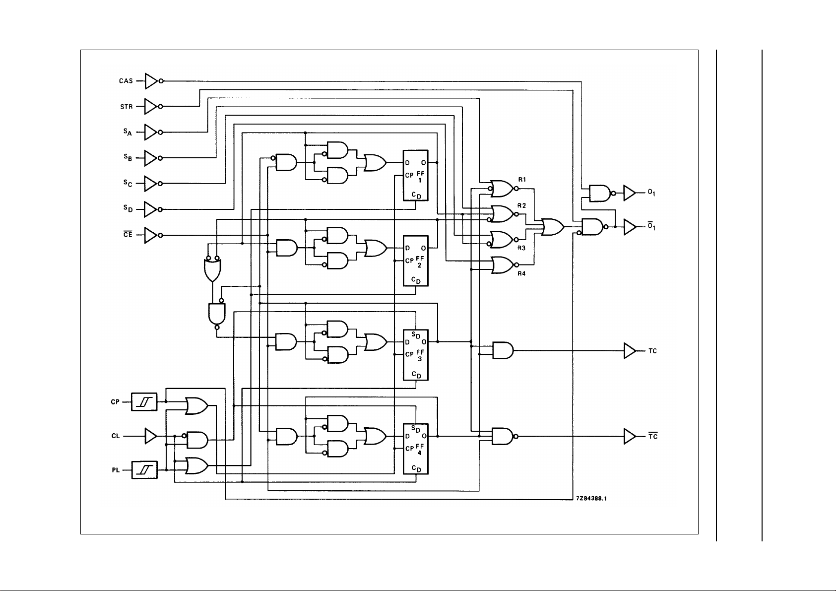
Fig.3 Logic diagram.
HEF4527B
MSI
Page 5
Philips Semiconductors Product specification
BCD rate multiplier
HEF4527B
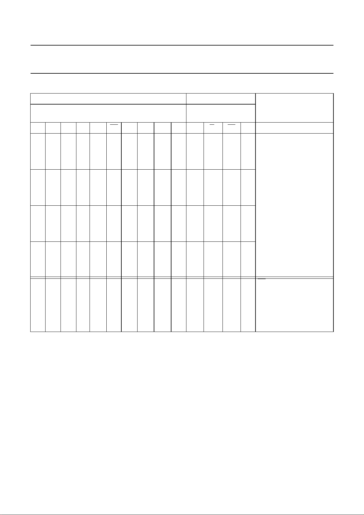
FUNCTION TABLE
INPUTS OUTPUTS
NUMBER OF PULSES OR LOGIC LEVEL NUMBER OF PULSES
OR LOGIC LEVEL
S
DSC
SBSACP CE STR CAS CL PL O
O
1
TC TC
1
L L L L 10 L L L L L L H 1 1
L L L H 10 L L L L L 1 1 1 1
L L H L 10 L L L L L 2 2 1 1
L L H H 10 L L L L L 3 3 1 1
L H L L 10 L L L L L 4 4 1 1
L H L H 10 L L L L L 5 5 1 1
L H H L 10 L L L L L 6 6 1 1
L H H H 10 L L L L L 7 7 1 1
H L L L 10 L L L L L 8 8 1 1
H L L H 10 L L L L L 9 9 1 1
H L H L 10 L L L L L 8 8 1 1
H L H H 10 L L L L L 9 9 1 1
H H L L 10 L L L L L 8 8 1 1
H H L H 10 L L L L L 9 9 1 1
H H H L 10 L L L L L 8 8 1 1
H H H H 10 L L L L L 9 9 1 1
XXXXXHL L L L
(5) (5)
H
X X X X 10 L H L L L L H 1 1 outputs O
XXXX10LL H L L H
(4)
1 1 output O1disabled
H X X X 10 L L L H X 10 10 H L CL = H
L X X X X L L L H X L H H L counter reset
X X X X X L L L L H L H L H PL = H; preset to ‘9’
MODE OF OPERATION
rate pulses at the outputs
depend on the BCD input
number at S
(5)
CE = H; counter disabled
A
and O2disabled
1
to S
MSI
D
Notes
1. H = HIGH state (the more positive voltage)
2. L = LOW state (the less positive voltage)
3. X = state is immaterial
4. Same output as the first 16 lines of this function table (depends on the values of S
5. Depends on internal state of the counter.
January 1995 5
to SD).
A
Page 6
Philips Semiconductors Product specification
BCD rate multiplier
HEF4527B
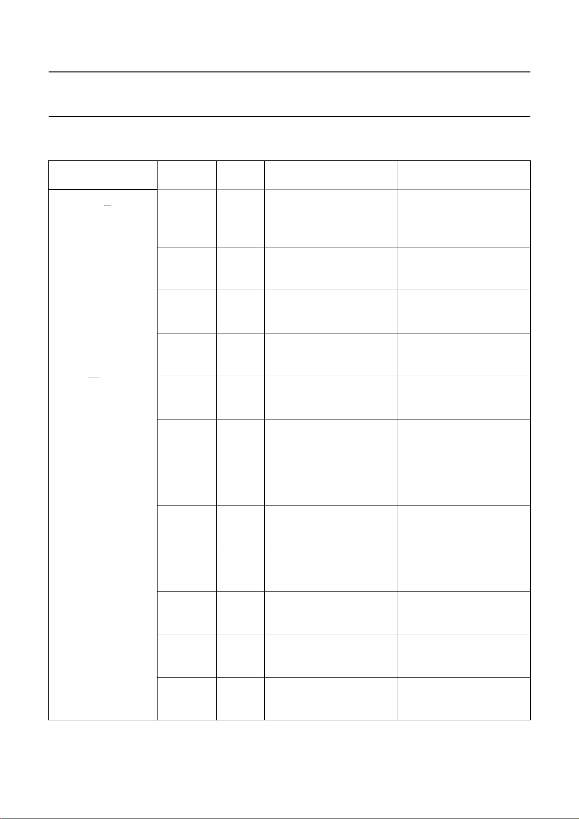
AC CHARACTERISTICS
V
=0V; T
SS
PARAMETER
Propagation delays
CP → O1, O
HIGH to LOW 10 t
LOW to HIGH 10 t
CP → TC 5 175 350 ns 148 ns + (0,55 ns/pF) C
HIGH to LOW 10 t
LOW to HIGH 10 t
CP → TC 5 175 350 ns 148 ns + (0,55 ns/pF) C
HIGH to LOW 10 t
LOW to HIGH 10 t
CAS → O
HIGH to LOW 10 t
LOW to HIGH 10 t
STR → O1, O
HIGH to LOW 10 t
LOW to HIGH 10 t
CE →TC 5 95 190 ns 68 ns + (0,55 ns/pF) C
HIGH to LOW 10 t
LOW to HIGH 10 t
=25°C; CL= 50 pF; input transition times ≤ 20 ns.
amb
V
DD
V
1
5 130 260 ns 103 ns + (0,55 ns/pF) C
SYMBOL MIN. TYP. MAX. UNIT
PHL
15 35 70 ns 27 ns + (0,16 ns/pF) C
5 130 260 ns 103 ns + (0,55 ns/pF) C
PLH
15 35 70 ns 27 ns + (0,16 ns/pF) C
PHL
15 45 90 ns 37 ns + (0,16 ns/pF) C
5 160 320 ns 133 ns + (0,55 ns/pF) C
PLH
15 45 90 ns 37 ns + (0,16 ns/pF) C
PHL
15 50 100 ns 42 ns + (0,16 ns/pF) C
5 150 300 ns 123 ns + (0,55 ns/pF) C
PLH
15 45 90 ns 37 ns + (0,16 ns/pF) C
1
5 90 180 ns 63 ns + (0,55 ns/pF) C
PHL
15 25 50 ns 17 ns + (0,16 ns/pF) C
5 70 140 ns 43 ns + (0,55 ns/pF) C
PLH
15 25 50 ns 17 ns + (0,16 ns/pF) C
1
5 100 200 ns 73 ns + (0,55 ns/pF) C
PHL
15 30 60 ns 22 ns + (0,16 ns/pF) C
5 85 170 ns 58 ns + (0,55 ns/pF) C
PLH
15 25 50 ns 17 ns + (0,16 ns/pF) C
PHL
15 25 50 ns 17 ns + (0,16 ns/pF) C
5 65 130 ns 38 ns + (0,55 ns/pF) C
PLH
15 20 40 ns 12 ns + (0,16 ns/pF) C
TYPICAL EXTRAPOLATION
FORMULA
50 100 ns 39 ns + (0,23 ns/pF) C
50 100 ns 39 ns + (0,23 ns/pF) C
65 130 ns 54 ns + (0,23 ns/pF) C
65 130 ns 54 ns + (0,23 ns/pF) C
65 130 ns 54 ns + (0,23 ns/pF) C
60 120 ns 49 ns + (0,23 ns/pF) C
35 70 ns 24 ns + (0,23 ns/pF) C
30 60 ns 19 ns + (0,23 ns/pF) C
40 80 ns 29 ns + (0,23 ns/pF) C
35 70 ns 24 ns + (0,23 ns/pF) C
35 70 ns 24 ns + (0,23 ns/pF) C
30 60 ns 19 ns + (0,23 ns/pF) C
MSI
L
L
L
L
L
L
L
L
L
L
L
L
L
L
L
L
L
L
L
L
L
L
L
L
L
L
L
L
L
L
L
L
L
L
L
L
January 1995 6
Page 7
Philips Semiconductors Product specification
BCD rate multiplier
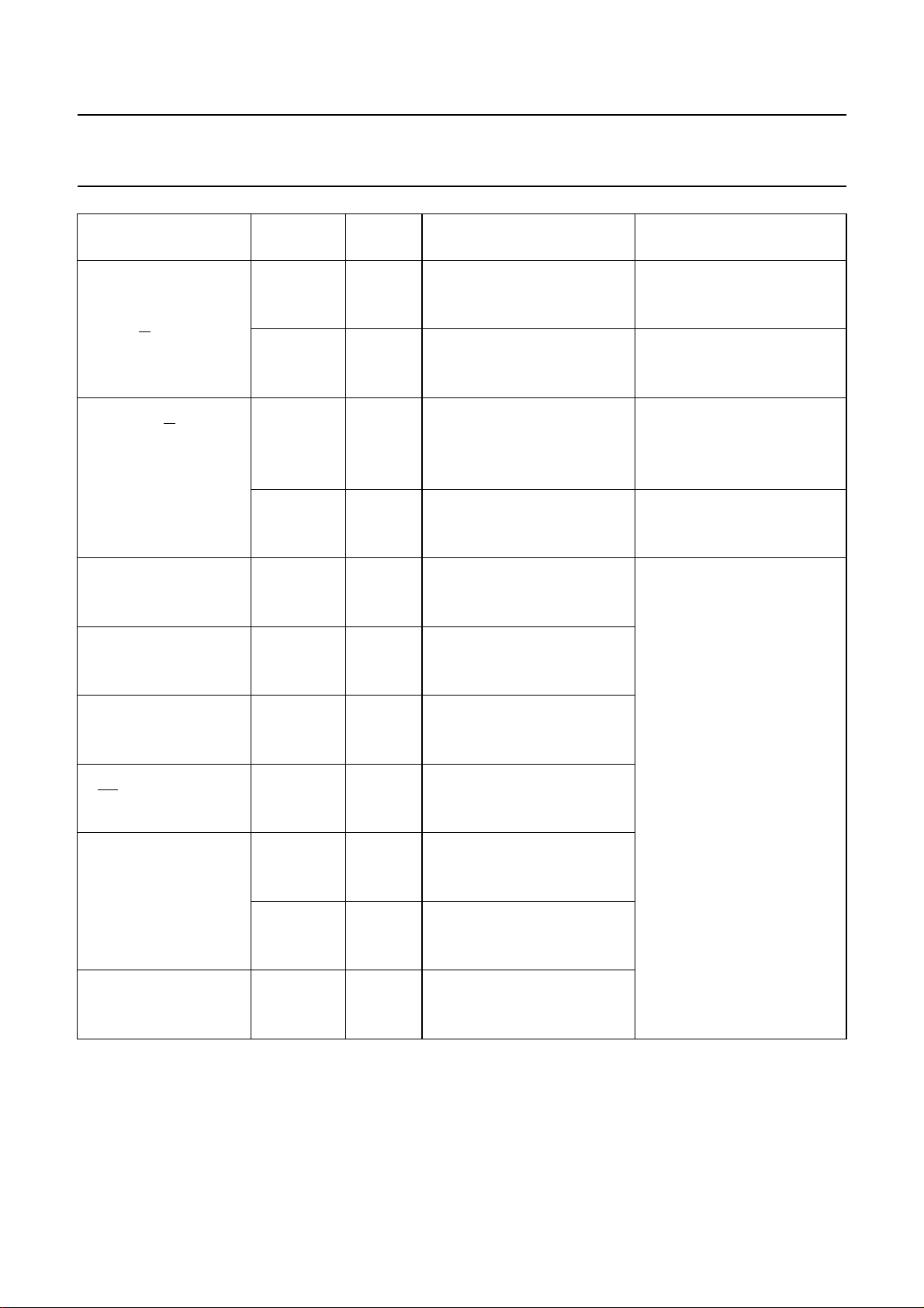
V
PARAMETER
CL → O
1
HIGH to LOW 10 t
CL → O
1
LOW to HIGH 10 t
Propagation delays
PL → O
1
, O
1
HIGH to LOW 10 t
LOW to HIGH 10 t
Minimum clock 5 45 90 ns
pulse width 10 t
HIGH 15 12 24 ns
Minimum CL 5 20 40 ns
pulse width; HIGH 10 t
Minimum PL 5 50 100 ns
pulse width; HIGH 10 t
Set-up times 5 30 15 ns
CE → CP 10 t
Recovery times 5 20 10 ns
CL → CP 10 t
PL → CP 10 t
Maximum clock 5 4,5 9 MHz
pulse frequency 10 f
DD
V
SYMBOL MIN. TYP. MAX. UNIT
5 145 290 ns 118 ns + (0,55 ns/pF) C
PHL
55 110 ns 44 ns + (0,23 ns/pF) C
15 40 80 ns 32 ns + (0,16 ns/pF) C
5 145 290 ns 118 ns + (0,55 ns/pF) C
PLH
55 110 ns 44 ns + (0,23 ns/pF) C
15 40 80 ns 32 ns + (0,16 ns/pF) C
5 260 520 ns 233 ns + (0,55 ns/pF) C
PHL
100 200 ns 89 ns + (0,23 ns/pF) C
15 70 140 ns 62 ns + (0,16 ns/pF) C
5 235 470 ns 208 ns + (0,55 ns/pF) C
PLH
90 180 ns 79 ns + (0,23 ns/pF) C
15 50 100 ns 42 ns + (0,16 ns/pF) C
WCPH
WCLH
18 36 ns
12 24 ns
15 10 20 ns
WPLH
20 40 ns
15 15 30 ns
su
20 10 ns
15 12 5 ns
RCL
16 8 ns
15 10 5 ns
58040ns
RPL
36 18 ns
15 25 10 ns
max
11 22 MHz
15 16 32 MHz
HEF4527B
MSI
TYPICAL EXTRAPOLATION
FORMULA
L
L
L
L
L
L
L
L
L
L
L
L
January 1995 7
Page 8
Philips Semiconductors Product specification
BCD rate multiplier
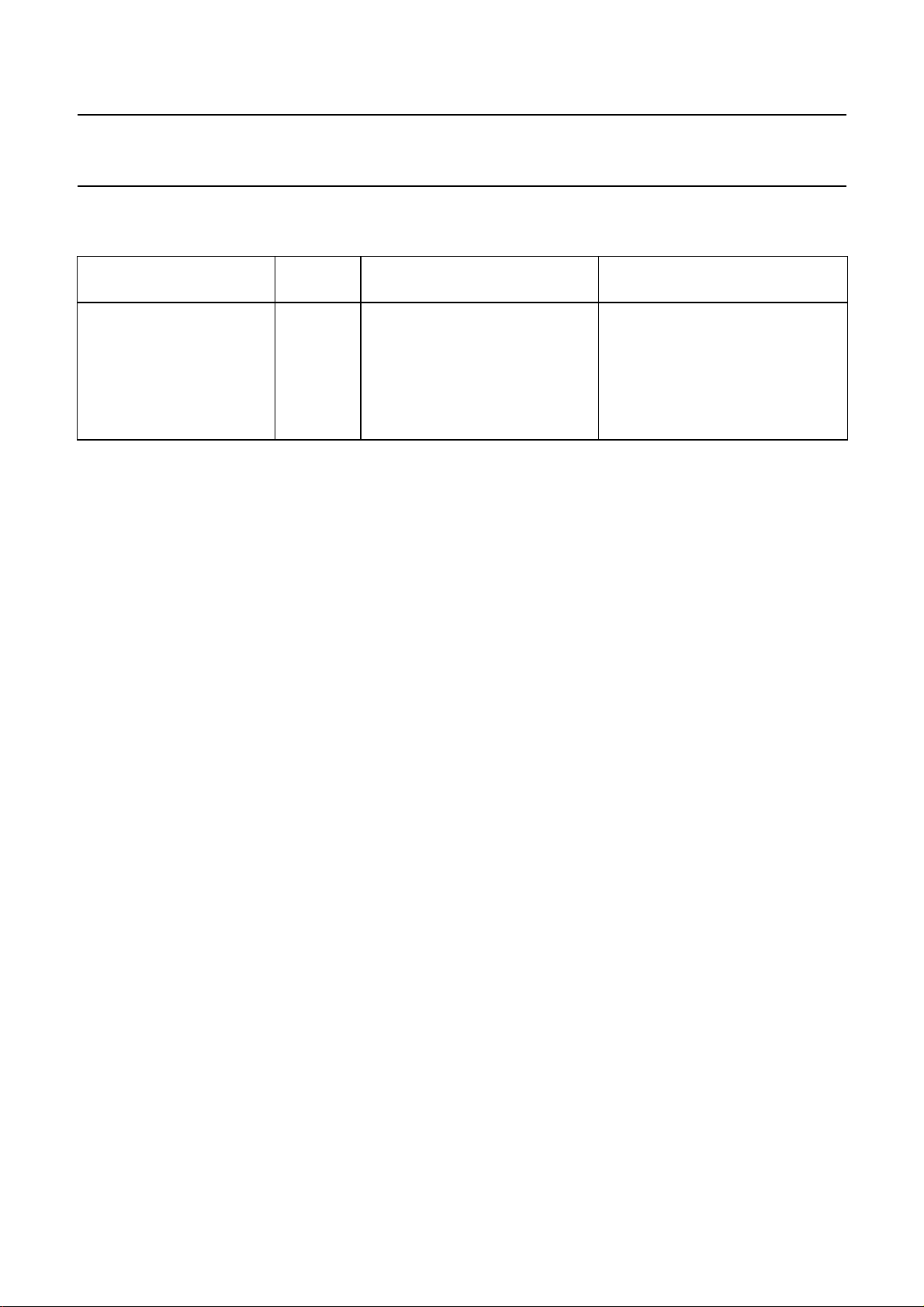
AC CHARACTERISTICS
V
= 0 V; T
SS
Dynamic power 5 1 050 f
dissipation per 10 4 500 f
package (P) 15 10 500 f
=25°C; input transition times ≤ 20 ns
amb
V
DD
V
TYPICAL FORMULA FOR P (µW)
+∑(foCL) × V
i
+∑(foCL) × V
i
+∑(foCL) × V
i
DD
DD
DD
2
where
2
fi= input freq. (MHz)
2
fo= output freq. (MHz)
= load capacitance (pF)
C
L
∑ (f
oCL
V
= supply voltage (V)
DD
HEF4527B
MSI
) = sum of outputs
January 1995 8
Page 9
Philips Semiconductors Product specification
BCD rate multiplier
HEF4527B
MSI
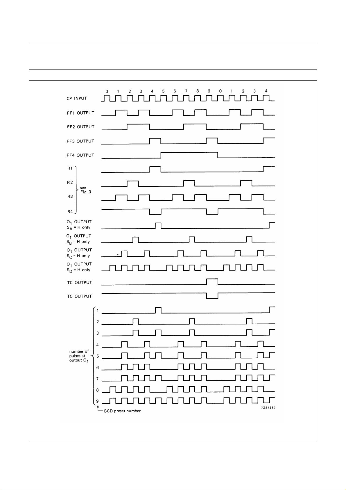
Fig.4 Timing diagram.
January 1995 9
Page 10
Philips Semiconductors Product specification
BCD rate multiplier
APPLICATION INFORMATION
Add mode
HEF4527B
MSI
Output rate = 10n(0,1 BCD1+ 0,01 BCD2+ 0,01 BCD3+ ........), in where n = number of cascaded RMs.
Example: RM1 preset to 9 and RM2 preset to 4, output rate is 10
2
(0,1 × 9 + 0,01 × 4) = 94.
Fig.5 Two HEF4527B cascaded in the add mode.
Multiply mode
Output rate = 10n(0,1 BCD1× 0,1 BCD2× 0,1 BCD3× ........), in where n = number of cascaded RMs.
Example: RM1 preset to 9 and RM2 preset to 4, output rate is 10
2
(0,1 × 9 × 0,1 × 4) = 36.
Fig.6 Two HEF4527B cascaded in the multiply mode.
January 1995 10
 Loading...