

Page 1

INTEGRATED CIRCUITS
DATA SH EET
For a complete data sheet, please also download:
•The IC04 LOCMOS HE4000B Logic
Family Specifications HEF, HEC
•The IC04 LOCMOS HE4000B Logic
Package Outlines/Information HEF, HEC
HEF4060B
MSI
14-stage ripple-carry binary
counter/divider and oscillator
Product specification
File under Integrated Circuits, IC04
January 1995
Page 2

Philips Semiconductors Product specification
14-stage ripple-carry binary
counter/divider and oscillator
DESCRIPTION
The HEF4060B is a 14-stage ripple-carry binary
counter/divider and oscillator with three oscillator terminals
(RS, RTCand CTC), ten buffered outputs (O3to O9and
O11to O13) and an overriding asynchronous master reset
input (MR). The oscillator configuration allows design of
either RC or crystal oscillator circuits. The oscillator may
HEF4060B
MSI
be replaced by an external clock signal at input RS. The
counter advances on the negative-going transition of RS.
A HIGH level on MR resets the counter (O
O11to O13= LOW), independent of other input conditions.
Schmitt-trigger action in the clock input makes the circuit
highly tolerant to slower clock rise and fall times.
to O9and
3
Fig.2 Pinning diagram.
Fig.1 Functional diagram.
PINNING
MR master reset
RS clock input/oscillator pin
R
TC
C
TC
to O
O
3
9
O
to O
11
13
HEF4060BP(N): 16-lead DIL; plastic (SOT38-1)
HEF4060BD(F): 16-lead DIL; ceramic (cerdip) (SOT74)
HEF4060BT(D): 16-lead SO; plastic (SOT109-1)
( ): Package Designator North America
FAMILY DATA, I
See Family Specifications
oscillator pin
external capacitor connection
counter outputs
LIMITS category MSI
DD
January 1995 2
Page 3

This text is here in white to force landscape pages to be rotated correctly when browsing through the pdf in the Acrobat reader.This text is here in
_white to force landscape pages to be rotated correctly when browsing through the pdf in the Acrobat reader.This text is here inThis text is here in
white to force landscape pages to be rotated correctly when browsing through the pdf in the Acrobat reader. white to force landscape pages to be ...
January 1995 3
Philips Semiconductors Product specification
14-stage ripple-carry binary counter/divider
and oscillator
Fig.3 Logic diagram.
HEF4060B
MSI
Page 4
Philips Semiconductors Product specification
14-stage ripple-carry binary counter/divider
HEF4060B
and oscillator
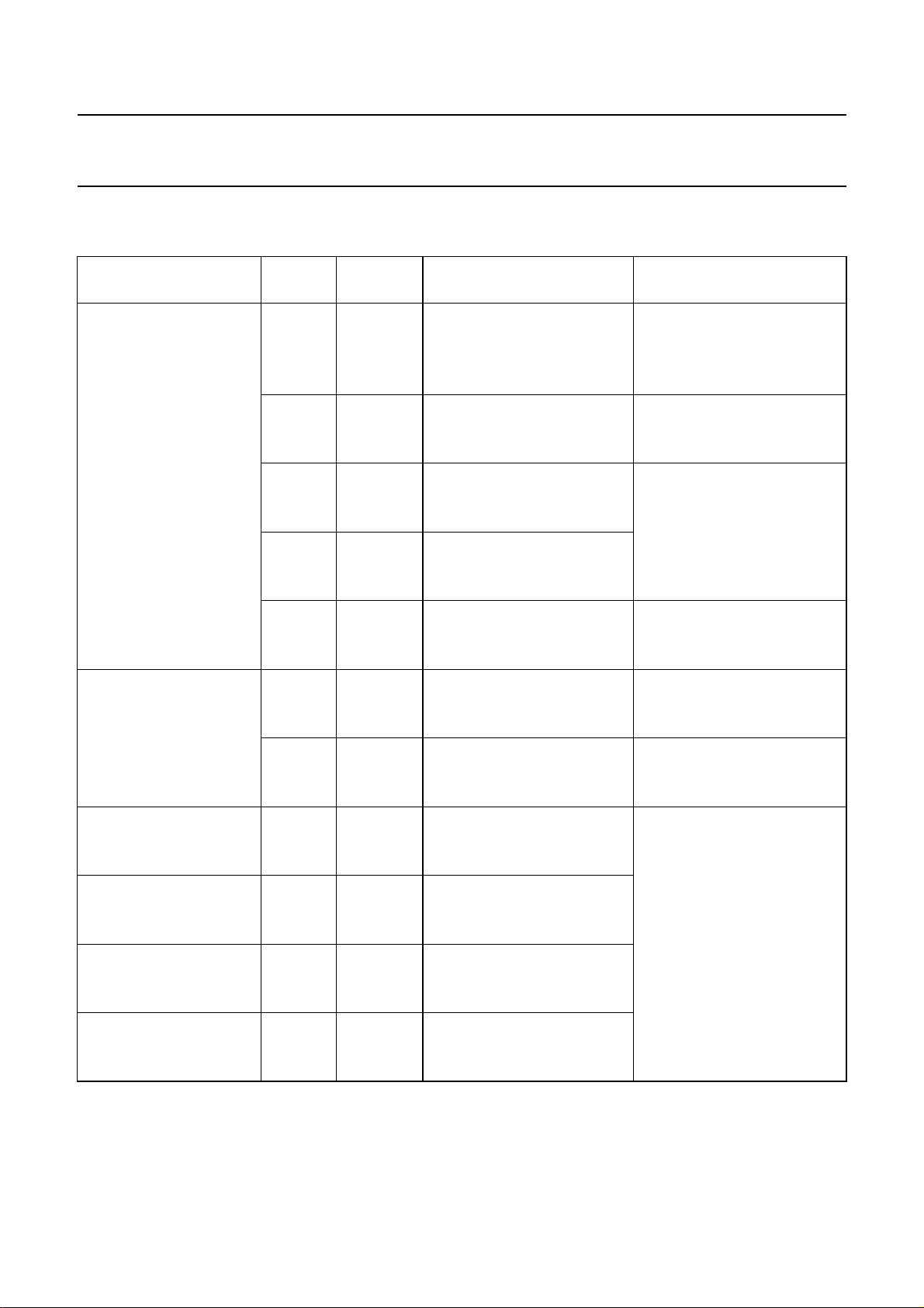
AC CHARACTERISTICS
V
= 0 V; T
SS
Propagation delays
RS → O
HIGH to LOW 10 t
LOW to HIGH 10 t
On→ O
HIGH to LOW 10 t
LOW to HIGH 10 t
MR → O
HIGH to LOW 10 t
Output transition 5 60 120 ns 10 ns + (1,0 ns/pF) C
times 10 t
HIGH to LOW 15 20 40 ns 6 ns + (0,28 ns/pF) C
LOW to HIGH 10 t
Minimum clock pulse 5 120 60 ns
width input RS 10 t
HIGH 15 30 15 ns
Minimum MR pulse 5 50 25 ns
width; HIGH 10 t
Recovery time 5 160 80 ns
for MR 10 t
Maximum clock pulse 5 4 8 MHz
frequency input RS 10 f
=25°C; CL= 50 pF; input transition times ≤ 20 ns
amb
V
DD
V
3
SYMBOL MIN. TYP. MAX.
5 210 420 ns 183 ns + (0,55 ns/pF) C
PHL
15 50 100 ns 42 ns + (0,16 ns/pF) C
5 210 420 ns 183 ns + (0,55 ns/pF) C
PLH
15 50 100 ns 42 ns + (0,16 ns/pF) C
n + 1
52550ns
PHL
15 6 12 ns
52550ns
PLH
15 6 12 ns
n
5 100 200 ns 73 ns + (0,55 ns/pF) C
PHL
15 30 60 ns 22 ns + (0,16 ns/pF) C
THL
5 60 120 ns 10 ns + (1,0 ns/pF) C
TLH
15 20 40 ns 6 ns + (0,28 ns/pF) C
WRSH
WMRH
15 20 10 ns
RMR
15 60 30 ns
max
15 15 30 MHz
TYPICAL EXTRAPOLATION
FORMULA
80 160 ns 69 ns + (0,23 ns/pF) C
80 160 ns 69 ns + (0,23 ns/pF) C
10 20 ns
10 20 ns
40 80 ns 29 ns + (0,23 ns/pF) C
30 60 ns 9 ns + (0,42 ns/pF) C
30 60 ns 9 ns + (0,42 ns/pF) C
50 25 ns
30 15 ns
80 40 ns
10 20 MHz
MSI
L
L
L
L
L
L
L
L
L
L
L
L
L
L
L
January 1995 4
Page 5
Philips Semiconductors Product specification
14-stage ripple-carry binary counter/divider
and oscillator
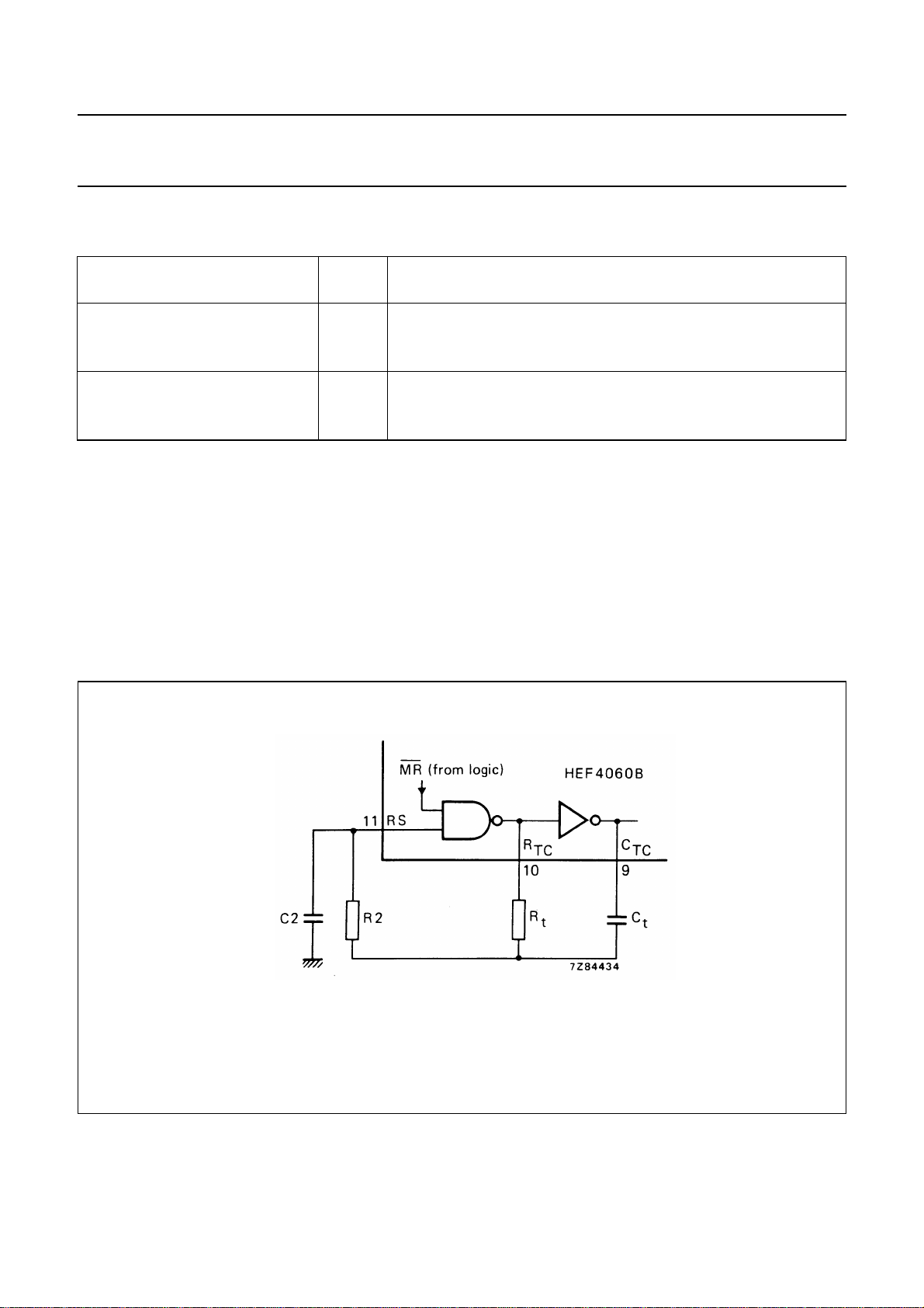
AC CHARACTERISTICS
V
= 0 V; T
SS
Dynamic power dissipation 5 700 fi+ foCLV
per package 10 3 300 fi+ foCLV
(P) 15 8 900 fi+ foCLV
Total power dissipation 5 700 f
when using the 10 3 300 f
on-chip oscillator (P) 15 8 900 f
Notes
1. where:
f
= input frequency (MHz)
i
fo= output frequency (MHz)
CL= load capacitance (pF)
VDD= supply voltage (V)
Ct= timing capacitance (pF)
f
= oscillator frequency (MHz)
osc
=25°C; input transition times ≤ 20 ns
amb
V
DD
V
TYPICAL FORMULA FOR P (µW)
+ foCLV
osc
+ foCLV
osc
+ foCLV
osc
DD
DD
DD
HEF4060B
MSI
(1)
2
2
2
DD
DD
DD
2
2
2
+ 2CtV
+ 2CtV
+ 2CtV
DD
DD
DD
2
f
osc
2
f
osc
2
f
osc
+ 690 V
+ 6 900 V
+ 22 000 V
DD
DD
DD
RC oscillator
Typical formula for oscillator frequency:
-------------------------------- -=
2,3 RtCt××
1
f
osc
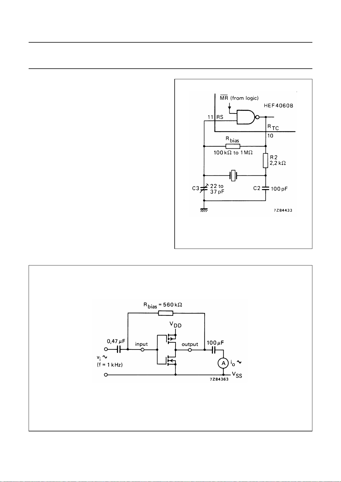
Fig.4 External component connection for RC oscillator.
January 1995 5
Page 6
Philips Semiconductors Product specification
14-stage ripple-carry binary counter/divider
and oscillator
Timing component limitations
The oscillator frequency is mainly determined by
RtCt, provided Rt<< R2 and R2C2 << RtCt. The function
of R2 is to minimize the influence of the forward voltage
across the input protection diodes on the frequency. The
stray capacitance C2 should be kept as small as possible.
In consideration of accuracy, Ctmust be larger than the
inherent stray capacitance. Rtmust be larger than the
LOCMOS ‘ON’ resistance in series with it, which typically
is 500 Ω at VDD= 5 V, 300 Ω at VDD= 10 V and 200 Ω at
= 15 V.
V
DD
The recommended values for these components to
maintain agreement with the typical oscillation formula are:
Ct≥ 100 pF, up to any practical value,
10 kΩ≤Rt≤1 MΩ.
Typical crystal oscillator circuit
In Fig.5, R2 is the power limiting resistor. For starting and
maintaining oscillation a minimum transconductance is
necessary.
HEF4060B
MSI
Fig.5 External component connection for crystal
oscillator.
Fig.6 Test set-up for measuring forward transconductance gfs=dio/dviat vois constant (see also graph Fig.7);
MR = LOW.
January 1995 6
Page 7
Philips Semiconductors Product specification
14-stage ripple-carry binary counter/divider
and oscillator
HEF4060B
MSI
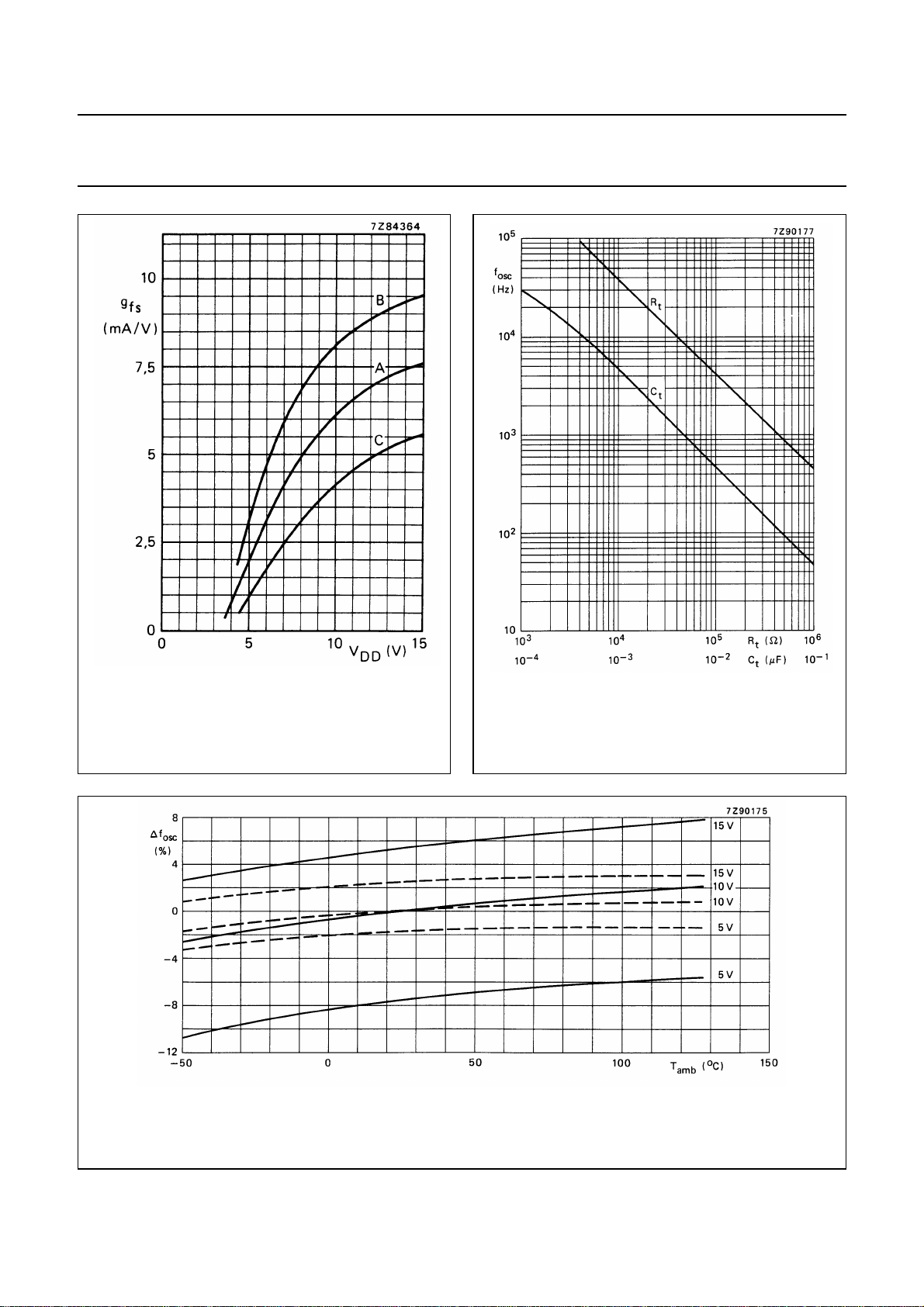
A: average
B: average + 2 s,
C: average − 2 s, where ‘s’ is the observed standard deviation.
Fig.7 Typical forward transconductance gfsas a
function of the supply voltage at T
___ Rt= 100 kΩ; Ct= 1 nF; R2 = 0.
--- Rt= 100 kΩ;Ct= 1 nF; R2 = 300 kΩ.
Fig.9 Oscillator frequency deviation (∆f
T
=25°C and VDD= 10 V.
amb
= 25 °C.
amb
) as a function of ambient temperature; referenced at: f
osc
Ctcurve at Rt= 100 kΩ; R2 = 470 kΩ.
Rtcurve at Ct= 1 nF; R2 = 5 Rt.
Fig.8 RC oscillator frequency as a function of
Rtand Ctat VDD= 5 to 15 V; T
osc
amb
at
=25°C.
January 1995 7
 Loading...