

Page 1

INTEGRATED CIRCUITS
DATA SH EET
For a complete data sheet, please also download:
•The IC04 LOCMOS HE4000B Logic
Family Specifications HEF, HEC
•The IC04 LOCMOS HE4000B Logic
Package Outlines/Information HEF, HEC
HEF4052B
MSI
Dual 4-channel analogue
multiplexer/demultiplexer
Product specification
File under Integrated Circuits, IC04
January 1995
Page 2
Philips Semiconductors Product specification
Dual 4-channel analogue multiplexer/demultiplexer
DESCRIPTION
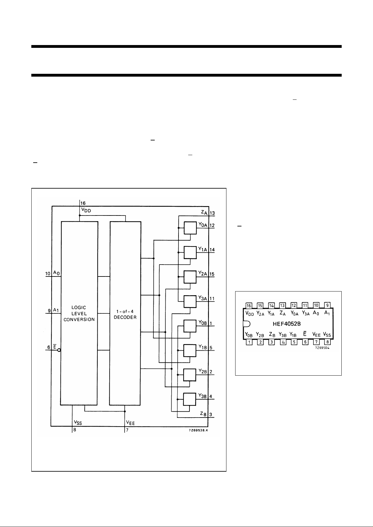
The HEF4052B is a dual 4-channel
analogue multiplexer/demultiplexer
with common channel select logic.
Each multiplexer/demultiplexer has
four independent inputs/outputs
(Y0to Y3) and a common input/output
(Z). The common channel select logic
includes two address inputs (A0and
A1) and an active LOW enable input
E).
(
Both multiplexers/demultiplexers
contain four bidirectional analogue
switches, each with one side
connected to an independent
input/output (Y
to Y3) and the other
0
side connected to a common
input/output (Z).
With E LOW, one of the four switches
is selected (low impedance ON-state)
by A0and A1. With E HIGH, all
switches are in the high impedance
OFF-state, independent of A0and A1.
HEF4052B
MSI
VDDand VSSare the supply voltage
connections for the digital control
inputs (A0,A1 and E). The VDDto
VSSrange is 3 to 15 V. The analogue
inputs/outputs (Y0to Y3, and Z) can
swing between VDDas a positive limit
and VEEas a negative limit.
VDD− VEEmay not exceed 15 V.
For operation as a digital
multiplexer/demultiplexer, VEEis
connected to VSS(typically ground).
PINNING
Y
to Y
0A
to Y
Y
0B
A
, A
0
1
E enable input (active LOW)
Z
, Z
A
B
independent inputs/outputs
3A
independent inputs/outputs
3B
address inputs
common inputs/outputs
Fig.1 Functional diagram.
FAMILY DATA,
I
LIMITS category MSI
DD
See Family Specifications
Fig.2 Pinning diagram.
HEF4052BP(N): 16-lead DIL; plastic
(SOT38-1)
HEF4052BD(F): 16-lead DIL; ceramic
(cerdip)
(SOT74)
HEF4052BT(D): 16-lead SO; plastic
(SOT109-1)
( ): Package Designator North America
January 1995 2
Page 3
Philips Semiconductors Product specification
Dual 4-channel analogue multiplexer/demultiplexer
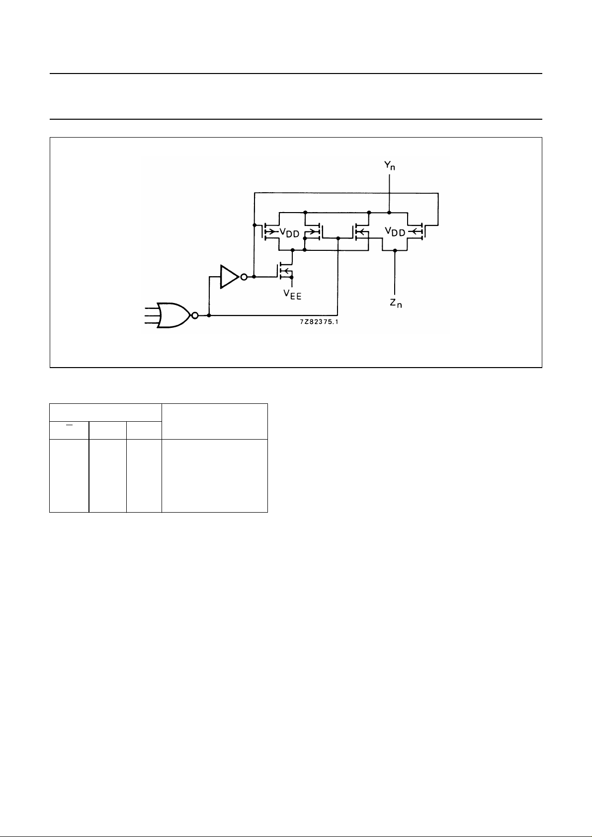
Fig.3 Schematic diagram (one switch).
HEF4052B
MSI
FUNCTION TABLE
INPUTS CHANNEL
0A−ZA
1A−ZA
2A−ZA
3A−ZA
ON
; Y0B−Z
; Y1B−Z
; Y2B−Z
; Y3B−Z
B
B
B
B
EA
1
A
0
LLLY
LLHY
LHL Y
LHHY
H X X none
Notes
1. H = HIGH state (the more positive voltage)
L = LOW state (the less positive voltage)
X = state is immaterial
RATINGS
Limiting values in accordance with the Absolute Maximum System (IEC 134)
Supply voltage (with reference to VDD)V
EE
−18 to + 0,5 V
Note
1. To avoid drawing V
current out of terminal Z, when switch current flows into terminals Y, the voltage drop across
DD
the bidirectional switch must not exceed 0,4 V. If the switch current flows into terminal Z, no VDDcurrent will flow out
of terminals Y, in this case there is no limit for the voltage drop across the switch, but the voltages at Y and Z may
not exceed VDDor VEE.
January 1995 3
Page 4
Philips Semiconductors Product specification
Dual 4-channel analogue multiplexer/demultiplexer
HEF4052B
MSI
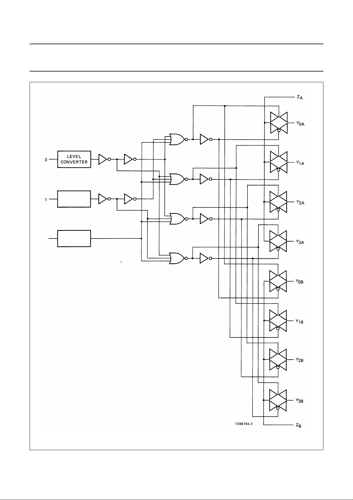
Fig.4 Logic diagram.
January 1995 4
Page 5
Philips Semiconductors Product specification
Dual 4-channel analogue multiplexer/demultiplexer
DC CHARACTERISTICS
T
=25°C
amb
V
DD−VEE
V
5 350 2500 Ω
ON resistance 10 R
15 60 175 Ω
5 115 340 Ω
ON resistance 10 R
15 40 115 Ω
5 120 365 Ω
ON resistance 10 R
15 50 155 Ω
‘∆’ ON resistance 5 25 −Ω
between any two 10 ∆R
channels 15 5 −Ω
OFF-state leakage 5 −−nA
current, all 10 I
channels OFF 15 − 1000 nA
OFF-state leakage 5 −−nA
current, any 10 I
channel 15 − 200 nA
SYMBOL TYP. MAX. CONDITIONS
ON
ON
ON
ON
OZZ
OZY
80 245 Ω
50 160 Ω
65 200 Ω
10 −Ω
−−nA
−−nA
= 0 to VDD−V
V
is
see Fig.6
V
=0
is
see Fig.6
V
is=VDD−VEE
see Fig.6
V
= 0 to VDD−V
is
see Fig.6
E at V
DD
E at V
SS
HEF4052B
MSI
EE
EE
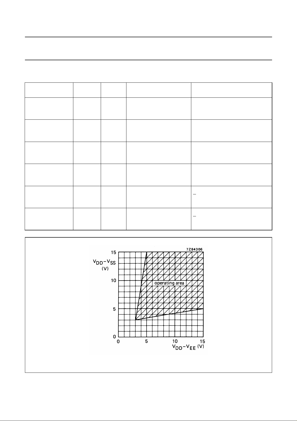
Fig.5 Operating area as a function of the supply voltages.
January 1995 5
Page 6
Philips Semiconductors Product specification
Dual 4-channel analogue multiplexer/demultiplexer
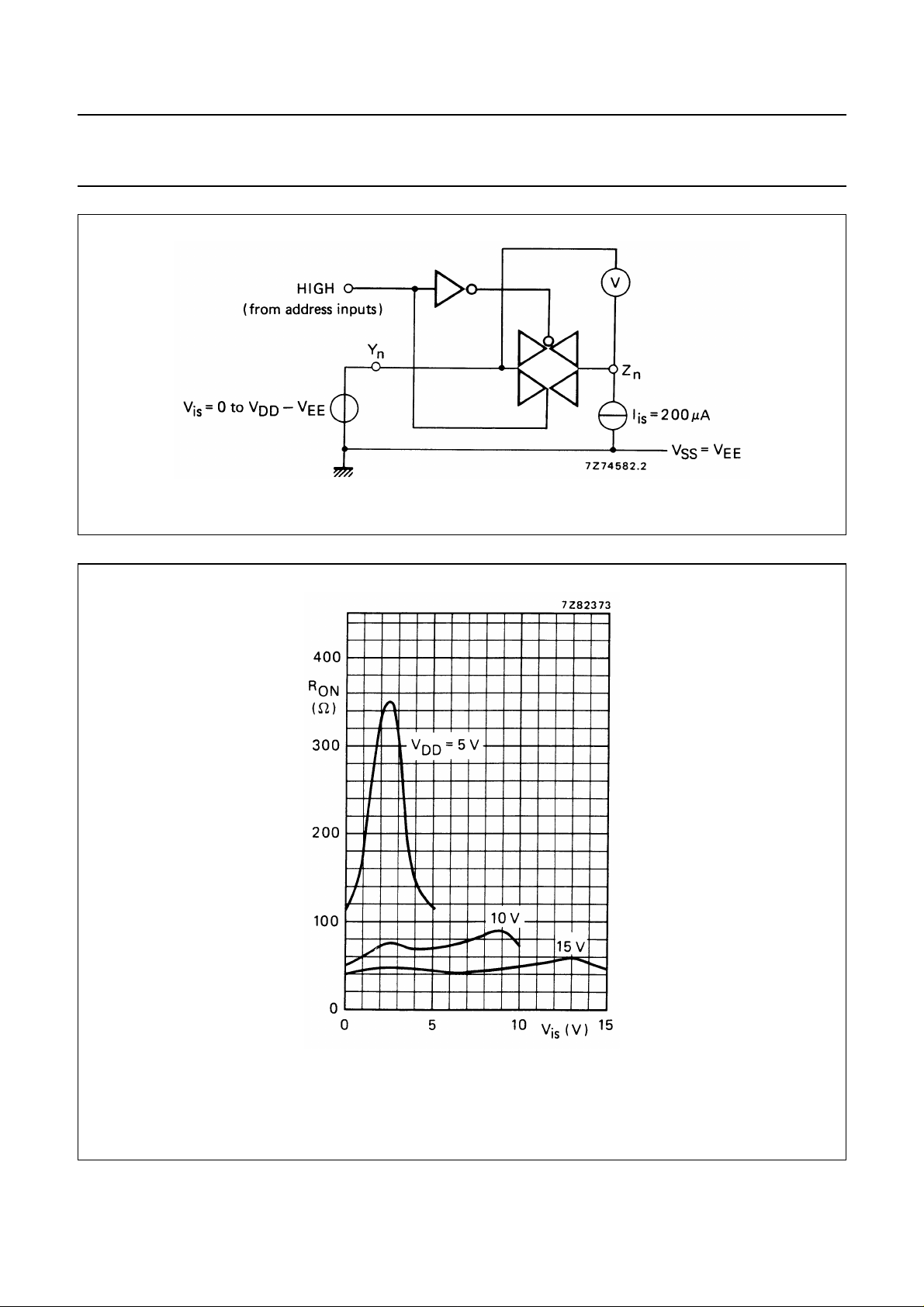
Fig.6 Test set-up for measuring RON.
HEF4052B
MSI
Iis= 200 µA
VSS=VEE=0 V
Fig.7 Typical RONas a function of input voltage.
January 1995 6
Page 7
Philips Semiconductors Product specification
Dual 4-channel analogue multiplexer/demultiplexer
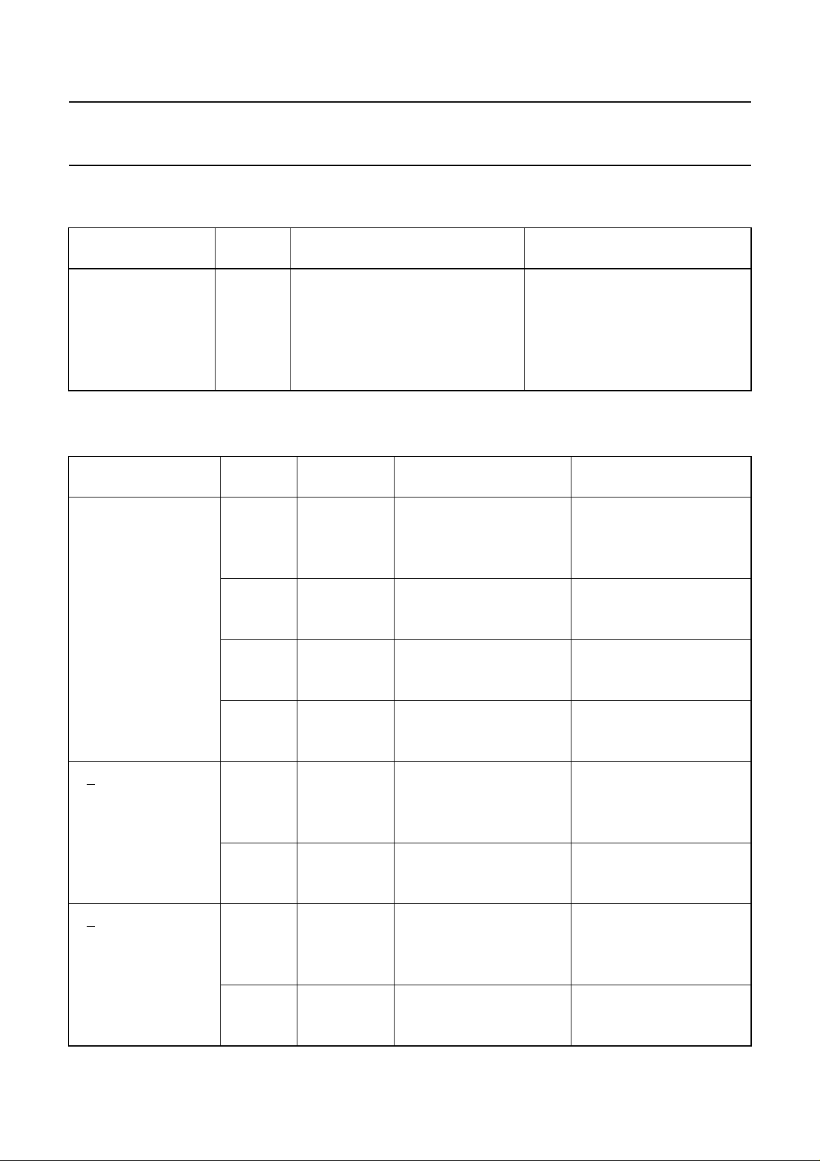
AC CHARACTERISTICS
V
EE=VSS
Dynamic power 5 1 300 f
dissipation per 10 6 100 f
package (P) 15 15 600 f
AC CHARACTERISTICS
V
EE=VSS
Propagation delays
Vis→ V
A
Output disable times
E → V
Output enable times
E → V
n
→ V
= 0 V; T
= 0 V; T
os
os
os
os
=25°C; input transition times ≤ 20 ns
amb
V
DD
V
=25°C; input transition times ≤ 20 ns
amb
V
DD
V
TYPICAL FORMULA FOR P (µW)
SYMBOL TYP. MAX.
51020ns
PHL
15 5 10 ns
51020ns
PLH
15 5 10 ns
5 150 305 ns
PHL
15 50 100 ns
5 150 300 ns
PLH
15 50 100 ns
5 95 190 ns
PHZ
15 90 180 ns
5 100 205 ns
PLZ
15 90 180 ns
5 130 260 ns
PZH
15 45 85 ns
5 120 240 ns
PZL
15 35 75 ns
+∑(foCL) × V
i
+∑(foCL) × V
i
+∑(foCL) × V
i
510ns
510ns
65 135 ns
75 150 ns
90 180 ns
90 180 ns
55 115 ns
50 100 ns
DD
DD
DD
2
2
2
HEF4052B
where
fi= input freq. (MHz)
fo= output freq. (MHz)
= load capacitance (pF)
C
L
∑(f
) = sum of outputs
oCL
V
= supply voltage (V)
DD
note 1HIGH to LOW 10 t
note 1LOW to HIGH 10 t
note 2HIGH to LOW 10 t
note 2LOW to HIGH 10 t
note 3HIGH 10 t
note 3LOW 10 t
note 3HIGH 10 t
note 3LOW 10 t
MSI
January 1995 7
Page 8

Philips Semiconductors Product specification
Dual 4-channel analogue multiplexer/demultiplexer
V
DD
V
Distortion, sine-wave 5 0,25 %
15 0,04 %
Crosstalk between 5 − MHz
15 − MHz
Crosstalk; enable 5 − mV
to output 15 − mV
OFF-state 5 − MHz
15 − MHz
ON-state frequency 5 13 MHz
15 70 MHz
SYMBOL TYP. MAX.
HEF4052B
MSI
note 4response 10 0,04 %
note 5any two channels 10 1 MHz
note 6or address input 10 50 mV
note 7feed-through 10 1 MHz
note 8response 10 40 MHz
Notes
Visis the input voltage at a Y or Z terminal, whichever is assigned as input.
Vosis the output voltage at a Y or Z terminal, whichever is assigned as output.
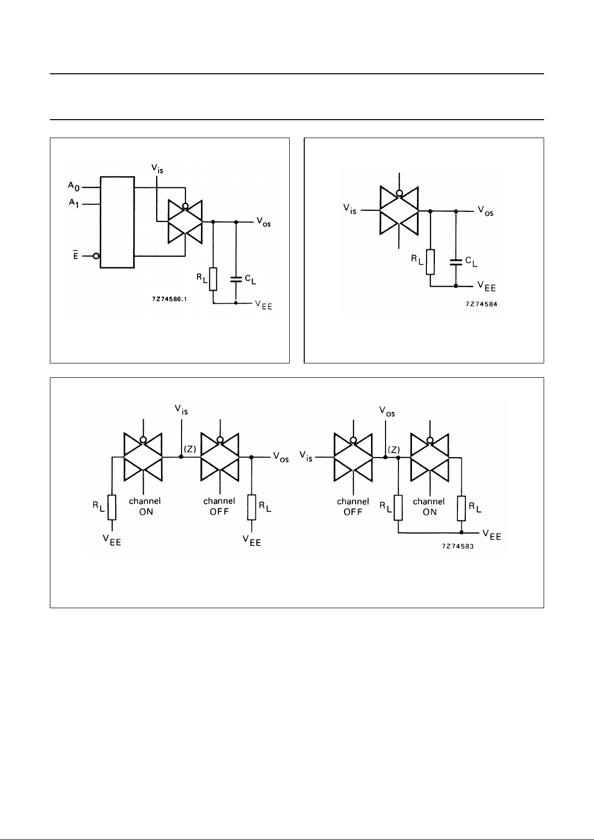
1. RL= 10 kΩ to VEE; CL= 50 pF to VEE; E=VSS; Vis=VDD(square-wave); see Fig.8.
2. RL= 10 kΩ; CL= 50 pF to VEE; E=VSS; An=VDD(square-wave); Vis=VDDand RLto VEEfor t
RLto VDDfor t
; see Fig.8.
PHL
3. RL= 10 kΩ; CL= 50 pF to VEE; E=VDD(square-wave);
Vis=VDDand RLto VEEfor t
Vis=VEEand RLto VDDfor t
4. RL= 10 kΩ; CL= 15 pF; channel ON; Vis=1⁄2V
PHZ
PLZ
and t
and t
;
PZH
; see Fig.8.
PZL
DD (p-p)
(sine-wave, symmetrical about1⁄2VDD);
fis= 1 kHz; see Fig.9.
5. RL=1 kΩ; Vis=1⁄2V
V
os
20 log
-------- -
V
50 dB; see Fig. 10.–=
is
(sine-wave, symmetrical about1⁄2VDD);
DD (p-p)
6. RL= 10 kΩ to VEE; CL= 15 pF to VEE; E or An=VDD(square-wave); crosstalk is Vos (peak
value); see Fig.8.
7. RL=1 kΩ; CL= 5 pF; channel OFF; Vis=1⁄2V
V
os
-------- -
20 log
V
50 dB; see Fig. 9.–=
is
(sine-wave, symmetrical about1⁄2VDD);
DD (p-p)
; Vis=VEEand
PLH
8. RL=1 kΩ; CL= 5 pF; channel ON; Vis=1⁄2V
V
os
20 log
-------- -
V
3 dB; see Fig. 9.–=
is
(sine-wave, symmetrical about1⁄2VDD);
DD (p-p)
January 1995 8
Page 9
Philips Semiconductors Product specification
Dual 4-channel analogue multiplexer/demultiplexer
Fig.8 Fig.9
HEF4052B
MSI
(a)
Fig.10
APPLICATION INFORMATION
Some examples of applications for the HEF4052B are:
• Analogue multiplexing and demultiplexing.
• Digital multiplexing and demultiplexing.
• Signal gating.
NOTE
If break before make is needed, then it is necessary to use the enable input.
January 1995 9
(b)
 Loading...