

Page 1

DATA SH EET
Product specification
File under Integrated Circuits, IC04
January 1995
INTEGRATED CIRCUITS
HEF4000B
gates
Dual 3-input NOR gate and inverter
For a complete data sheet, please also download:
•The IC04 LOCMOS HE4000B Logic
Family Specifications HEF, HEC
•The IC04 LOCMOS HE4000B Logic
Package Outlines/Information HEF, HEC
Page 2
January 1995 2
Philips Semiconductors Product specification
Dual 3-input NOR gate and inverter
HEF4000B
gates
DESCRIPTION
The HEF4000B provides the positive dual 3-input NOR
function. A single stage inverting function with standard
output performance is also accomplished. The outputs are
fully buffered for highest noise immunity and pattern
insensitivity of output impedance.
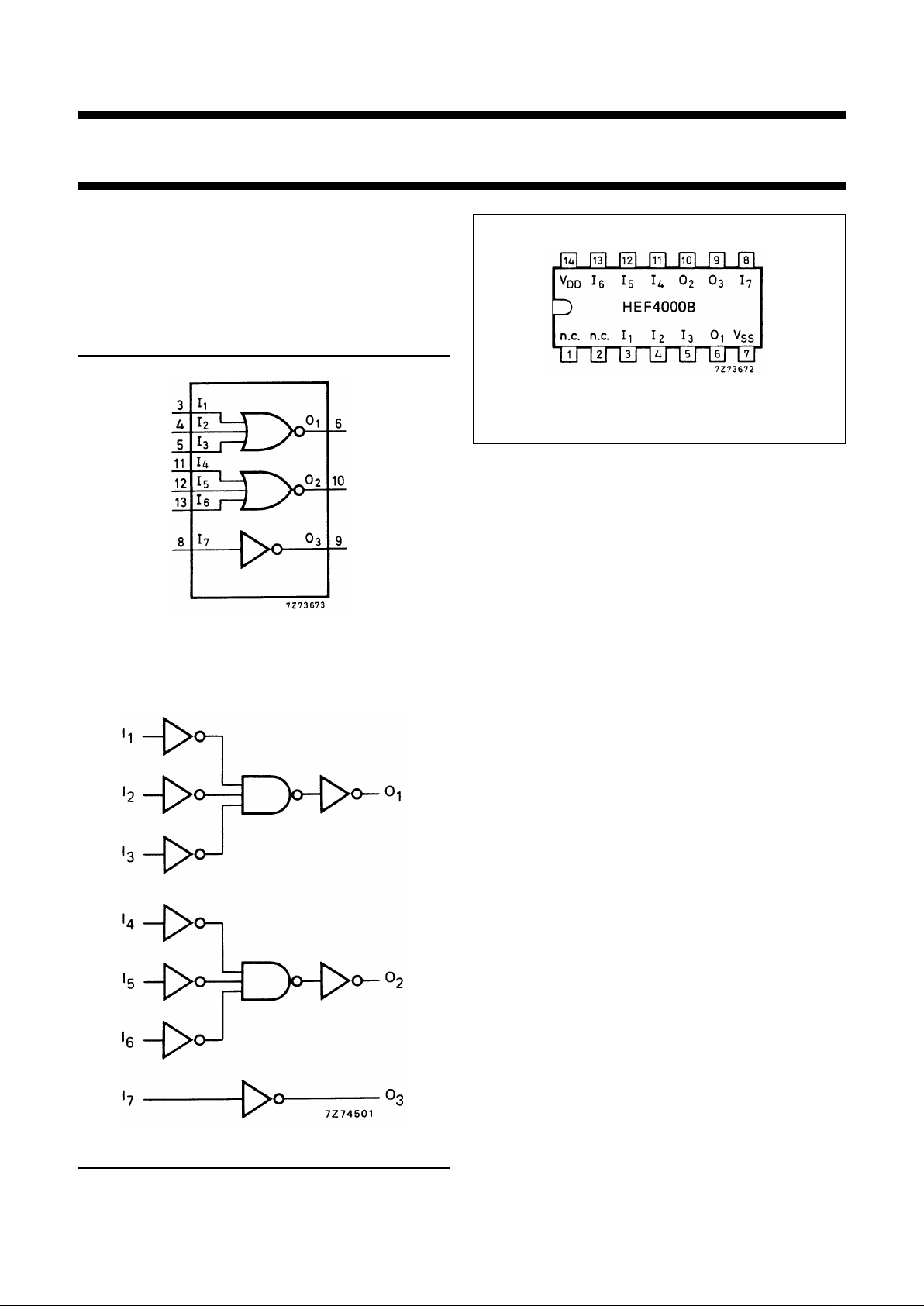
Fig.1 Functional diagram.
HEF4000BP(N): 14-lead DIL; plastic
(SOT27-1)
HEF4000BD(F): 14-lead DIL; ceramic (cerdip)
(SOT73)
HEF4000BT(D): 14-lead SO; plastic
(SOT108-1)
( ): Package Designator North America
Fig.2 Pinning diagram.
Fig.3 Logic diagram.
FAMILY DATA, IDDLIMITS category GATES
See Family Specifications
Page 3

January 1995 3
Philips Semiconductors Product specification
Dual 3-input NOR gate and inverter
HEF4000B
gates
DC CHARACTERISTICS
For the single inverter stage (I7/O3):
see Family Specifications for input voltages HIGH and LOW (unbuffered stages only).
AC CHARACTERISTICS
V
SS
= 0 V; T
amb
=25°C; CL= 50 pF; input transition times ≤20 ns
V
DD
V
SYMBOL TYP. MAX.
TYPICAL EXTRAPOLATION
FORMULA
Propagation delays 5 70 140 ns 43 ns + (0,55 ns/pF) C
L
I1to I6→ O1,O
2
10 t
PHL
; t
PLH
35 70 ns 24 ns + (0,23 ns/pF) C
L
15 30 55 ns 22 ns + (0,16 ns/pF) C
L
5 45 90 ns 18 ns + (0,55 ns/pF) C
L
I7→ O
3
10 t
PHL
; t
PLH
25 50 ns 14 ns + (0,23 ns/pF) C
L
(unbuffered output) 15 20 40 ns 12 ns + (0,16 ns/pF) C
L
Output transition times 5 60 120 ns 10 ns + (1,0 ns/pF) C
L
HIGH to LOW 10 t
THL
30 60 ns 9 ns + (0,42 ns/pF) C
L
15 20 40 ns 6 ns + (0,28 ns/pF) C
L
5 60 120 ns 10 ns + (1,0 ns/pF) C
L
LOW to HIGH 10 t
TLH
30 60 ns 9 ns + (0,42 ns/pF) C
L
15 20 40 ns 6 ns + (0,28 ns/pF) C
L
V
DD
V
TYPICAL FORMULA FOR P (µW)
Dynamic power 5 1 000 f
i
+∑(foCL) × V
DD
2
where
dissipation per 10 7 700 f
i
+∑(foCL) × V
DD
2
fi= input freq. (MHz)
package (P) 15 28 700 f
i
+∑(foCL) × V
DD
2
fo= output freq. (MHz)
C
L
= load capacitance (pF)
∑ (f
oCL
) = sum of outputs
V
DD
= supply voltage (V)
Page 4

January 1995 4
Philips Semiconductors Product specification
Dual 3-input NOR gate and inverter
HEF4000B
gates
APPLICATION INFORMATION
The following information (Figs 4 to 7) is only for the single
inverter stage (I7/O3).
Fig.4 Voltage gain (VO/VI) as a function of supply
voltage.
Fig.5 Supply current as a function of supply
voltage.
Fig.6 Test set-up for measuring graphs of Figs 4
and 5.
This is also an example of an analogue amplifier using the
single inverter stage (I7/O3) of the HEF4000B.
Page 5

January 1995 5
Philips Semiconductors Product specification
Dual 3-input NOR gate and inverter
HEF4000B
gates
Fig.7 Test set-up for measuring forward transconductance gfs=dio/dviat vois constant (see also graph Fig.8).
Fig.8 Typical forward transconductance gfsas a function of the supply voltage at T
amb
=25°C.
A: average
B: average + 2 s,
C: average − 2 s, in where ‘s’ is the observed standard deviation.
 Loading...