

Page 1
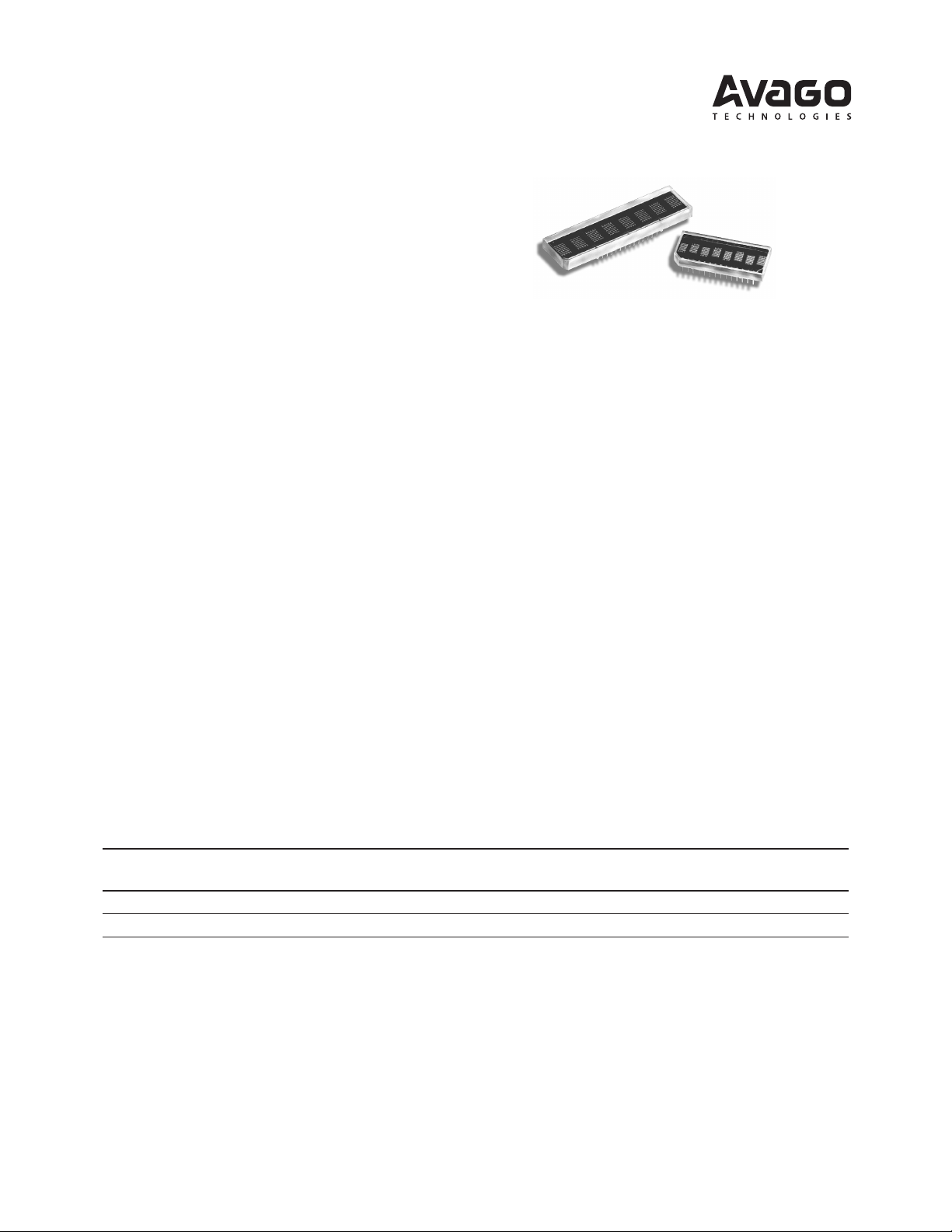
HDSP-210x Series
Eight Character 5 mm and 7 mm Smart
Alphanumeric Displays
Data Sheet
HDSP-210x Series, HDSP-211x Series, HDSP-250x Series
Description
The HDSP-210x/-211x/-250x series of products is
ideal for applications where displaying e ight or
more characters of dot matrix information in an aesthetically pleasing manner is required. These devices are
8-digit, 5 x 7 dot matrix, alphanumeric displays and are
all packaged in a standard 15.24 mm (0.6 inch) 28 pin
DIP. The on-board CMOS IC has the ability to decode 128
ASCII characters which are permanently stored in ROM.
In addition, 16 programmable symbols may be stored in
on- board ROM, allowing considerable exibility for displaying additional symbols and icons. Seven brightness
levels provide versatility in adjusting the display intensity
and power consumption. The HDSP-210x/-211x/-250x
products are designed for standard microprocessor
interface techniques. The display and special features are
accessed through a bidirectional 8-bit data bus.
Features
• X stackable (HDSP-21xx)
• XY stackable (HDSP-250x)
• 128 sharacter ASCII decoder
• Programmable functions
• 16 user denable characters
• Multi-level dimming and blanking
• TTL compatible CMOS IC
• Wave solderable
Applications
• Computer peripherals
• Industrial instrumentation
• Medical equipment
• Portable data entry devices
• Cellular phones
• Telecommunications equipment
• Test equipment
Device Selection Guide
AlGaAs High Eciency
Font Height Red Red Orange Yellow Green
0.2 inches HDSP-2107 HDSP-2112 HDSP-2110 HDSP-2111 HDSP-2113
0.27 inches HDSP-2504 HDSP-2502 HDSP-2500 HDSP-2501 HDSP-2503
Page 2
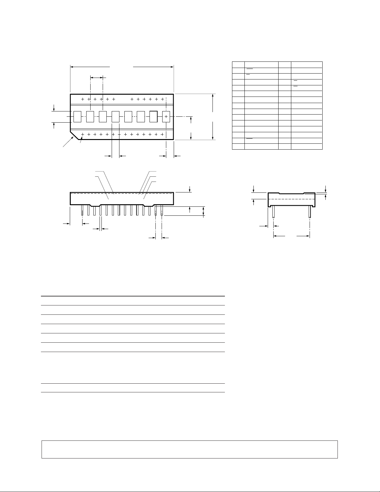
Package Dimensions
SYM.
TYP.
TYP. (NON-ACCUM)
LUMINOUS INTENSITY CATEGORY
COLOR BIN (NOTE 3)
COUNTRY OF ORIGIN
2.17
(0.085)
IMAGE PLANE
(FOR REFERENCE ONLY)
2.01 (0.08)
5.31
(0.209)
9.8
(0.386)
4.81
(0.189)
[4]
3.92
(0.154)
SYM.
4.79
(0.189)
2.54 ± 0.13
(0.100 ± 0.005)
TYP.
DIA.
0.51 ± 0.13
(0.020 ± 0.005)
PART NUMBER
15.24
(0.600)
0.25
(0.010)
PIN # FUNCTION PIN # FUNCTION
1
2
3
4
5
6
7
8
9
10
11
12
13
14
RST
FL
A
0
A
1
A
2
A
3
DO NOT CONNECT
DO NOT CONNECT
DO NOT CONNECT
A
4
CLS
CLK
WR
V
DD
15
16
17
18
19
20
21
22
23
24
25
26
27
28
GND (SUPPLY)
GND (LOGIC)
CE
RD
D
0
D
1
NO PIN
NO PIN
D
2
D
3
D
4
D
5
D
6
D
7
PIN FUNCTION ASSIGNMENT TABLE
3 4 5
6
7
19.58
(0.771)
2.69
(0.106)
42.59 (1.677)
TYP.
5.33
(0.210)
SYM.
2.64
(0.104)
PIN 1 IDENTIFIER
PIN DESIGNATION
NOTES:
1. DIMENSIONS ARE IN mm (INCHES).
2. UNLESS OTHERWISE SPECIFIED, TOLERANCE ON ALL DIMENSIONS IS ± 0.25 mm (0.010 INCH).
3. FOR YELLOW AND GREEN DEVICES ONLY.
HDSP-21XX Y Z
YYWW COO
DATE CODE
2
1
28
1
0
Absolute Maximum Ratings
Supply Voltage, VDD to Ground
Operating Voltage, VDD to Ground
Input Voltage, Any Pin to Ground -0.3 to VDD +0.3 V
Free Air Operating Temperature Range, T
Storage Temperature Range, TS -55°C to +100°C
Relative Humidity (non-condensing) 85%
Soldering Temperature
[1.59 mm (0.063 in.) Below Body]
Solder Dipping 260°C for 5 secs
Wave Soldering 250°C for 3 secs
ESD Protection @ 1.5 kΩ, 100 pF VZ = 4 kV (each pin)
Notes:
1. Maximum Voltage is with no LEDs illuminated.
2. 20 dots ON in all locations at full brightness.
3. Maximum supply voltage is 5.25 V for operation above 70°C.
ESD WARNING: STANDARD CMOS HANDLING PRECAUTIONS SHOULD BE OBSERVED TO AVOID STATIC DISCHARGE.
2
[1]
-0.3 to 7.0 V
[2]
5.5 V
[3]
-45°C to +85°C
A
Page 3
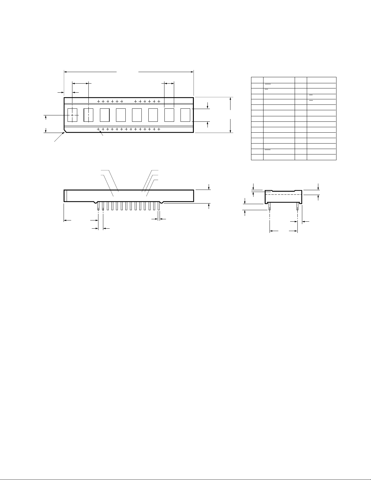
Package Dimensions
SYM.
TYP.
TYP. (NON-ACCUM)
LUMINOUS INTENSITY CATEGORY
COLOR BIN (NOTE 3)
COUNTRY OF ORIGIN
2.08
(0.082)
IMAGE PLANE
(FOR REFERENCE ONLY)
2.01 (0.79)
6.60
(0.260)
9.70
(0.382)
6.96
(0.274)
[4]
3.91
(0.154)
SYM.
19.01
(0.749)
2.54 ± 0.13
(0.100 ± 0.005)
TYP.
DIA.
0.51 ± 0.13
(0.200 ± 0.005)
PART NUMBER
15.24
(0.600)
0.38
(0.015)
PIN # FUNCTION PIN # FUNCTION
1
2
3
4
5
6
7
8
9
10
11
12
13
14
RST
FL
A
0
A
1
A
2
A
3
DO NOT CONNECT
DO NOT CONNECT
DO NOT CONNECT
A
4
CLS
CLK
WR
V
DD
15
16
17
18
19
20
21
22
23
24
25
26
27
28
GND (SUPPLY)
GND (LOGIC)
CE
RD
D
0
D
1
NO PIN
NO PIN
D
2
D
3
D
4
D
5
D
6
D
7
PIN FUNCTION ASSIGNMENT TABLE
3 4 5
6
7
19.41
(0.764)
4.51
(0.178)
70.87 (2.790)
TYP.
8.84
(0.348)
TYP.
PIN 1 IDENTIFIER
PIN DESIGNATION
NOTES:
1. DIMENSIONS ARE IN mm (INCHES).
2. UNLESS OTHERWISE SPECIFIED, TOLERANCE ON ALL DIMENSIONS IS ± 0.25 mm (0.010 INCH).
3. FOR YELLOW AND GREEN DEVICES ONLY.
HDSP-250X Y Z
YYWW COO
DATE CODE
2
1
1
28
0
TYP.
5.08
(0.200)
3
Page 4
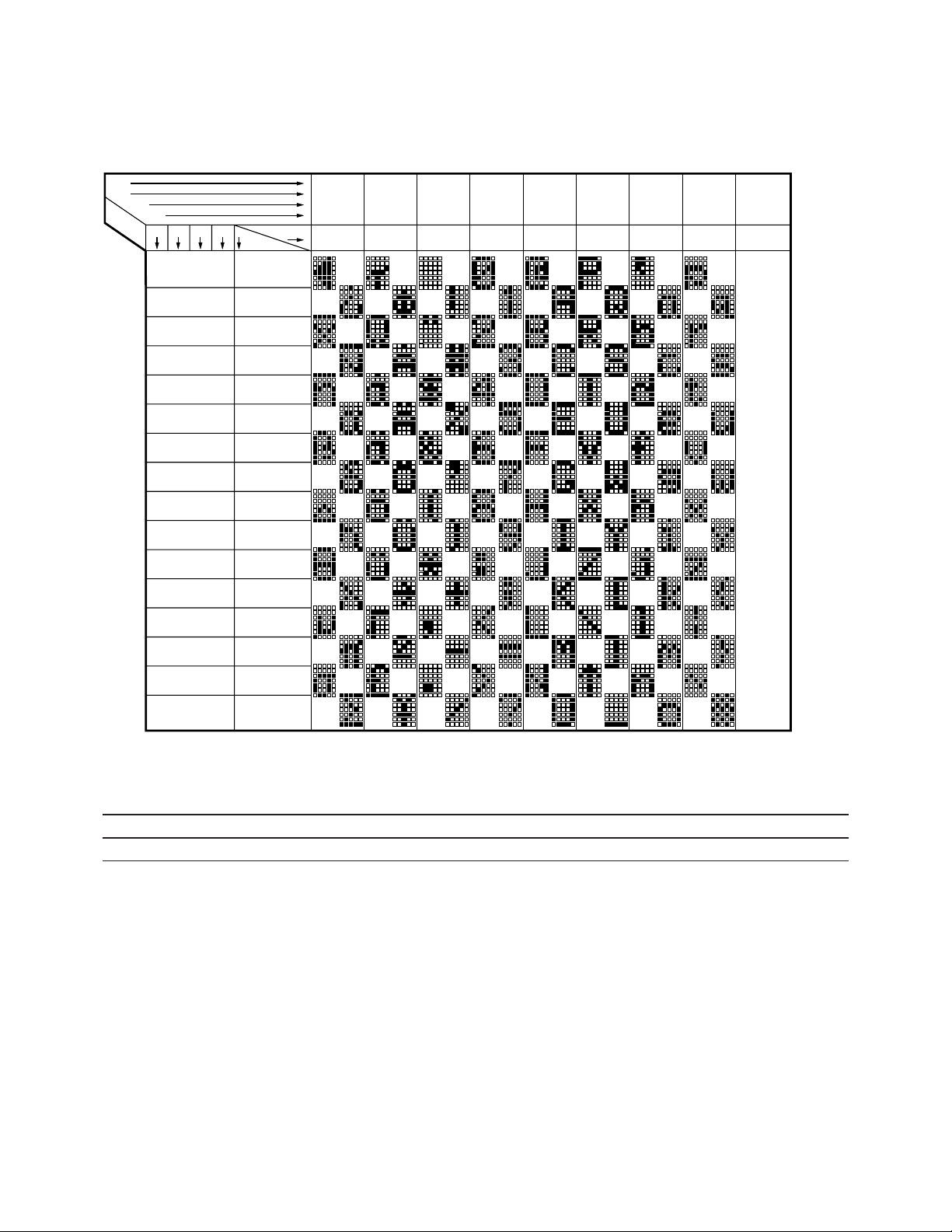
ASCII Character Set HDSP-210X, HDSP-211X, HDSP-250X Series
D7
D6
D5
D4
BITS
D3 D0D2 D1
ROW
COLUMN
0000 0
0001 1
0010 2
0011 3
0100 4
0101 5
0110 6
0111 7
1000 8
1001 9
1010 A
1011 B
1100 C
1101 D
1110 E
1111 F
0
0
0
0
0
0
0
0
1
1
0
0
1
0
2
0
0
1
1
3
0
1
0
0
4
0
1
0
1
5
0
1
1
0
6
0
1
1
1
7
1
X
X
X
8–F
16
U
S
E
R
D
E
F
I
N
E
D
C
H
A
R
A
C
T
E
R
S
Recommended Operating Conditions
Parameter Symbol Minimum Nominal Maximum Units
Supply Voltage VDD 4.5 5.0 5.5 V
4
Page 5

Electrical Characteristics Over Operating Temperature Range (-45°C to +85°C)
4.5 V < VDD < 5.5 V, unless otherwise specied
TA = 25°C -45°C < TA < + 85°C
VDD = 5.0 4.5 V < VDD < 5.5 V
Parameter Symbol Typ. Max. Min. Max. Units Test Conditions
Input Leakage IIH 1.0 µA VIN = 0 to VDD,
(Input without pullup) IIL -1.0 pins CLK, D0-D
A0-A
Input Current I
-11 -18 -30 µA VIN = 0 to VDD,
IPL
(Input with pullup) pins CLS, RST,
WR, RD, CE, FL
IDD Blank I
(BLK) 0.5 3.0 4.0 mA VIN = V
DD
IDD 8 digits IDD(V) 200 255 330 mA “V” on in all 8
12 dots/character
[1,2]
locations
IDD 8 digits IDD(#) 300 370 430 mA “#” on in al
20 dots/character
[1,2,3,4]
Input Voltage High VIH 2.0 VDD V
+0.3
Input Voltage Low VIL GND 0.8 V
-0.3 V
Output Voltage High VOH 2.4 V VDD = 4.5 V,
IOH = -40 µA
Output Voltage Low VOL 0.4 V VDD = 4.5 V,
D0-D
7
Output Voltage Low VOL 0.4 V VDD = 4.5 V,
CLK IOL = 40 µA
High Level Output IOH -60 mA VDD = 5.0 V
Current
Low Level Output IOL 50 mA VDD = 5.0 V
Current
Thermal Resistance Rq
15 °C/W
J-C
IC Junction-to-Case
4
DD
locations
IOL = 1.6 mA
Notes:
1. Average IDD measured at full brightness. See Table 2 in Control Word Section for IDD at lower brightness levels. Peak IDD = 28/15 x IDD (#).
2. Maximum IDD occurs at -55°C.
3. Maximum IDD(#) = 355 mA at VDD = 5.25 V and IC TJ = 150°C.
4. Maximum IDD(#) = 375 mA at VDD = 5.5 V and IC TJ = 150°C.
5
Page 6

Optical Characteristics at 25°C
[1]
VDD = 5.0 V at Full Brightness
Luminous Intensity Peak Dominant
Character Average (#) Wavelength Wavelength
Part Iv (mcd) l
ld
Peak
Description Number Min. Typ. (nm) (nm)
AlGaAs HDSP-2107 8.0 15.0 645 637
-2504
HER HDSP-2112 2.5 7.5 635 626
-2502
Orange HDSP-2110 2.5 7.5 600 602
-2500
Yellow HDSP-2111 2.5 7.5 583 585
-2501
High Performance HDSP-2113 2.5 7.5 568 574
Green -2503
Note:
1. Refers to the initial case temperature of the device immediately prior to measurement.
AC Timing Characteristics Over Temperature Range (-45°C to +85°C)
4.5 V < V
< 5.5 V, unless otherwise specied
DD
Reference
Number Symbol Description Min.
1 t
Write 210
Read 230 ns
2 t
3 tCE Chip Enable Active Time
Write 140
Read 160 ns
4 t
5 t
6 t
Write 140
Read 160 ns
7 t
Read/Write Signal
8 tW Write Active Time 100 ns
9 t
10 tWH Data Write Hold Time 20 ns
11 tR Chip Enable Active Prior to Valid Data 160 ns
12 tRD Read Active Prior to Valid Data 75 ns
13 tDF Read Data Float Delay 10 ns
tRC Reset Active Time
Display Access Time
ACC
Address Setup Time to Chip Enable 10 ns
ACS
[2,3]
Address Hold Time to Chip Enable 20 ns
ACH
Chip Enable Recovery Time 60 ns
CER
Chip Enable Active Prior to Rising Edge of
CES
Chip Enable Hold Time to Rising Edge of
CEH
Data Write Setup Time 50 ns
WSU
[2,3]
0 ns
[4]
300 ns
[2,3]
[1]
Units
Notes:
1. Worst case values occur at an IC junction temperature of 150°C.
2. For designers who do not need to read from the display, the Read line can be tied to VDD and the Write and Chip Enable lines can be tied together.
3. Changing the logic levels of the Address lines when CE = “0” may cause erroneous data to be entered into the Character RAM, regardless of
the logic levels of the WR and RD lines.
4. The display must not be accessed until after 3 clock pulses (110 µs min. using the internal refresh clock) after the rising edge of the reset line.
6
Page 7

AC Timing Characteristics Over Temperature Range (-45°C to +85°C)
1
9
8
6
32
CE
7
10
4 2
5
A0 -A
4
FL
D0 -D
7
WR
INPUT PULSE LEVELS: 0.6 V to 2.4 V
4.5 V < V
Symbol Description 25°C Typ. Min.
F
OSC
[2]
F
RF
[3]
F
FL
[4]
t
ST
Notes:
1. Worst case values occur at an IC junction temperature of 150°C.
2. FRF = F
3. FFL = F
4. tST = 262,144/F
< 5.5 V, unless otherwise specied
DD
[1]
Units
Oscillator Frequency 57 28 kHz
Display Refresh Rate 256 128 Hz
Character Flash Rate 2 1 Hz
Self Test Cycle Time 4.6 9.2 sec
/224.
OSC
/28,672.
OSC
OSC
.
Write Cycle Timing Diagram
7
Page 8

Read Cycle Timing Diagram
1
12
11
6
3
2
CE
7
13
4 2
5
A0 -A
4
FL
D0 -D
7
RD
INPUT PULSE LEVELS: 0.6 V to 2.4 V
OUTPUT REFERENCE LEVELS: 0.6 V to 2.2 V
OUTPUT LOADING = 1 TTL LOAD AND 100 pF
RELATIVE LUMINOUS INTENSITY
(NORMALIZED TO 1 AT 25°C)
-55
0
TA – AMBIENT TEMPERATURE – °C
65
-35
45 85
3.5
3.0
2.5
1.5
1.0
0.5
5 25-15
2.0
-45
HER HDSP-2112/2502
ORANGE HDSP-2110/2500
YELLOW HDSP-2111/2501
GREEN
HDSP-2113/2503
Relative Luminous Intensity vs. Temperature
8
Page 9

Electrical Description
Pin Function Description
RESET (RST, pin 1) Initializes the display.
FLASH (FL, pin 2) FL low indicates an access to the Flash RAM and is unaffected by the
state of address lines A3-A4.
ADDRESS INPUTS Each location in memory has a distinc t address. Address inputs (A0-A2)
(A0-A4, pins 3-6, 10) select a spec ific location in the Characte r RAM , the Flas h RAM or a
particular row in the UDC (User-Defined Character) RAM. A3-A4 are used
to sel ect w hich secti on o f memory is a ccess ed. Tabl e 1 sh ows the
logic levels needed to access each section of memory.
Table 1. Logic Levels to Access Memory
Section of Memory FL A4 A3 A2 A1 A
Flash RAM 0 X X Char. Address
UDC Address Register 1 0 0 Don’t Care
UDC RAM 1 0 1 Row Address
Control Word Register 1 1 0 Don’t Care
Character RAM 1 1 1 Character Address
CLOCK SELECT Used to select either an internal (CLS = 1) or external (CLS = 0) clock source.
(CLS, pin 11)
0
CLOCK INPUT/OUTPUT Outputs the master clock (CLS = 1) or inputs a clock (CLS = 0) for slave displays.
(CLK, pin 12)
WRITE (WR, pin 13) Data is written into the display when the WR input is low and the CE input is low.
CHIP ENABLE (CE, pin 17) Must be at a logic low to read or write data to the display and must go high between
each read and write cycle.
READ (RD, pin 18) Data is read from the display when the RD input is low and the CE input is low.
DATA Bus (D0-D7, Used to read from or write to the display.
pins 19, 20, 23-28)
GND (SUPPLY ) (pin 15) Analog ground for the LED drivers.
GND (LOGIC) (pin 16) Digital ground for internal logic.
VDD (POWER) (pin 14) Positive power supply input.
9
Page 10

A3A
4
FL
EN
UDC ADDR REGISTER
UDC
ADDR
RDWRD
0
-D
7
CLR
PRE SET
CE
A3A
4
A
0
-A
2
0
-D
7
FL
CE
WR
RD
A3A
4
FL
CE
FL
CE
A3A
4
FL
CE
A3A
4
FL
CE
EN
8 x 8
CHARACTER
RAM
D
0
-D
6
RDWRD
0
-D
7
A
0
-A
2
RESET
CHAR ADDR
D
7
EN
FLASH
RAM
FLASH
DATA
RDWRD0A
0
-A
2
RESET
CHAR ADDR
EN
UDC RAM
DOT
DATA
RDWRD
0
-D
4
D
0
-D
4
A
0
-A
2
UDC ADDR
ROW SET
EN
EN
ROW
SEL
SELF
TEST
ASCII
DECODER
DOT
DATA
D
0
-D
6
TIMING
TIMING
DOT
DRIVERS
DOT
DATA
EN
FLASH
CONTROL WORD
REGISTER
0
1
RD
WR
RST
CLK
OCS
CLS
CLR1
CLR2
D
0
-D
7
RESET
SELF TEST
RESULT
234
6
7
SELF
TEST
IN
SELF TEST
SELF TEST
SELF
TEST
START
8 5x7
LED
CHARACTERS
ROW DRIVERS
VISUAL
TEST
ROM
TEST
CLR
TEST OK
TEST OK
INTENSITY
INTENSITY
FLASH
FLASH
BLINK
BLINK
RESET
RESET
CLOCK
TIMING
AND
CONTROL
CHAR
ADDR
ROW SET
TIMING
Figure 1. HDSP-210X/-211X/-212X/-250X internal block diagram.
10
Page 11

Display Internal Block Diagram
CE
FL A4A3A2A1A
0
RST WR RD
CHARACTER
ADDRESS
SYMBOL IS ACCESSED IN LOCATION
SPECIFIED BY THE CHARACTER ADDRESS ABOVE
01
0 0
0 1
1
1 11
0
1 1
UNDEFINED
CONTROL SIGNALS
CHARACTER RAM ADDRESS
CHARACTER RAM DATA FORMAT
WRITE TO DISPLAY
READ FROM DISPLAY
UNDEFINED
000 = LEFT MOST
111 = RIGHT MOST
D7D6D5D4D3D2D1D
0
0
128 ASCII CODE
X X X UDC CODE1
DISPLAY
0 = LOGIC 0; 1 = LOGIC 1; X = DO NOT CARE
DIG0DIG1DIG2DIG3DIG4DIG5DIG6DIG
7
001 010 011 100 101 110 111000
Figure 1 shows the internal block diagram of the HDSP210X/-211X/-250X displays. The CMOS IC consists of an 8
byte Character RAM, an 8 bit Flash RAM, a 128 character
ASCII decoder, a 16 character UDC RAM, a UDC Address
Character RAM This RAM stores either ASCII character data or a UDC RAM address.
Flash RAM This is a 1 x 8 RAM which stores Flash data.
User-Dened Character RAM This RAM stores the dot pattern for custom characters.
(UDC RAM)
User-Dened Character This register is used to provide the address to the UDC RAM when the user is
Address Register writing or reading a custom character.
(UDC Address Register)
Control Word Register This register allows the user to adjust the display brightness, ash individual
characters, blink, self test, or clear the display.
Register, a Control Word Register, and refresh circuitry
necessary to synchronize the decoding and driving of
eight 5 x 7 dot matrix characters. The major user-accessible portions of the display are listed below:
Character RAM
Figure 2 shows the logic levels needed to access the
HDSP-210X/-211X/-250X Character RAM. During a
normal access, the CE = “0” and either RD = “0” or WR =
“0.” However, erroneous data may be written into the
Character RAM if the address lines are unstable when CE
= “0” regardless of the logic levels of the RD or WR lines.
Address lines A0-A2 are used to select the location in the
Character RAM. Two types of data can be stored in each
Character RAM location: an ASCII code or a UDC RAM
address. Data bit D7 is used to dierentiate between the
ASCII character and a UDC RAM address. D7 = 0 enables
the ASCII decoder and D7 = 1 enables the UDC RAM. D0D6 are used to input ASCII data and D0-D3 are used to
input a UDC address.
11
Figure 2. Logic levels to access the character RAM.
Page 12

UDC RAM and UDC Address Register
CE
FL A4A3A2A1A
0
RST WR RD
01
0 0
0 1
1
0 01 X X X
0
1 1
UNDEFINED
CONTROL SIGNALS
UDC ADDRESS REGISTER ADDRESS
UDC ADDRESS REGISTER DATA FORMAT
WRITE TO DISPLAY
READ FROM DISPLAY
UNDEFINED
000 = ROW 1
110 = ROW 7
D7D6D5D4D3D2D1D
0
X UDC CODE
X X X
FL A4A3A2A1A
0
0 11 ROW SELECT
UDC RAM ADDRESS
UDC RAM C C
DATA FORMAT O O
L L
1 5
0 = LOGIC 0; 1 = LOGIC 1; X = DO NOT CARE
D7D6D5D4D3D2D1D
0
X DOT DATA
X X
CERST WR RD
01
0 0
0 1
1 0
1 1
UNDEFINED
CONTROL SIGNALS
WRITE TO DISPLAY
READ FROM DISPLAY
UNDEFINED
C C C C C
O O O O O
L L L L L
1 2 3 4 5
D4D3D2D1D
0
UDC CHARACTER HEX CODE
1 1 1 1 1 ROW 1 • • • • • 1F
1 0 0 0 0 ROW 2 • 10
1 0 0 0 0 ROW 3 • 10
1 1 1 1 0 ROW 4 • • • • 1D
1 0 0 0 0 ROW 5 • 10
1 0 0 0 0 ROW 6 • 10
1 0 0 0 0 ROW 7 • 10
IGNORED
0 = LOGIC 0; 1 = LOGIC 1; * = ILLUMINATED LED
Figure 3 shows the logic levels needed to access the UDC
RAM and the UDC Address Register. The UDC Address
Register is eight bits wide. The lower four bits (D0-D3) are
used to select one of the 16 UDC locations. The upper
four bits (D4-D7) are not used. Once the UDC address has
been stored in the UDC Address Register, the UDC RAM
can be accessed.
To completely specify a 5 x 7 character, eight write cycles
are required. One cycle is used to store the UDC RAM
address in the UDC Address Register and seven cycles are
used to store dot data in the UDC RAM. Data is entered by
rows and one cycle is needed to access each row. Figure 4
shows the organization of a UDC character assuming the
symbol to be stored is an “F.” A0-A2 are used to select the
row to be accessed and D0-D4 are used to transmit the
row dot data. The upper three bits (D5-D7) are ignored.
D0 (least signicant bit) corresponds to the right most
column of the 5 x 7 matrix and D4 (most signicant bit)
corresponds to the left most column of the 5 x 7 matrix.
Flash RAM
Figure 5 shows the logic levels needed to access the
Flash RAM. The Flash RAM has one bit associated with
each location of the Character RAM. The Flash input is
used to select the Flash RAM while address lines A3-A4
are ignored. Address lines A0-A2 are used to select the
location in the Flash RAM to store the attribute. D0 is used
to store or remove the ash attribute. D0 = “1” stores the
attribute and D0 = “0” removes the attribute.
When the attribute is enabled through bit 3 of the
Control Word and a “1” is stored in the Flash RAM, the
corresponding character will ash at approximately 2
Hz. The actual rate is dependent on the clock frequency.
For an external clock the ash rate can be calculated by
dividing the clock frequency by 28,672.
Figure 3. Logic levels to access a UDC character.
12
Figure 4. Data to load “”F’’ into the UDC RAM.
Page 13

CE
FL A4A3A2A1A
0
RST WR RD
01
0 0
0 1
1
X X0
0
1 1
UNDEFINED
REMOVE FLASH AT
SPECIFIED DIGIT LOCATION
STORE FLASH AT
SPECIFIED DIGIT LOCATION
CONTROL SIGNALS
FLASH RAM ADDRESS
FLASH RAM DATA FORMAT
0 = LOGIC 0; 1 = LOGIC 1; X = DO NOT CARE
WRITE TO DISPLAY
READ FROM DISPLAY
UNDEFINED
D7D6D5D4D3D2D1D
0
X
X X X X X X
0
1
CHARACTER
ADDRESS
000 = LEFT MOST
111 = RIGHT MOST
CE
FL A4A3A2A1A
0
RST WR RD
01
0 0
0 1
1
1 0 X X X1
0
1 1
UNDEFINED
CONTROL SIGNALS
CONTROL WORD ADDRESS
CONTROL WORD DATA FORMAT
0 = LOGIC 0; 1 = LOGIC 1; X = DO NOT CARE
0 DISABLE FLASH
1 ENABLE FLASH
BRIGHTNESS
CONTROL
LEVELS
0 DISABLE BLINKING
1 ENABLE BLINKING
0 NORMAL OPERATION
1 CLEAR FLASH AND CHARACTER RAMS
0 X NORMAL OPERATION; X IS IGNORED
1 X START SELF TEST; RESULT GIVEN IN X
X = 0 FAILED X = 1 PASSED
WRITE TO DISPLAY
READ FROM DISPLAY
UNDEFINED
D7D6D5D4D3D2D1D
0
C
S S BL F B
0 0 0 100%
0 0 1 80%
0 1 0 53%
0 1 1 40%
1 0 0 27%
1 0 1 20%
1 1 0 13%
1 1 1 0%
B B
Control Word Register
Figure 6 shows how to access the Control Word Register.
This 8-bit register performs ve functions: Brightness
control, Flash RAM control, Blinking, Self Test, and Clear.
Each function is independent of the others; however, all
bits are updated during each Control Word write cycle.
Brightness (Bits 0-2)
Bits 0-2 of the Control Word adjust the brightness of the
display. Bits 0-2 are interpreted as a three bit binary code
with code (000) corresponding to maximum brightness
and code (111) corresponding to a blanked display. In
addition to varying the display brightness, bits 0-2 also
vary the average value of IDD. IDD can be calculated at any
brightness level by multiplying the percent brightness
level by the value of IDD at the 100% brightness level.
These values of IDD are shown in Table 2.
Flash Function (Bit 3)
Bit 3 determines whether the ashing character attribute
is on or o. When bit 3 is a“1,” the output of the Flash RAM
is checked. If the content of a location in the Flash RAM is
a “1,” the associated digit will ash at approximately 2 Hz.
For an external clock, the blink rate can be calculated by
driving the clock frequency by 28,672. If the ash enable
bit of the Control Word is a “0,” the content of the Flash
RAM is ignored. To use this function with multiple display
systems, see the Display Reset section.
Blink Function (Bit 4)
Bit 4 of the Control Word is used to synchronize blinking
of all eight digits of the display. When this bit is a “1” all
eight digits of the display will blink at approximately 2
Hz. The actual rate is dependent on the clock frequency.
For an external clock, the blink rate can be calculated by
dividing the clock frequency by 28,672. This function will
override the Flash function when it is active. To use this
function with multiple display systems, see the Display
Reset section.
Figure 5. Logic levels to access the ash RAM.
Table 2. Current Requirements at Dierent Brightness Levels VDD = 5.0 V
% Current at 25°C
Symbol D2 D1 D0 Brightness Typ. Units
IDD (V) 0 0 0 100 200 mA
0 0 1 80 160 mA
0 1 0 53 106 mA
0 1 1 40 80 mA
1 0 0 27 54 mA
1 0 1 20 40 mA
1 1 0 13 26 mA
13
Figure 6. Logic levels to access the control word register
Page 14

CERST WR RD
0 = LOGIC 0; 1 = LOGIC 1; X = DO NOT CARE
NOTE:
IF RST, CE, AND WR ARE LOW, UNKNOWN
DATA MAY BE WRITTEN INTO THE DISPLAY.
FL
0
1 X X X X X
A4 -A0D7 -D
0
Self Test Function (Bits 5, 6)
Bit 6 of the Control Word Register is used to initiate the
self test function. Results of the internal self test are
stored in bit 5 of the Control Word. Bit 5 is a read only bit
where bit 5 = “1” indicates a passed self test and bit 5 =
“0” indicates a failed self test.
Setting bit 6 to a logic 1 will start the self test function.
The built-in self test function of the IC consists of two
internal routines which exercise major portions of the
IC and illuminate all of the LEDs. The rst routine cycles
the ASCII decoder ROM through all states and performs
a checksum on the output. If the checksum agrees
with the correct value, bit 5 is set to “1.” The second
routine provides a visual test of the LEDs using the drive
circuitry. This is accomplished by writing checkered and
inverse checkered patterns to the display. Each pattern is
displayed for approximately 2 seconds.
During the self test function the display must not be
accessed. The time needed to execute the self test
function is calculated by multiplying the clock period
by 262,144. For example, assume a clock frequency of
58 KHz, then the time to execute the self test function
frequency is equal to (262,144/58,000) = 4.5 second
duration.
At the end of the self test function, the Character RAM
is loaded with blanks, the Control Word Register is set to
zeros except for bit 5, the Flash RAM is cleared, and the
UDC Address Register is set to all ones.
Clear Function (Bit 7)
Bit 7 of the Control Word will clear the Character RAM
and the Flash RAM. Setting bit 7 to a “1” will start the
clear function. Three clock cycles (110 ms minimum using
the internal refresh clock) are required to complete the
clear function. The display must not be accessed while
the display is being cleared. When the clear function
has been completed, bit 7 will be reset to a “0.” The ASCII
character code for a space (20H) will be loaded into the
Character RAM to blank the display and the Flash RAM
will be loaded with “0”s. The UDC RAM, UDC Address
Register, and the remainder of the Control Word are
unaected.
Figure 7. Logic levels to reset the display.
Display Reset
Figure 7 shows the logic levels needed to Reset the
display. The display should be Reset on Power-up. The
external Reset clears the Character RAM, Flash RAM,
Control Word and resets the internal counters. After the
rising edge of the Reset signal, three clock cycles (110 µs
minimum using the internal refresh clock) are required
to complete the reset sequence. The display must not
be accessed while the display is being reset. The ASCII
Character code for a space (20H) will be loaded into
the Character RAM to blank the display. The Flash RAM
and Control Word Register are loaded with all “0”s. The
UDC RAM and UDC Address Register are unaected. All
displays which operate with the same clock source must
be simultaneously reset to synchronize the Flashing and
Blinking functions.
Mechanical and Electrical Considerations
The HDSP-210X/-211X/-250X are 28 pin dual-in-line
packages with 26 external pins. The devices can be
stacked horizontally and vertically to create arrays of any
size. The HDSP-210X/-211X/-250X are designed to operate
continuously from -45°C to +85°C with a maximum of 20
dots on per character at 5.25 V. Illuminating all thirty-ve
dots at full brightness is not recommended.
The HDSP-210X/-211X/-250X are assembled by die
attaching and wire bonding 280 LED chips and a CMOS
IC to a thermally conductive printed circuit board. A polycarbonate lens is placed over the PC board creating an air
gap over the LED wire bonds. A protective cap creates an
air gap over the CMOS IC. Backll epoxy environmentally
seals the display package. This package construction
makes the display highly tolerant to temperature cycling
and allows wave soldering.
The inputs to the IC are protected against static discharge
and input current latchup. However, for best results
standard CMOS handling precautions should be used.
Prior to use, the HDSP-210X/-211X/-250X should be
stored in antistatic tubes or in conductive material.
During assembly, a grounded conductive work area
should be used, and assembly personnel should wear
conductive wrist straps. Lab coats made of synthetic
material should be avoided since they are prone to static
buildup. Input current latchup is caused when the CMOS
inputs are subjected to either a voltage below ground
(VIN < ground) or to a voltage higher than VDD (VIN >
VDD) and when a high current is forced into the input. To
prevent input current latchup and ESD damage, unused
inputs should be connected either to ground or to VDD.
Voltages should not be applied to the inputs until VDD
has been applied to the display.
14
Page 15

Thermal Considerations
The HDSP-210X/-211X/-212X/250X have been designed
to provide a low thermal resistance path for the CMOS
IC to the 26 package pins. Heat is typically conducted
through the traces of the printed circuit board to free
air. For most applications no additional heatsinking is
required.
Measurements were made on a 32 character display
string to determine the thermal resistance of the display
assembly. Several display boards were constructed using
0.062 in. thick printed circuit material, and one ounce
copper 0.020 in. traces. Some of the device pins were
connected to a heatsink formed by etching a copper
area on the printed circuit board surrounding the display.
A maximally metallized printed circuit board was also
evaluated. The junction temperature was measured for
displays soldered directly to these PC boards, displays
installed in sockets, and nally displays installed in
sockets with a lter over the display to restrict airow. The
results of these thermal resistance measurements, Rq
are shown in Table 3 and include the eects of Rq
J-C
J-A
.
Ground Connections
Two ground pins are provided to keep the internal IC
logic ground clean. The designer can, when necessary,
route the analog ground for the LED drivers separately
from the logic ground until an appropriate ground
plane is available. On long interconnections between
the display and the host system, the designer can keep
voltage drops on the analog ground from aecting the
display logic levels by isolating the two grounds.
Soldering and Post Solder
Cleaning Instructions for the
HDSP-210X/-211X/-250X
The HDSP-210X/-211X/-250X may be hand soldered or
wave soldered with SN63 solder. When hand soldering,
it is recommended that an electronically temperature
controlled and securely grounded soldering iron be used.
For best results, the iron tip temperature should be set at
315°C (600°F). For wave soldering, a rosin-based RMA ux
can be used. The solder wave temperature should be set
at 245°C ± 5°C (473°F ± 9°F), and the dwell in the wave
should be set between 11 /2 to 3 seconds for optimum
soldering. The preheat temperature should not exceed
105°C (221°F) as measured on the solder side of the PC
board.
For additional information on soldering and post solder
cleaning, see Application Note 1027, Soldering LED Com-
ponents.
Contrast Enhancement
The objective of contrast enhancement is to provide
good readability in a variety of ambient lighting conditions. For information on contrast enhancement see
Application Note 1015, Contrast Enhancement Techniques
for LED Displays.
The logic ground should be connected to the same
ground potential as the logic interface circuitry.
The analog ground and the logic ground should be
connected at a common ground which can withstand
the current introduced by the switching LED drivers.
When separate ground connections are used, the analog
ground can vary from -0.3 V to +0.3 V with respect to the
logic ground. Voltage below -0.3 V can cause all dots to
be on. Voltage above +0.3 V can cause dimming and dot
mismatch.
Table 3. Thermal Resistance, qJA, Using Various Amounts
of Heatsinking Material
Heatsinking
Metal W/Sockets W/O Sockets W/Sockets
per Device W/O Filter W/O Filter W/Filter
sq. in. (Avg.) (Avg.) (Avg.) Units
0 31 30 35 °C/W
1 31 28 33 °C/W
3 30 26 33 °C/W
Max. Metal 29 25 32 °C/W
4 Board Avg 30 27 33 °C/W
Page 16

Intensity Bin Limits for HDSP-2107
Intensity Range (mcd)
Bin Min. Max.
I 5.12 9.01
J 7.68 13.52
K 11.52 20.28
L 17.27 30.42
M 25.39 45.63
Note:
Test conditions as specied in Optical Characteristic table.
Intensity Bin Limits for HDSP-211x
and HDSP-250x (Except HDSP-2504)
Intensity Range (mcd)
Bin Min. Max.
G 2.50 4.00
H 3.41 6.01
I 5.12 9.01
J 7.68 13.52
K 11.52 20.28
Color Bin Limits
Color Range (nm)
Color Bin Min. Max.
Yellow 3 581.5 585.0
4 584.0 587.5
5 586.5 590.0
6 589.0 592.5
7 591.5 595.0
Green 1 576.0 580.0
2 573.0 577.0
3 570.0 574.0
4 567.0 571.5
Note:
Test conditions as specied in Optical Characteristic table.
Note:
Test conditions as specied in Optical Characteristic table.
Intensity Bin Limit for HDSP-2504
Intensity Range (mcd)
Bin
J 7.68 13.52
K 11.52 20.28
L 17.27 30.42
M 25.91 45.63
Note:
Test conditions as specied in Optical Characteristic table.
Min. Max
For product information and a complete list of distributors, please go to our website: www.avagotech.com
Avago, Avago Technologies, and the A logo are trademarks of Avago Technologies Limited in the United States and other countries.
Data subject to change. Copyright © 2005-2008 Avago Technologies Limited. All rights reserved. Obsoletes 5989-3183EN
AV02-0629EN - May 9, 2008
 Loading...