

Page 1

Fibre Channel Transmitter and
Receiver Chipset
Technical Data
HDMP-1512 Transmitter
HDMP-1514 Receiver
Features
• ANSI X3.230-1994 Fibre
Channel Standard
Compatible (FC-0)
• Selectable 531.25 Mbaud or
1062.5 Mbaud Data Rates
• Selectable On Chip Laser
Driver and 50 Ω Cable
Driver
• TTL Compatible I/Os
• Single +5.0 V Power Supply
Applications
• Mass Storage System I/O
Channel
• Work Station/Server I/O
Channel
• High Speed Peripheral
Interface
Description
The HDMP-1512 transmitter and
the HDMP-1514 receiver are
bipolar integrated circuits,
separately packaged, in 80 pin MQuad packages. They are used to
build a high speed Fibre Channel
link for point to point data communications. Shown in Figure 1 is
a typical full duplex point-topoint Fibre Channel link. The
sending system provides parallel,
8B/10B, encoded data and a
transmit byte clock to the HDMP1512 transmitter. Using the transmit byte clock, the transmitter
converts the data to a serial
stream and sends it over a copper
cable or fiber-optic link. The
receiver converts the serial data
stream back to parallel encoded
data and presents it, along with
the recovered transmit byte
clock, to the receiving system.
The sending system has the
option to electrically wrap the
transmitted data back to the local
receiver. It is possible to transmit
over the cable driver, or laser
driver when data is being
wrapped back to the local
receiver.
The two-chip set (transmitter
chip and receiver chip) is
compatible with the FC-0 layer of
the American National Standards
Institute (ANSI), Fibre Channel
specification, X3.230-1994. This
specification defines four
standard rates of operation for
Fibre Channel links. The HDMP1512 and HDMP-1514 chip-set
will operate at the two highest
defined serial rates of 531.25
Mbaud and 1062.5 Mbaud. These
serial baud rates correspond to
8B/10B encoded byte rates of 50
Mbytes/sec and 100 Mbytes/sec
respectively. The proper setting
of a single pin on each chip
selects the desired rate of
operation.
Several features, exclusive to this
chip-set, make it ideal for use in
Fibre Channel links. In addition,
the laser driver on the transmitter
chip, the dual loss of light
detectors on the receiver chip,
and the power supervisor and
power reset features make this
chip-set ideal for use with laser
optics. The serial cable driver
(transmitter chip), and the cable
equalizer (on the receiver chip),
can be operated in conjunction
with, or as an alternative to, the
laser driver. The laser driver can
also be driven directly with an
external high speed serial input.
Altogether, the various features,
input/output options, and
flexibility of this chip-set make
several unique link configurations
possible. In particular, it is ideally
suited for use in applications
where conformance to the FCSI
specification # 301-Rev 1.0,
Gbaud Link Module Specification,
is desired.
656
5964-6637E (4/96)
Page 2

REF CLOCK
CLOCK
ENCODED DATA
ENCODED DATA
CLOCK
REF CLOCK
Figure 1. Point-to-Point Data Link.
DATA BYTE 0
Tx [00:09]
DATA BYTE 1
Tx [10:19]
Tx
Rx
10
10
SERIAL LINK
SERIAL LINK
-COMGEN
TTL INTERFACE
AND
INPUT LATCH
20
Rx
Tx
FRAME
MULTIPLEXER
± SI
SELECT
CLOCK
ENCODED DATA
ENCODED DATA
CLOCK
TS2
TS1
EWRAP
I/O
CABLE
DRIVERS
2
± LOUT
2
± SO
TBC
Figure 2. HDMP-1512 (Tx) Block Diagram.
Transmitter Operation
The block diagram of the HDMP1512 transmitter is shown in
Figure 2. The basic functions of
the transmitter chip are the TTL
Interface and Input Latch, Frame
Multiplexing, Input/Output
selection, cable drivers, Laser
Driver, and monolithic Phase
Locked loop clock generator. The
actual operation of each function
changes slightly, according to the
desired configuration and option
settings. Figures 18 and 19 show
schematically how to terminate
each pin on the HDMP-1512
when used in systems incorporating either copper or fiber media.
PLL/CLOCK
GENERATOR
PPSEL
SPDSEL
INTERNAL
CLOCKS
There are two main modes of
operation for the transmitter
chip, both are based on the
selected baud rate. The baud rate
is controlled by the appropriate
setting of the SPDSEL pin, #67.
When this pin is set low, the
transmitter operates at a serial
rate of 531.25 Mbaud. When pin
#67 is set high the transmitter
operates at a serial rate of 1062.5
Mbaud. As such, the two main
modes of operation are the
531.25 Mbaud mode and the
1062.5 Mbaud mode.
The transmitter does not encode
the applied data. It assumes the
2
LASER
DRIVER
-LZON
FAULT
± LZOUT
LASER
CONTROLS
data is pre-encoded using the
8B/10B encoding scheme as
defined in ANSI X3.230-1994.
The TTL input interface receives
data at the standard TTL levels
specified in the dc Electrical
Specification table. The internal
phase locked loop (PLL) locks to
the transmit byte clock, TBC.
TBC is supplied to the transmitter
chip by the sending system. TBC
should be a 53.125 MHz clock
(± 100 ppm) as defined in
X3.230-1994. Once the PLL has
locked to TBC, all the clocks used
by the transmitter are generated
by the internal clock generator.
657
Page 3

When operating in the 531.25
Mbaud mode, data byte 0,
Tx[00:09], is active and is
clocked into the input latch a
single byte (10 bits) on each
rising edge of TBC. In the 1062.5
Mbaud mode both data byte 0,
Tx[00:09], and data byte 1,
Tx[10:19], are active. In 1062.5
Mbaud mode, data byte 0 and
data byte 1 are clocked into the
transmitter on the rising edge of
every clock cycle, (TBC). There is
one minor variation possible in
the 1062.5 Mbaud mode, referred
to as “ping-pong” mode. Pingpong mode is selected by setting
the PPSEL pin (#34) high. In this
mode the transmitter clocks data
into the input latch one byte per
half clock cycle. Data byte 0 is
transmitted on the rising edge of
TBC and data byte 1 is transmitted 1/2 clock cycle later. See
Figure 16 for timing information.
The input latch will stop sending
the data applied to the Tx[00:09]
data pins when a low is applied to
the -COMGEN pin (#32) and will
send the pre-set special Fibre
Channel character, K28.5 instead.
The 8B/10B coding scheme,
adopted by Fibre Channel, converts 8 bit data words into 10 bit
representations of the actual
data. Of all the possible combina-
tions of 10 bit binary words, the
8B/10B code reserves 256 of
them to represent the valid
combinations of 8 bit data. Some
of the remaining combinations
are reserved for special functions.
The character reserved for
defining the transmitted word
boundary has been defined as the
K28.5 character, also known as a
comma character. The receiver
will automatically reset registers
and clock when it receives a
comma character (this will be
discussed in more detail in the
receiver operation section). Every
valid 8 bit data word is actually
represented by one of two 10 bit
codes, indicating either positive
or negative running disparity.
The input latch only generates
the K28.5 character with positive
disparity (0011111010).
In Figure 2, the Frame
Multiplexer utilizes shift registers
and a multi-stage multiplexing
scheme to convert the 10 or 20
parallel data bits to a serial data
stream. This serial data stream is
then fed directly into the Input/
Output Select portion of the
transmitter.
The I/O Select function allows use
of both the internally serialized
Fibre Channel data stream and an
externally supplied Fibre Channel
data stream denoted as ± SI (pins
11 and 12). By using the proper
settings of TS1, TS2, and EWRAP
(pins 76, 75, and 71
respectively), the internal data
stream and the external data
stream can be directed to various
combinations of the cable driver
output, the laser driver output,
and the electrical loopback
output. The possible I/O
combinations are listed in the
Input Output Select Table and the
functionality is described in more
detail in the Transmitter Laser
Driver Operation section below.
The cable driver function
provides a 50 Ω differential cable
driver output at pins 5 and 6
(± SO). The simplified circuit is
the O-BLL section shown in
Figure 10. A similar output is
provided to allow electrical
loopback, or wrap of the local
data back to the local receiver for
diagnostics. This is denoted as
± LOUT on pin 8 and pin 9.
The final function on the
transmitter chip is the Laser
Driver block which provides a
high speed differential output,
± LZOUT, at pins 19 and 20.
There are several other laser
control I/Os which will be
HDMP-1512 Input Output Select Table
Data Source For: Active Outputs
Mode TS1 TS2 EWRAP ±SO ±LZOUT ±LOUT ±SO ±LZOUT ±LOUT
0 0 0 0 NA Internal NA no yes no
1 0 0 1 NA NA Internal no no yes
2 0 1 0 Internal Internal NA yes yes no
3 0 1 1 Internal NA Internal yes no yes
4 1 0 0 Internal NA NA yes no no
5 1 0 1 NA Internal Internal no yes yes
6 1 1 0 Internal ± SI NA yes yes no
7 1 1 1 Internal NA ± SI yes no yes
658
Page 4

± SI
VCC_LZ1
VCC_LZ
GND_LZ
-LZON
LZPWRON
FAULT
INTERNAL
DATA
STREAM
11
12
16
23
24
25
26
30
36
29
INPUT
SELECT
MUX
LASER ON
ERROR
DETECTOR
AC AMP
DISABLE
WINDOW
DETECTOR
BANDGAP
REFERENCE
BANDGAP
DETECTOR
Tx CHIP BOUNDARY
+
AC AMP
–
LZDC
–
DC
OP-AMP
+
10 nF
10 nF
V
CC
17
+LZOUT
19
-LZOUT
20
LZCSE
14
21
_LZAC
0.1 µF
5 Ω
0.1 µF 0.1 µF
25 Ω TRANSMISSION LINE
POT 2
50 Ω
5 Ω
0.1 µF
0.1 µF
25 Ω
301 Ω
P1 (β >= 100)
8 Ω
25 Ω
V
CC
V
CC
P2
0.1 µF
2.2 Ω
EXTERNAL
CONTROL
-LZBG
V
CC
2715 28 22
LZTC
0.1 µF
POT 1 5 KΩ
Figure 3. Laser Driver Block Diagram and External Circuitry.
described in more detail in the
laser driver operation section
below.
± SI pins. The user selects
between these two data sources
through the proper settings of
pins TS1, TS2, and EWRAP (pins
Transmitter Laser Driver Operation
The block diagram of the HDMP1512, Tx, laser driver circuitry is
shown in Figure 3. The laser
driver is enabled by setting
-LZON (pin 30) low and
LZPWRON (pin 36) high. The
circuitry in Figure 3, shown
outside the chip boundary (dotted
box), illustrates the external
components required to complete
a typical laser driver connection.
76, 75, and 71). The possible
combinations of active inputs and
outputs are shown in the Input/
Output Select Table. The chosen
high speed input is then modulated onto the laser by the ac
amplifier. The external potentiometer, Pot 2, shown connected
to pin LZCSE (# 14) is used to
adjust the laser modulation
depth. The laser driver output is
at pins 19 and 20, ± LZOUT.
Laser diode dc bias control is
provided through the LZDC
The input data source to the laser
driver is user selected from either
the internally generated data
stream, or an externally supplied
high speed data stream. The
externally supplied data stream is
applied to the high speed input
(# 21) pin. Adjustment of Pot 1
sets the nominal dc bias desired
for the laser diode. The
equivalent output circuit of LZDC
is shown in Figure 4. Laser diode
fault and safety control is implemented through the combination
LZMDFLZBTP
VCC_LZ
54
400
LZDC
Figure 4. LZDC Equivalent Output
Circuit (Tx pin # 21).
of the window detector, error
detector, Laser On pin # 30
(-LZON), laser monitor diode
feedback pin # 22 (LZMDF), and
the op-amp dc bias control
circuit. The window detector
monitors the voltage on pin
LZMDF. If this voltage goes out
of range by more than ± 10%
from the nominal setting, the
659
Page 5

capacitor on pin LZTC (# 27) will
begin to discharge. After
approximately 2 msec, the
voltage on LZTC falls to the fault
value and the error detector will
bring the FAULT pin (# 29) high
to alert the system. The error
detector will also hold the voltage
on LZMDF low, until a reset is
initiated.
The -LZON pin is used to disable
the laser driver under system
control or in conjunction with an
external open-fiber control (OFC)
chip. This pin is also used to
reset the error detector and
recharge the capacitor on pin
LZTC.
The LZPWRON pin, # 36, is used
to hold off dc power to the laser
driver until proper dc bias is
applied to the laser diode. When
LZPWRON goes high, the laser
driver is enabled, when it is low,
it is disabled. If not used, this pin
should be tied low.
Receiver Operation
The block diagram of the HDMP1514 receiver is shown in Figure
5. The functions included on the
receiver are a coaxial cable
equalizer, two independent loss
of light (LOL) detectors, an input
select function, monolithic phase
locked loop and clock recovery
circuits, a clock generator, frame
demultiplexer and comma
detector, power supply supervisor, and output latch with TTL
drivers. Figures 20 and 21 show
schematically how to terminate
each pin on the HDMP-1514
when used in systems incorporating either copper or fiber media.
In the most basic sense, the
receiver accepts a serial electrical
data stream at 1062.5 Mbaud or
531.25 Mbaud and recovers the
8B/10B encoded parallel data and
clock that was applied to the
transmitter. Like the transmitter,
the receiver has several configuration options which interrelate
according to the desired mode of
operation.
The two main modes of operation
for the receiver are based on the
desired signalling rate. The
signalling rate is controlled by
the proper setting of the SPDSEL
pin # 71. When this pin is set
low, the receiver operates at a
serial rate of 531.25 Mbaud.
When pin # 71 is set high, the
receiver operates at a serial rate
of 1062.5 Mbaud.
In a typical configuration, the
serial electrical data stream will
be applied to the ± DI pins, # 19
and # 20 on the receiver. The
serial electrical data stream may
have been transmitted over a
fiber optic link or a copper cable
link (several variations of each
link type is possible). For use
with copper links, a selectable
cable equalizer is available at the
input. This equalizer can be
switched into or out of the data
LOLA
LOLB
EWRAP
DR_REF
± DI
-EQEN
± LIN
VCC_HS
Figure 5. HDMP-1514 (Receiver) Block Diagram.
CABLE
EQUALIZER
SUPERVISOR
SUPPLY
-POR
LOL
DETECTORS
INPUT
SELECT
PS_CT
660
L_UNUSE
PLL AND
CLOCK
SELECT
-LCK_REF
-TCLKSEL
FRAME
DEMUX
COMMA
DETECT
PPSEL
CLKIN
AND
INTERNAL
CLOCKS
EN_CDET
20
SPDSEL
CLOCK
GENERATOR
OUTPUT
LATCH AND
TTL
INTERFACE
10
10
RBC0
RBC1
COM_DET
DATA BYTE 0
Rx [00:09]
DATA BYTE 1
Rx [10:19]
Page 6

path using the -EQEN pin, # 32.
Setting pin #32 high disables the
equalizer. Setting pin # 32 low
enables the equalizer. The typical
performance of the input
equalizer is shown in the
(frequency response) plot of
Figure 7. The impact of the
equalizer is improved BER
performance over long lengths of
cable (10 to 20 meters).
Connected to the ± DI input pins,
prior to the equalizer, are the loss
of light detectors, LOLA (pin 28)
and LOLB (pin 29). Actually,
since these detectors monitor the
incoming serial electrical data
stream, they can be thought of as
loss of “signal” detectors. These
signals can be used to determine
if the incoming signal line is
connected properly. In the case
of a fiber optic system they can
be used to shut down laser output
power for laser safety considerations. The LOL detectors measure
transitions in the incoming data
stream that exceed a pre-set
peak-to-peak differential signal or
threshold level. The default peakto-peak differential threshold
voltage is 25 mV and can be
adjusted by connecting a resistive
divider to the DR_REF pin (#21)
as shown in Figure 6. The rela-
+5 V
2 KΩ
8 KΩ POTENTIOMETER
PIN #21,
DR_REF
2 KΩ
tionship of the DR_REF voltage
to the peak-to-peak differential
threshold voltage is shown in
Figure 8. When the input signal
level falls below the threshold
voltage for 4 clock cycles, or 80
bit times, the signals at pins 28
and 29 will go high.
Once the serial data stream
passes the cable equalizer
function it is directed to an Input
Select section. A second high
speed serial data input, denoted
± LIN, is applied at pins # 16 and
# 17 and is connected directly to
the Input Select section. This data
input is intended for diagnostic
purposes. It is not affected by the
cable equalizer and has no effect
on the loss of light detectors. The
± LIN input should mainly be
used when it is desired to directly
connect the local transmitter
serial output data stream to the
local receiver (local loopback).
The Input Select function uses
the EWRAP signal, pin # 34, to
determine which serial data
stream to pass on to the rest of
the receiver. If EWRAP is high,
then the ± LIN signal is used. If
EWRAP is low the ± DI signal is
used.
The PLL and Clock select
circuitry contains a monolithic,
tunable, oscillator. This oscillator
phase locks to the selected high
speed data input and recovers the
high speed serial clock. To keep
the internal oscillator tuned close
to the incoming signal frequency,
an external reference oscillator is
applied to the CLKIN input, pin
# 7. The signal on the -LCK_REF
input, pin # 36, controls whether
the receiver oscillator locks to the
reference oscillator or to the
incoming data stream. When
-LCK_REF is toggled low, the
receiver frequency locks to the
signal at CLKIN. When the
-LCK_REF pin is toggled high,
the receiver phase locks to the
selected high speed serial data
input. This process of locking to
a local reference oscillator, prior
to receiving incoming data,
improves (shortens) the overall
time required by the receiver to
acquire lock. The LUNUSE input,
pin 73 will cause the receiver to
frequency lock on the CLKIN
signal under faulty or no input
signal conditions. The LUNUSE
signal needs to be provided to the
receiver by an external open fiber
control circuit or other control
logic. Once the receiver has
locked to the incoming data
stream at ± DI (EWRAP = 0 and
-LCKREF = 1), if LUNUSE
toggles high then the receiver will
switch to frequency lock on
CLKIN. If, however, the receiver
is locked onto the local data
wrapped back to the ± LI input
(EWRAP = 1 and -LCKREF = 1)
then the receiver stays locked to
the incoming signal at ± LI even
when LUNUSE goes high. In
summary, when the LUNUSE
input is set low, the receiver
frequency locks to the CLKIN
signal when the input to
-LCKREF is low and phase locks
to either the ± DI or ± LI signal,
depending on which input is
selected, when -LCKREF toggles
high. LUNUSE then, is used to
cause the receiver to frequency
lock to the reference oscillator at
CLKIN after the receiver has
established phase lock to the
incoming data signal at ± DI, and
the system determines the link is
faulty and not in EWRAP mode.
Figure 6. Simple Circuit Used to
Adjust the Voltage on Rx pin # 21,
DR_REF.
661
Page 7

-LCK_REF EWRAP LUNUSE Rx Lock
0 x x CLKIN
100DI
1 0 1 CLKIN
111LI
110LI
The table above llustrates these
various settings.
incoming data stream at the ± DI
input but the actual frame or
word boundary will be undeterNormally, the recovered serial
clock is used by the clock generator to generate the various
internal clocks the receiver uses
including the receive clock
outputs RBC0 (pin 69) and RBC1
(pin 67).
mined. The EN_CDET pin (# 38)
should be set high now. With the
EN_CDET pin set high, the
receiver will scan the incoming
data stream for a comma charac-
ter. Once a comma character is
received, the internal clocks and
registers are reset giving proper
The final receiver clocking
feature is included for test
purposes only. By applying a low
to the -TCLKSEL input, pin 5, the
internal phase locked loop is
bypassed and the receiver uses
the CLKIN signal as the high
speed serial clock. Under normal
operating conditions the
-TCLKSEL pin should be tied
high.
frame alignment. The receiver
will reset on every comma
character that is transmitted as
long as EN_CDET is held high.
When the internal clock genera-
tor is reset due to the detection of
a comma character, internal
circuitry prevents a clock “sliver”
from appearing at the receive
clock outputs (RBC0 and RBC1).
This antisliver circuit assures
each clock output high, or low,
In a Fibre Channel link, frame
alignment is accomplished
through the transmission and
detection of the special character
K28.5, also known as a comma
character. Prior to actual data
transmission the system will
transmit a comma character over
the physical link. To start, the
receiver should be frequency
locked to the local reference
oscillator (-LCKREF set low). To
ensure frequency lock is
will be held for at least one half
the frame rate time. When
EN_CDET is set low the receiver
ignores all incoming comma
characters and assumes the
current frame and bit alignment
is correct. EN_CDET is
automatically disabled when
-LCKREF is set low. The
COM_DET pin, #75, on the
receiver will go high when a
comma character is detected (see
Figure 15).
achieved, -LCKREF should be
held low for a minimum of 500
µsec (see Rx Timing Characteristics, t
). It then should be
flock
toggled high. At this point the
receiver will phase lock to the
Now that frame alignment has
been achieved, the receiver is
ready to receive full speed serial
data and demultiplex it back to
its original 10 bit or 20 bit
4
2
0
-2
-4
-6
RELATIVE GAIN – dB
-8
-10
1.00E
1.00E
+ 06
Figure 7. Typical Frequency Response
Plot of the Internal Input Equalizer.
1.00E
+ 07
+ 08
FREQUENCY – f – Hz
1.00E
+ 09
1.00E
+ 10
parallel word format. This data is
then placed into the output latch.
The data output is presented in
the standard TTL output levels
and characteristics specified in
the dc and ac Electrical Specification tables. When operating in
531 Mbaud mode the receiver
generates output data in a single
byte wide (10 bits) output format.
This is data byte 0 and is denoted
RX[00:09] on pins 53 through
62. In 1063 Mbaud mode the data
output is generated in a two byte
wide (20 bits) format, data byte 0
and data byte 1. Data byte 0 is
denoted RX[00:09] on pins 53
through 62 and data byte 1 is
denoted RX[10:19] on pins 43
through 52. In standard operation
data byte 0 and data byte 1 will
both be clocked into the output
latch at the same time, on the
falling edge of RBC0. An
alternate mode of operation is
ping-pong mode. In ping-pong
mode the data is clocked out 1
byte at a time with byte 0 clocked
out on the falling edge of RBC0
and byte 1 clocked out on the
falling edge of RBC1. To set the
receiver to operate in ping-pong
mode, the PPSEL pin, # 76,
should be set high (otherwise it
should be tied low).
662
Page 8

Rx Power Supply Supervisor
A power supply supervisor feature
has been designed into the
receiver as a system aid during
power-up. The -POR (pin # 27)
output is held low until the power
supply voltage (VCC) crosses the
nominal threshold of 4.25 volts.
Then, following a delay time
determined by the capacitor value
connected to the PS_CT pin
(# 22), the -POR output goes high.
The typical delay time is 8 msec,
with a 0.47 µF capacitor attached
to PS_CT.
90
80
70
60
50
DEFAULT
40
THRESHOLD
30
20
p-p DIFFERENTIAL – mV
10
LOL THRESHOLD VOLTAGE –
0
0
0.5 2.5
DR_REF VOLTAGE – V
Figure 8. Typical Plot of Loss of Light
Threshold Voltage vs. DR_REF
Voltage.
1.0
1.5
2.0
Recommended Handling Precautions
Additional circuitry is built into the
various input and output pins on
these chips to protect them against
low level electrostatic discharge,
however, they are still ESD
sensitive and standard procedures
for static sensitive devices should
be used in the handling and
assembly of the HDMP-1512 and
the HDMP-1514. The packing
materials used for shipment of
these devices was selected to
provide ESD protection and to
prevent mechanical damage.
During test and use, under powerup conditions, extreme care should
be taken to prevent the high speed
I/Os from being connected to
ground as permanent damage to
the device is likely.
HDMP-1512 (Tx), HDMP-1514 (Rx)
Absolute Maximum Ratings
Operation in excess of any one of these conditions may result in permanent damage.
Symbol Parameter Units Min. Max.
V
V
IN,TTL
V
IN,H50
I
O,TTL
T
T
T
max
CC
stg
J
Supply Voltage V -0.5 6.0
TTL Input Voltage V -0.7 VCC + 0.7
I-H50 Input Voltage, Figure 9 V VCC - 2.0 VCC + 0.7
TTL Output Source Current mA 13
Storage Temperature °C -40 +130
Junction Operating Temperature °C 0 +130
Maximum Assembly Temperature (for 10 seconds °C 0 +260
maximum)
HDMP-1512 (Tx), HDMP-1514 (Rx)
Specified Operating Rates
TC = 0°C to +85°C, VCC = 4.5 V to 5.5 V
Transmit Byte Clock (TBC) Serial Baud Rate
(MHz) (MBaud/sec)
SPDSEL Min. Max. Min. Max.
0 52.0 54.0 520 540
1 52.0 54.0 1040 1080
663
Page 9
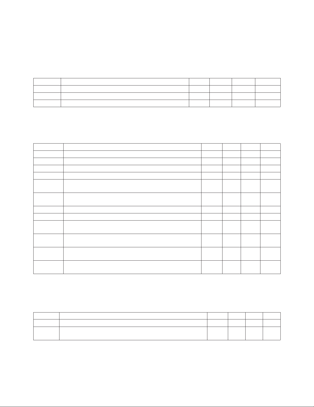
HDMP-1512 (Tx), HDMP-1514 (Rx)
Transmitter & Receiver Byte Rate Clock Requirements
TC = 0°C to +85°C, VCC = 4.5 V to 5.5 V
Symbol Parameter Unit Min. Typ. Max.
f Nominal Frequency MHz 53.120 53.125 53.130
F
tol
Frequency Tolerance (For Fibre Channel Compliance) ppm -100 +100
Symm Symmetry (Duty Cycle) % 40 60
HDMP-1512 (Tx), HDMP-1514 (Rx)
AC Electrical Specifications
TC = 0°C to +85°C, VCC = 4.5 V to 5.5 V, Unless Otherwise Specified
Symbol Parameter Units Min. Typ. Max.
t
r,TTLin
t
f,TTLin
t
r,TTLout
t
f,TTLout
t
r, BLL
t
f,BLL
VSWR
VSWR
V
IP,H50
LOL
V
OP,BLL
PS
i,H50
o,BLL
Th
DT
Input TTL Rise Time, 20% to 80% nsec 2
Input TTL Fall Time, 20% to 80% nsec 2
Output TTL Rise Time, 20% to 80%, 15 pF Load nsec 2 4
Output TTL Fall Time, 20% to 80%, 15 pF Load nsec 2 4
BLL Rise Time, AC Coupled, 50 Ω source and load, psec 150 350
20% to 80%
BLL Fall Time, AC Coupled, 50 Ω source and load, psec 150 350
20% to 80%
H50 Input VSWR, AC Coupled, 50 Ω source and load 2.0
BLL Output VSWR, AC Coupled, 50 Ω source and load 2.0
H50 Input Peak-to-Peak Differential Voltage, AC Coupled, mV 50 1200 2000
50 Ω Source
Loss of Light Threshold, Peak-to-Peak, Differential, mV 13 25 40
TC = 60°C, VCC = 5.0 V
BLL Output Peak-To-Peak Differential Voltage, mV 1200 1400
AC Coupled, 50 Ω Load
Power Supervisor Delay Time, with PS_CT terminated in msec 15
0.47 µF
HDMP-1512 (Tx)
Output Jitter Characteristics
TC = 0°C to +85°C, VCC = 4.5 V to 5.5 V
Symbol Parameter Units Min. Typ. Max.
RJ RMS Random Jitter at SO, the High Speed Electrical Data Port psec 10
DJ RMS Deterministic Jitter at SO, the High Speed Electrical psec 22
Data Port
664
Page 10
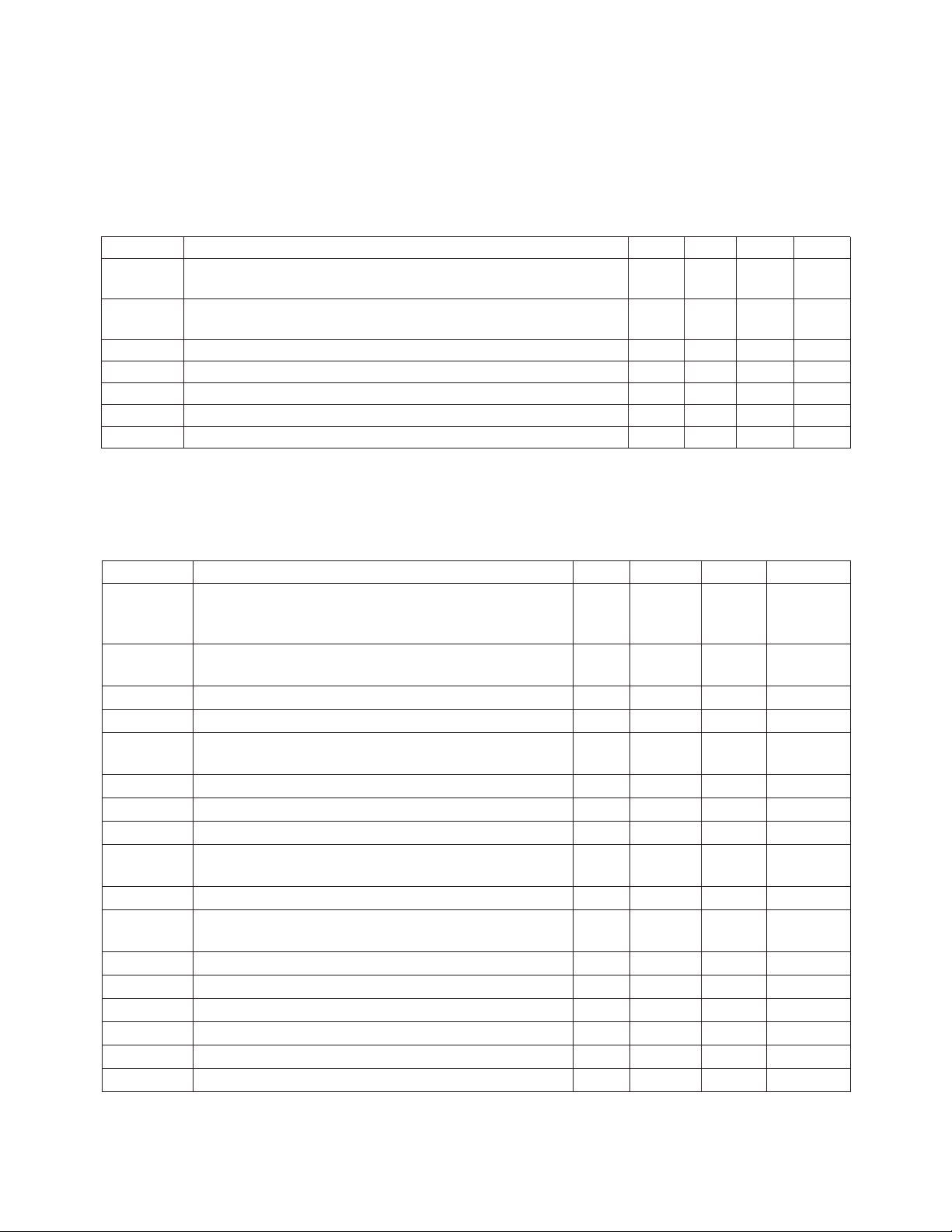
HDMP-1512 (Tx), HDMP-1514 (Rx)
DC Electrical Specifications
TC = 0°C to +85°C, VCC = 4.5 V to 5.5 V
Symbol Parameter Unit Min. Typ. Max.
V
IH,TTL
TTL Input High Voltage Level, Guaranteed high signal for V 2 5
all inputs, IIH = 100 µA
V
IL,TTL
TTL Input Low Voltage Level, Guaranteed low signal for all V 0 0.8
inputs, IIL = -1mA
V
OH,TTL
V
OL,TTL
I
CC,Tx
I
CC,Rx
PS
TH
TTL Output High Voltage Level, IOH = 1 mA V 2.4 5
TTL Output Low Voltage Level, IOL = -1 mA V 0 0.6
Transmitter VCC Supply Current, without laser biased mA 320 450
Receiver VCC Supply Current, with TTL output data 50% 1’s mA 400 550
Power Supervisor DC Threshold Voltage V 4.0 4.25 4.5
HDMP-1512 (Tx)
Laser Driver Characteristics
TC = 0°C to +85°C, VCC = 4.5 V to 5.5 V
Symbol Parameter Units Min. Typ. Max.
I
pb
I
mod
t
r,LZOUT
t
f,LZOUT
t
LZTC
V
LZCSE
V
LZBTP
V
LZMDF
A
DCOA
f
-3dB
V
LZDC_OP
V
LZDC_DCL
V
LZDC_DCH
I
LZDC_L
Z
LZDC_ACO
Z
LZMDF_ACI
I
LZMDF
Laser Diode Prebias Current Set Range (Using mA 20 130
External pnp Transistor, P1 in Figure 3, with
β > 100)
Laser Diode Modulation Current Set Range mA 25
(Peak to Peak) into 25 Ω Load
Laser Driver Rise Time, 25 Ω load, 20% to 80% psec 325
Laser Driver Fall Time, 25 Ω load, 20% to 80% psec 325
Time for V
to Discharge to Fault Threshold msec 2
LZTC
when Terminated with C = 0.1 µF
LZCSE Reference Voltage V 0.4
Bandgap Test Point Reference Voltage V 2.3
Laser Monitor Diode Feedback Voltage V 1.85
Laser Driver DC Operational Amplifier Gain, dB 35
Unloaded, see Figure 3
Laser Driver DC Operational Amplifier Bandwidth MHz 300
Recommended LZDC Operating Range, Laser Diode V VCC - 1.8 VCC - 0.75
DC Bias Control
LZDC Laser DC Bias Low Voltage Setting V VCC - 2.0
LZDC Laser DC Bias High Voltage Setting V VCC - 0.6
LZDC Load Current, over V
LZDC_OP
mA 1.3
LZDC AC Output Impedance Ω 400
LZMDF AC Input Impedance Ω 10,000
LZMDF Input Current µA615
665
Page 11
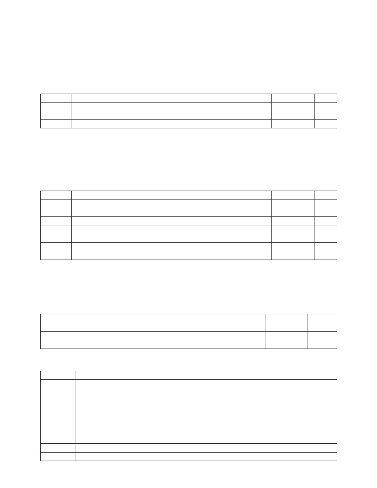
HDMP-1512 (Tx)
Timing Characteristics
TC = 0°C to +85°C, VCC = 4.5 V to 5.5 V, PPSEL = 0, SPDSEL = 1
Symbol Parameter Units Min. Typ. Max.
t
s
t
h
t_txlat Transmit Lateny
Note:
1. The Transmitter Latency is defined as the delay time from when a valid data word at TX[00:19] is clocked into the transmitter
(triggered by the rising edge of TBC during the time th) and when the first serial bit is transmitted on pins ± SO (defined by the
leading edge of the first bit transmitted).
Setup Time nsec 2
Hold Time nsec 2.3
[1]
nsec 18
HDMP-1514 (Rx)
Timing Characteristics
TC = 0°C to +85°C, VCC = 4.5 V to 5.5 V, PPSEL = 0, SPDSEL = 1
Symbol Parameter Units Min. Typ. Max.
t
flock
BLT Bit Lock Time bit times 2500
t
s
t
h
ts’ Setup Time for Data Rx[10:19] in Ping-Pong Mode nsec 6
th’ Hold Time for Data Rx[10:19] in Ping-Pong Mode nsec 8
t_rxlat Receive Latency
Note:
1. The Receiver Latency is defined as the delay time from receiving the first serial bit of a parallel data word (defined by the rising
edge of the first bit received at pins ± DI), and when that word is first clocked out at RX[00:19] (as defined by the falling edge of
RBC0 or RBC1, following time ts).
Frequency Lock Rate, Loop Filter Capacitor = 0.01 µF kHz/µsec 100
Setup Time nsec 2.5
Hold Time nsec 6.0
[1]
nsec 38
HDMP-1512 (Tx), HDMP-1514 (Rx)
Thermal Characteristics, TC = 0°C to +85°C
Symbol Parameter Units Typ.
P
P
D, Tx
D, Rx
Θ
jc
Transmitter Power Dissipation, VCC = +5 V Watt 1.6
Receiver Power Dissipation, VCC = +5 V Watt 2
Thermal Resistance, Junction to Case °C/Watt 12
I/O Type Definitions
I/O Type Definition
I-TTL Input TTL. Floats high when left open.
O-TTL Output TTL.
O-BLL 50 Ω buffer line logic output driver. Should be ac coupled to drive 50 Ω loads. It can also
drive the I-H50 inputs through differential direct coupling. Note: all unused outputs should
be terminated with 50 Ω to VCC.
I-H50 Input with internal 50 Ω terminations. Input is diode level shifted so that it can swing around
VCC. Can be driven with single-ended or differential, ac coupled configuration. To avoid
permanent damage, these inputs should not be connected to ground.
C External circuit node.
S Power supply or ground.
666
Page 12
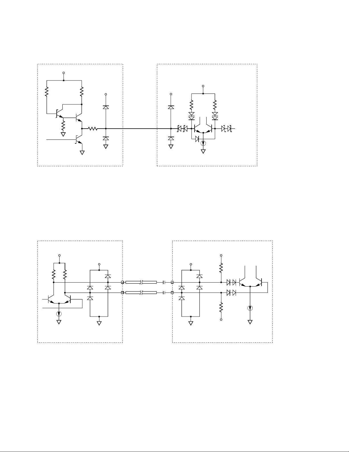
VCC_TTL
O_TTL I_TTL
VCC_TTL
VCC_LOG
72800
VCC_LOG
ESD
6 K
36
ESD
GND_LOG
GND_TTL
Figure 9. O-TTL and I-TTL Simplified Circuit Schematic.
O-BLL I-H50
VCC_HS
VCC_LOG
8080
ESD
Zo = 50 Ω
0.1 µF
ESD
ESD
GND_LOG
10 K
GND_TTL
VCC_LOG
ESD
10 K
VCC_HS
50
V
1.4 V
BB
ESD
Zo = 50 Ω
0.1 µF
ESD
ESD
GND_LOG
ESD
50
VCC_HS
GND_HS
GND_HS
ESD
ESD
GND_LOG
Figure 10. O-BLL and I-H50 Simplified Circuit Schematics. (Note: I-H50 Inputs Should Never Be Connected to Ground as
Permanent Damage to the Device May Result.)
667
Page 13
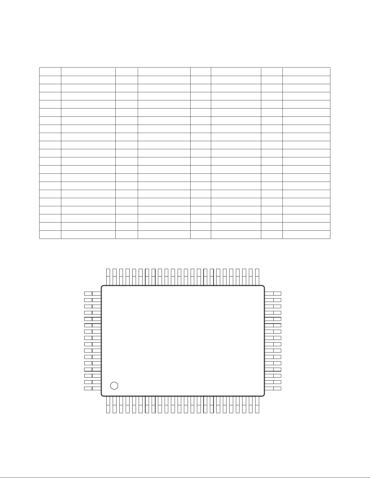
HDMP-1512 (Tx)Pin Assignments
Pin Name Pin Name Pin Name Pin Name
01 CAP1A 21 LZDC 41 VCC_TTL 61 TX[18]
02 CAP1B 22 LZMDF 42 VCC_TTL 62 TX[19]
03 GND_A 23 VCC_LZ 43 TX[00] 63 VCC_TTL
04 GND_A 24 VCC_LZ 44 TX[01] 64 VCC_TTL
05 +SO 25 GND_LZ 45 TX[02] 65 GND_TTL
06 -SO 26 GND_LZ 46 TX[03] 66 GND_TTL
07 VCC_HS1 27 LZTC 47 TX[04] 67 SPDSEL
08 +LOUT 28 LZBTP 48 TX[05] 68 VCC_LOG
09 -LOUT 29 FAULT 49 TX[06] 69 -ECLKSEL
10 GND_LZHS 30 -LZON 50 TX[07] 70 GND_LOG
11 +SI 31 GND_LOG 51 TX[08] 71 EWRAP
12 -SI 32 -COMGEN 52 TX[09] 72 VCC_LOG
13 VCC_HS2 33 VCC_LOG 53 TX[10] 73 TBC
14 LZCSE 34 PPSEL 54 TX[11] 74 GND_LOG
15 VCC_LZBG 35 GND_LOG 55 TX[12] 75 TS2
16 VCC_LZ1 36 LZPWRON 56 TX[13] 76 TS1
17 VCC_LZAC 37 VCC_LOG 57 TX[14] 77 VCC_A
18 GND_LZHS 38 NC 58 TX[15] 78 VCC_A
19 +LZOUT 39 GND_TTL 59 TX[16] 79 CAP0A
20 -LZOUT 40 GND_TTL 60 TX[17] 80 CAP0B
_TTL
_TTL
CC
CC
V
V
Tx[19]
Tx[18]
Tx[17]
Tx[16]
Tx[15]
Tx[14]
Tx[13]
Tx[12]
64 63 62 61 60 59 58 57 56 55 54 53 52 51 50 49 48 47 46 45 44 43 42 41
GND_TTL
GND_TTL
SPDSEL
VCC_LOG
-ECLKSEL
GND_LOG
EWRAP
V
_LOG
CC
TBC
GND_LOG
TS2
TS1
_A
V
CC
V
_A
CC
CAP0A
CAP0B
65
66
67
68
69
70
71
72
73
74
75
76
77
78
79
80
1 2 3 4 5 6 7 8 9 10 11 12 13 14 15 16 17 18 19 20 21 22 23 24
CAP1A
CAP1B
GND_A
GND_A
HDMP-1512
TOP VIEW
-SO
+SO
_HS1
- LOUT
+ LOUT
CC
V
GND_LZHS
Figure 11. HDMP-1512 (Tx) Package Layout, Top View.
Tx[11]
Tx[10]
-SI
+SI
Tx[09]
Tx[08]
_HS2
LZCSE
CC
V
Tx[07]
Tx[06]
_LZ1
_LZBG
CC
V
CC
V
Tx[05]
Tx[04]
_LZAC
CC
V
GND_LZHS
Tx[03]
Tx[02]
-LZOUT
+LZOUT
Tx[01]
Tx[00]
LZDC
LZMDF
_TTL
CC
V
_LZ
CC
V
_TTL
CC
V
40
39
38
37
36
35
34
33
32
31
30
29
28
27
26
25
_LZ
CC
V
GND_TTL
GND_TTL
NC
_LOG
V
CC
LZPWRON
GND_LOG
PPSEL
V
_LOG
CC
-COMGEN
GND_LOG
-LZON
FAULT
LZBTP
LZTC
GND_LZ
GND_LZ
668
Page 14
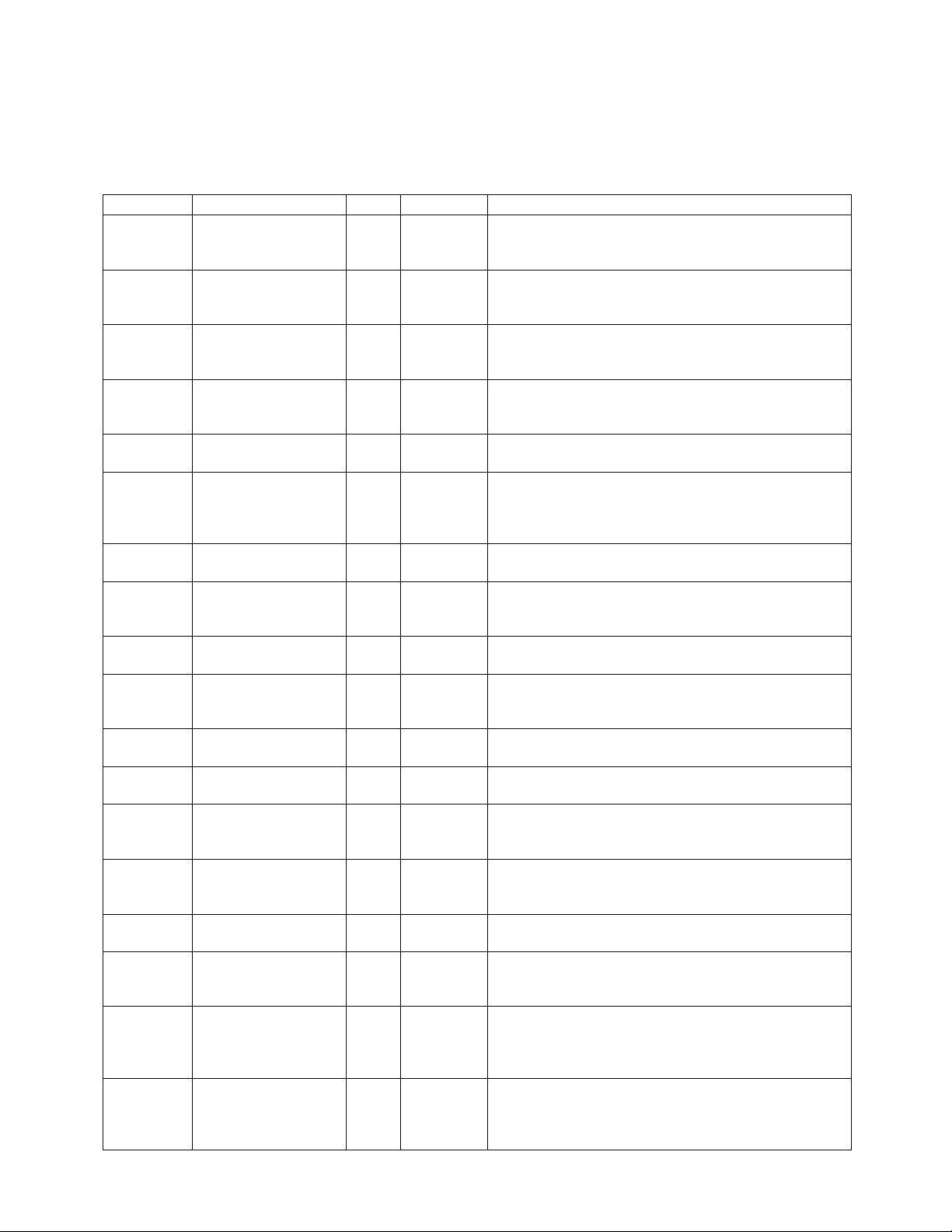
HDMP-1512 (Tx), Signal Definitions
Symbol Signal Name I/O Logic Type Description
CAP0[A:B] Loop Filter Capacitor C PLL filter capacitor should be connected from pins
Pins [79,80] 79 and 80 to pins 1 and 2 (typical value = 0.01 µF).
See Figures 18, 19, 20, and 21.
CAP1[A:B] Loop Filter Capacitor C PLL filter capacitor should be connected from pins
Pins [1,2] 79 and 80 to pins 1 and 2 (typical value = 0.01 µF).
See Figures 18, 19, 20, and 21.
-COMGEN Comma Generate Input TTL An active low input, causes the transmitter to
Pin [32] internally generate the positive disparity K28.5 byte
(0011111010) for transmission.
-ECLKSEL External Clock Select Input TTL An active low input, selects the TBC inputs to be used
Pin [69] as the serial clock, bypassing the PLL. Used mainly
for testing.
EWRAP Enable Wrap Input TTL Works in conjunction with TS1 and TS2 to specify
Pin [71] input and output ports.
FAULT Laser Fault Indicator Output TTL Indicates the laser output level has moved outside of
Pin [29] the window detector set boundary and the laser test
capacitor (LZTC) has discharged to a fault level. This
output is reset by the -LZON pin.
GND_A Analog Ground S Normally 0 volts. Used to provide a clean ground plane
Pins [3,4] for the critical PLL and high speed analog cells.
GND_LOG Logic Ground S Normally 0 volts. Used for all internal PECL logic.
Pins [31,35,70,74] Should be completely isolated from the noisy TTL
ground.
GND_LZ Laser Ground S Normally 0 volts. Used for all laser circuitry.
Pins [25,26]
GND_LZHS Laser High Speed S Normally 0 volts.
Ground
Pins [10,18]
GND_TTL TTL Ground S Normally 0 volts. Used for all TTL I/O buffer cells.
Pins [39,40,65,66]
± LOUT Local Serial Data Output BLL High speed data port, typically connected to the ± LIN
Pins [8,9] port on the local receiver during serial wrap mode.
LZBTP Laser Bandgap Test C This pin is internally set to 2.3 VDC and normally
Point should connect to one terminal of the laser DC bias
Pin [28] resistor (pot1 Figure 3).
LZCSE Laser Current Source C Used to set the bias current of the AC laser driver.
Emitter Typical use is shown in Figure 3 where pot2 is used to
Pin [14] set the laser modulation depth.
LZDC Laser DC Drive C Used to control the laser diode DC bias (Figure 3).
Pin [21]
± LZOUT Laser Driver Serial C AC driver to the laser diode. The outputs should be AC
Output coupled to the laser bias circuit.
Pins [19,20]
LZMDF Laser Monitor Diode C Connects to the laser monitor diode and one terminal of
Feedback the laser DC bias resistor (pot1). Under normal
Pin [22] operating conditions, the voltage on this pin will
be 1.85 V.
-LZON Laser Control and Input TTL The laser diode is turned on (active low) or off (high)
Reset with this input. In the off state the capacitor on pin
Pin [30] LZTC charges, resetting the window
detector (Figure 3).
669
Page 15
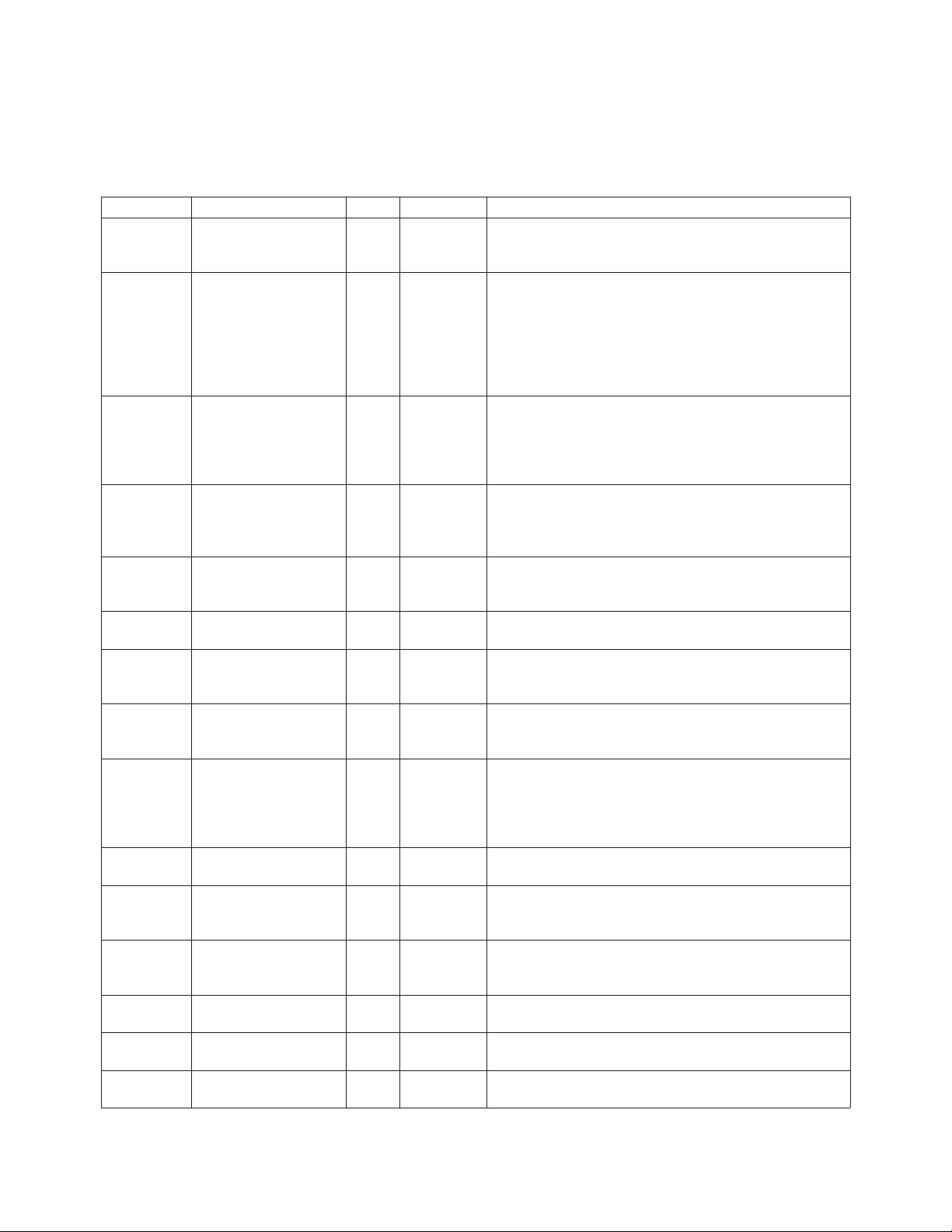
HDMP-1512 (Tx), Signal Definitions (cont’d.)
Symbol Signal Name I/O Logic Type Description
LZPWRON Laser Power On Input TTL Used in conjunction with the dual loss of light
Pin [36] detectors and the OFC circuit to assure the system is
ready to power up the laser.
LZTC Laser Timing Cap C The capacitor connected to this pin will be pre-
Pin [27] charged at power-up. During operation, if the window
detector detects the laser bias to be out of range, this
capacitor will begin to discharge. If the condition lasts
long enough, the capacitor voltage will fall below the
fault level and the FAULT pin will go high. Nominal
fault level is <1.0 volts.
PPSEL Ping-Pong Select Input TTL A high signal applied to this pin causes the transmitter
Pin [34] to clock the data in by alternating between data byte 0
on the rising edge of TBC and data byte 1 one half
clock cycle later. When this pin is low, both data bytes
are clocked in on the rising edge of TBC.
± SI Laser External Serial Input H50 The signal on this pin is input directly to the internal
Input laser driver circuitry or the LOUT pin. This input is
Pins [11,12] selected with the proper setting of TS1, TS2 and
EWRAP (see Input/Output Select table).
± SO Cable Serial Data Output BLL High speed data output port. See Input/Output Select
Output table to enable this output.
Pins [5,6]
SPDSEL Serial Speed Select Input TTL Sets the chip to operate at the serial data rate of 1062.5
Pin [67] Mbaud (high) or 531.25 Mbaud (low).
TBC Transmit Byte Clock Input TTL A 53.125 Mhz clock supplied by the host system. This
Pin [73] reference clock is multiplied by 10 or 20 to generate
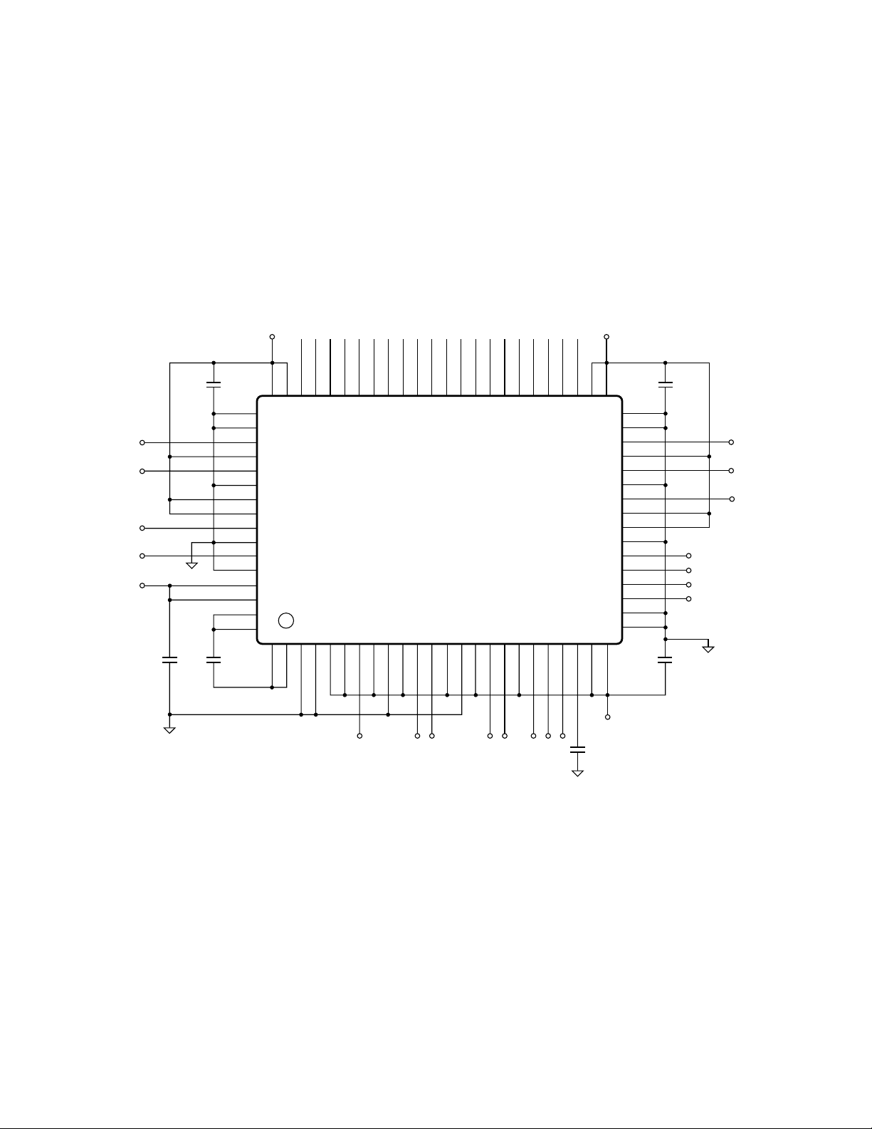
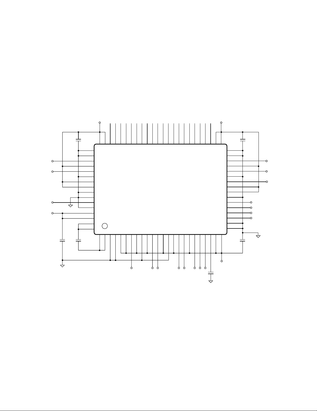
the serial bit clock (531.25 MHz or 1062.5 MHz).
TS[1:2] Input/Output Select Input TTL TS1 and TS2 work in conjunction with EWRAP to
Input specify active input and output ports.
Pins [75,76]
TX[00.19] Data Inputs Input TTL Two, 10 bit, pre-encoded data bytes. Byte 0 is
Pins [43:62] comprised of bits TX[00:09] and byte 1 is comprised of
bits TX[10:19]. The serialized bit stream is
transmitted TX[00] through TX[09] then TX[10]
through TX[19].
VCC_A Analog Supply S Provides a clean power source for the critical PLL
Pins [77, 78] and high speed analog cells. Normally +5.0 volts.
VCC_HS1 High Speed Supply 1 S Provides a clean power source for the high speed
Pin [7] cells. Noise on this line should be minimized for best
performance. Normally +5.0 volts.
VCC_HS2 High Speed Supply 2 S Provides a clean power source for the high speed
Pin [13] cells. Noise on this line should be minimized for best
performance. Normally +5.0 volts.
VCC_LOG Logic Power Supply S Used for all internal PECL logic. Isolate from the
Pins [33,37,68,72] noisy TTL supply. Normally +5.0 volts.
VCC_LZ Laser Power Supply S Power supply for low speed laser driver circuitry.
Pins [23,24] Normally +5.0 volts.
VCC_LZ1 Laser Power Supply S Power supply for all laser driver AC circuitry.
Pin [16] Normally +5.0 volts.
670
Page 16
HDMP-1512 (Tx), Signal Definitions (cont’d.)
Symbol Signal Name I/O Logic Type Description
VCC_LZAC Laser Power Supply S Power supply for all high speed laser driver circuitry.
Pin [17] Normally +5.0 volts.
VCC_LZBG Laser Power Supply S Power supply for low speed laser driver circuitry.
Pins [15] Normally +5.0 volts.
VCC_TTL TTL Power Supply S Power supply for all TTL buffer I/O cells. Normally
Pins [41,42,63,64] +5.0 volts.
NC Pin [38] No connection.
_TTL
GND_TTL
GND_TTL
RBC[1]
_LOG
V
CC
RBC[0]
GND_LOG
SPDSEL
V
_LOG
CC
L_UNUSE
GND_LOG
COM_DET
PPSEL
V
_A
CC
V
_A
CC
CAP0A
CAP0B
_TTL
CC
CC
V
V
Rx[00]
Rx[01]
Rx[02]
Rx[03]
Rx[04]
Rx[05]
Rx[06]
Rx[07]
Rx[08]
Rx[09]
Rx[10]
Rx[11]
Rx[12]
Rx[13]
Rx[14]
Rx[15]
Rx[16]
Rx[17]
64 63 62 61 60 59 58 57 56 55 54 53 52 51 50 49 48 47 46 45 44 43 42 41
65
66
67
68
69
70
71
72
73
74
75
76
77
78
79
80
1 2 3 4 5 6 7 8 9 10 11 12 13 14 15 16 17 18 19 20 21 22 23 24
HDMP-1514
TOP VIEW
Rx[18]
Rx[19]
_TTL
CC
V
_TTL
CC
V
40
39
38
37
36
35
34
33
32
31
30
29
28
27
26
25
GND_TTL
GND_TTL
EN_CDET
_LOG
V
CC
-LCK_REF
GND_LOG
EWRAP
V
_LOG
CC
-EQEN
GND_LOG
NC
LOLB
LOLA
POR
GND_HS
GND_HS
CAP1A
CAP1B
GND_A
GND_A
-TCLKSEL
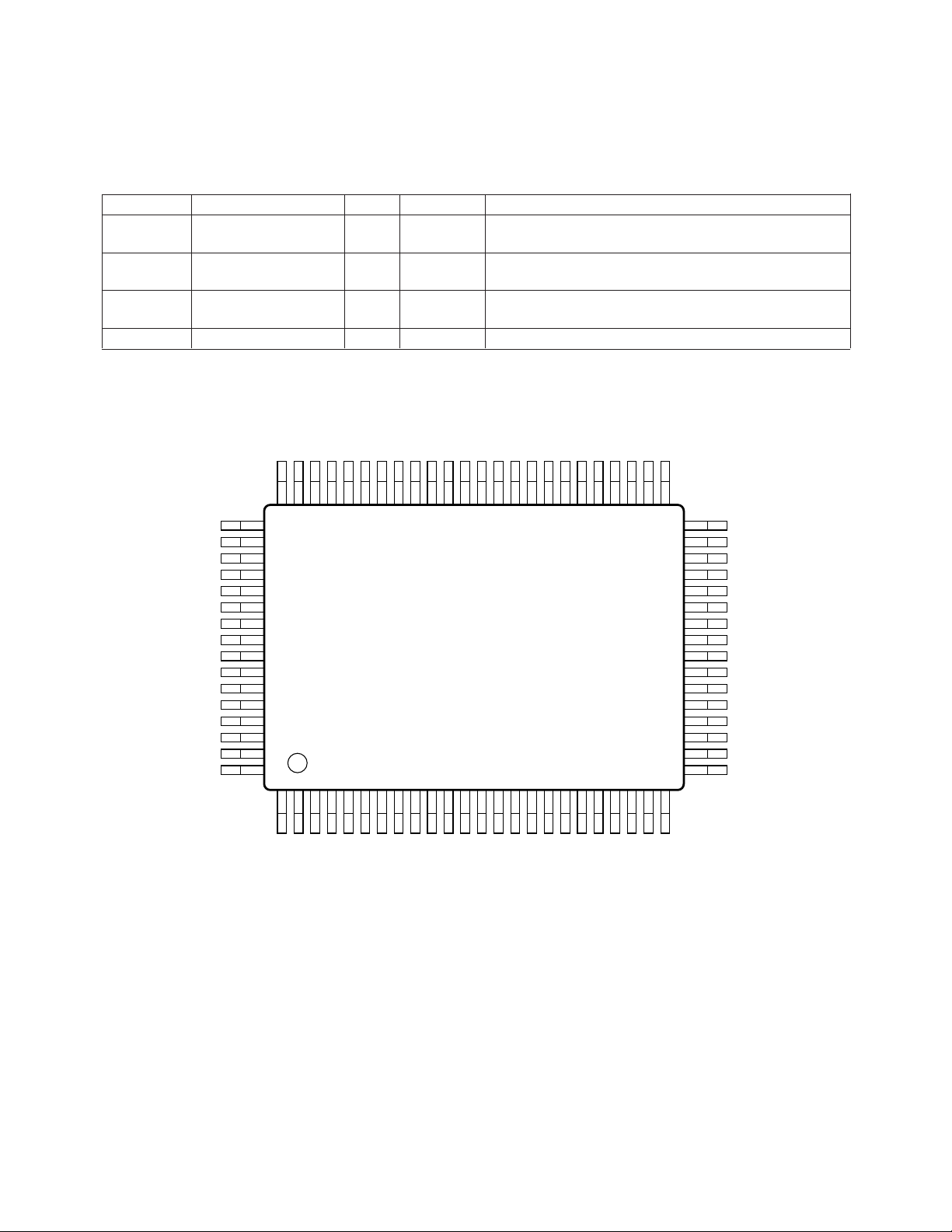
Figure 12. HDMP-1514 (Rx) Package Layout.
P_RXTEMP
N_RXTEMP
CLKIN (& TCLK)
NC
_TTLA
CC
V
GND_TTLA
NC
_HS
CC
V
_HS2
CC
GND_HS
V
-LIN
+LIN
_HS2
CC
V
-DI
+DI
PS_CT
DR_REF
_HS
CC
V
_HS
CC
V
671
Page 17
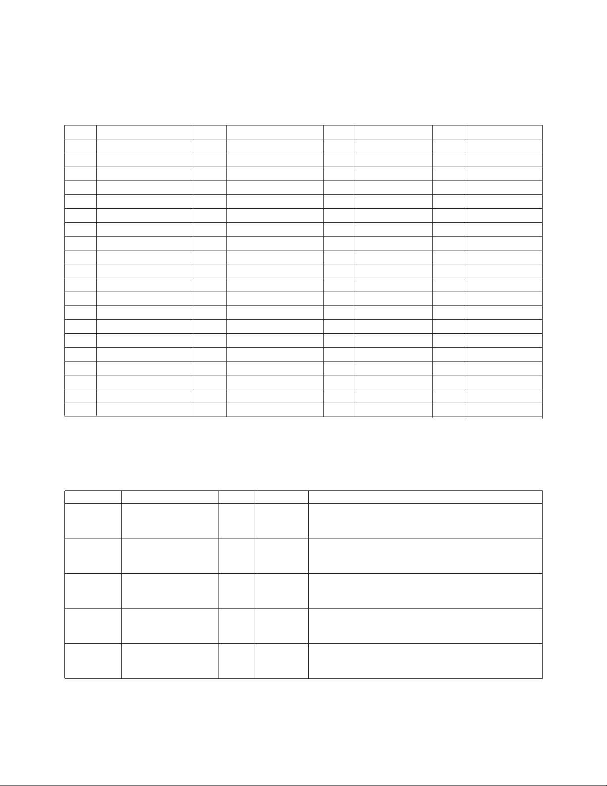
HDMP-1514 (Rx) Pin Assignments
Pin Name Pin Name Pin Name Pin Name
01 CAP1A 21 DR_REF 41 VCC_TTL 61 RX[01]
02 CAP1B 22 PS_CT 42 VCC_TTL 62 RX[00]
03 GND_A 23 VCC_HS 43 RX[19] 63 VCC_TTL
04 GND_A 24 VCC_HS 44 RX[18] 64 VCC_TTL
05 -TCLKSEL 25 GND_HS 45 RX[17] 65 GND_TTL
06 N_RXTEMP 26 GND_HS 46 RX[16] 66 GND_TTL
07 CLKIN (TCLK) 27 -POR 47 RX[15] 67 RBC[1]
08 P_RXTEMP 28 LOLA 48 RX[14] 68 VCC_LOG
09 GND_TTLA 29 LOLB 49 RX[13] 69 RBC[0]
10 VCC_TTLA 30 NC 50 RX[12] 70 GND_LOG
11 NC 31 GND_LOG 51 RX[11] 71 SPDSEL
12 NC 32 -EQEN 52 RX[10] 72 VCC_LOG
13 VCC_HS 33 VCC_LOG 53 RX[09] 73 L_UNUSE
14 GND_HS 34 EWRAP 54 RX[08] 74 GND_LOG
15 VCC_HS2 35 GND_LOG 55 RX[07] 75 COM_DET
16 -LIN 36 -LCK_REF 56 RX[06] 76 PPSEL
17 +LIN 37 VCC_LOG 57 RX[05] 77 VCC_A
18 VCC_HS2 38 EN_CDET 58 RX[04] 78 VCC_A
19 -DI 39 GND_TTL 59 RX[03] 79 CAP0A
20 +DI 40 GND_TTL 60 RX[02] 80 CAP0B
HDMP-1514 (Rx), Signal Definitions
Symbol Signal Name I/O Logic Type Description
CAP0[A:B] Loop Filter Capacitor C PLL filter capacitor should be connected from pins
Pins [79,80] 79 and 80 to pins 1 and 2 (typical value = 0.01 µF).
See Figures 18, 19, 20, and 21.
CAP1[A:B] Loop Filter Capacitor C PLL filter capacitor should be connected from pins
Pins [1,2] 79 and 80 to pins 1 and 2 (typical value = 0.01 µF).
See Figures 18, 19, 20, and 21.
CLKIN Receive Reference Input TTL A 53.125 MHz clock supplied by the host system.
(TCLK) Clock CLKIN is used by the internal PLL to acquire frequency
Pin [7] lock when the -LCKREF input is brought low.
COM_DET Comma Detect Output TTL Indicates the detection of a comma character
Pin [75] (K28.5 of positive disparity). It is only active when
EN_CDET is high.
± DI Serial Data Inputs Input H50 High speed serial data inputs, selected when EWRAP
Pins [19,20] is set low. An optional cable equalizer may also be
enabled, see EQEN.
672
Page 18
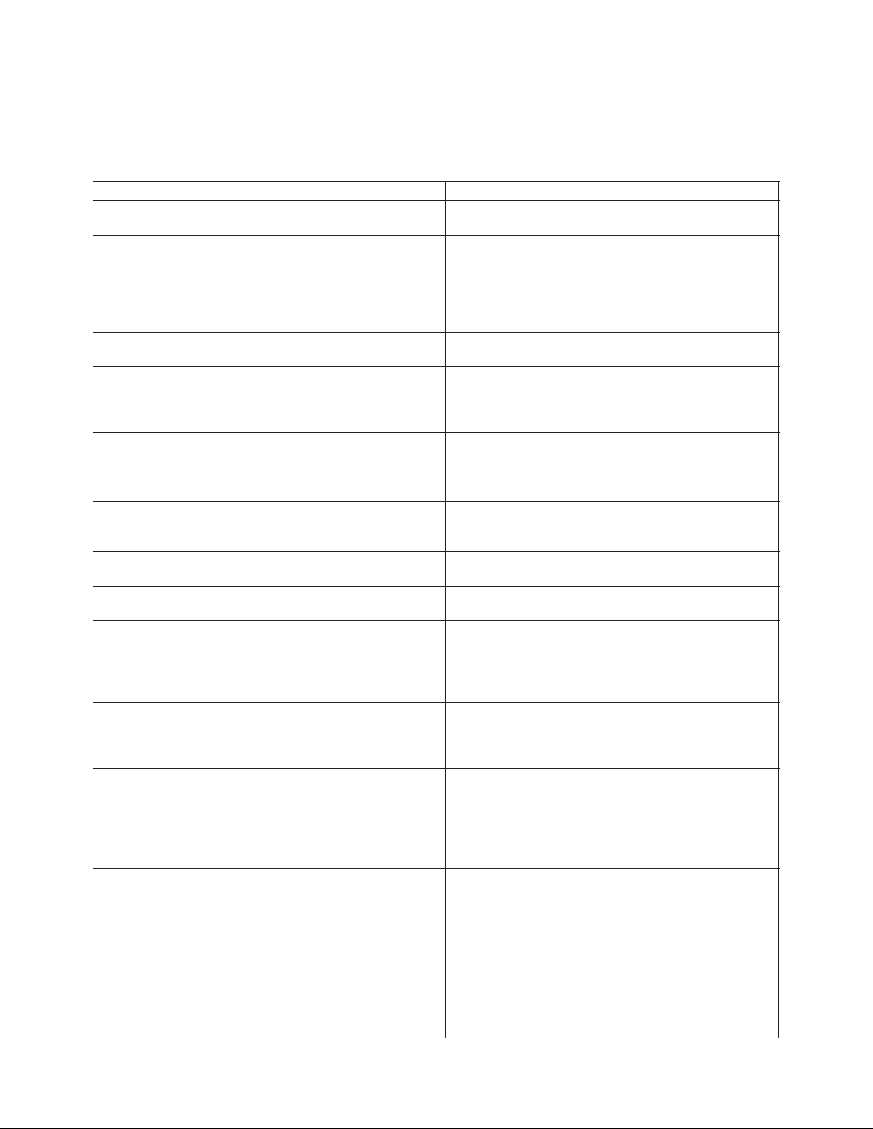
HDMP-1514 (Rx), Signal Definitions (cont’d.)
Symbol Signal Name I/O Logic Type Description
DR_REF Receiver Reference C This node is used to set the peak-to-peak signal level
Pin [21] of the loss of light detection circuitry.
EN_CDET Enable Comma Detect Input TTL When high, the receiver will reset internal clocks and
Pin [38] registers when an incoming comma character (K28.5)
of positive disparity (0011111xxx) is detected. When
low, clocks and registers will not reset and the comma
detect output is disabled. Comma detect is also disabled
whenever -LCK_REF is set low.
-EQEN Equalizer Enable Input Input TTL When set low, the internal cable equalizer amplifier on
Pin [32] the ± DI lines is enabled.
EWRAP Enable Wrap Input TTL When set high, the high speed data is taken from the
Pin [71] ± LIN port, enabling the data input from the local
transmitter. When this input is set low, the high speed
input is taken from the ± DI lines.
GND_A Analog Ground S Normally 0 volts. Used to provide a clean ground plane
Pins [3,4] for the critical PLL and high speed analog cells.
GND_HS High Speed Ground S Normally 0 volts.
Pins [14,25,26]
GND_LOG Logic Ground S Normally 0 volts. Used for all internal PECL logic.
Pins[31,35,70,74] Should be completely isolated from the noisy TTL
ground.
GND_TTL TTL Ground S Normally 0 volts. Used for all TTL I/O buffer cells.
Pins [39,40,65,66]
GND_TTLA TTL Ground S Normally 0 volts.
Pin [9]
-LCK_REF Lock to Reference Input TTL A low input causes the internal PLL to acquire
Pin [36] frequency lock on the external reference signal applied
at CLKIN. To assure lock, this pin should be held low
for at least 500 µsec and held high at all other times. A
low input disables the comma detect function.
L_UNUSE Link Unusable Input TTL Typically supplied from open fiber control circuitry.
Pin [73] Used in conjunction with EWRAP and -LCK_REF to
keep the internal Vco near operational frequency,
optimizing frequency lock times.
± LIN Local Serial Data Input H50 High speed data port, typically connected to the ± LOUT
Pins [16,17] port on the local transmitter when in serial wrap mode.
LOLA Loss of Light Output TTL A high signal on this pin indicates the amplitude of
Signal the input serial data has fallen below a preset level
Pin [28] (see DR_REF) or no transitions have been detected
within 4 cycles of TBC.
LOLB Loss of Light Output TTL A high signal on this pin indicates the amplitude of
Signal the input serial data has fallen below a preset level
Pin [29] (see DR_REF) or no transitions have been detected
within 4 cycles of TBC.
N_RXTEMP Temperature Monitor C Used in conjunction with pin 8 (P_RXTEMP) to
Pin [6] monitor the on-chip temperature diode (Cathode.)
P_RXTEMP Temperature Monitor C Used in conjunction with pin 6 (N_RXTEMP) to
Pin [8] monitor the on-chip temperature diode (Anode.)
-POR Power on Reset Output TTL Active low output. Monitors the power supply voltage
Pin [27] on startup to assure V
is at the proper DC level.
CC
673
Page 19
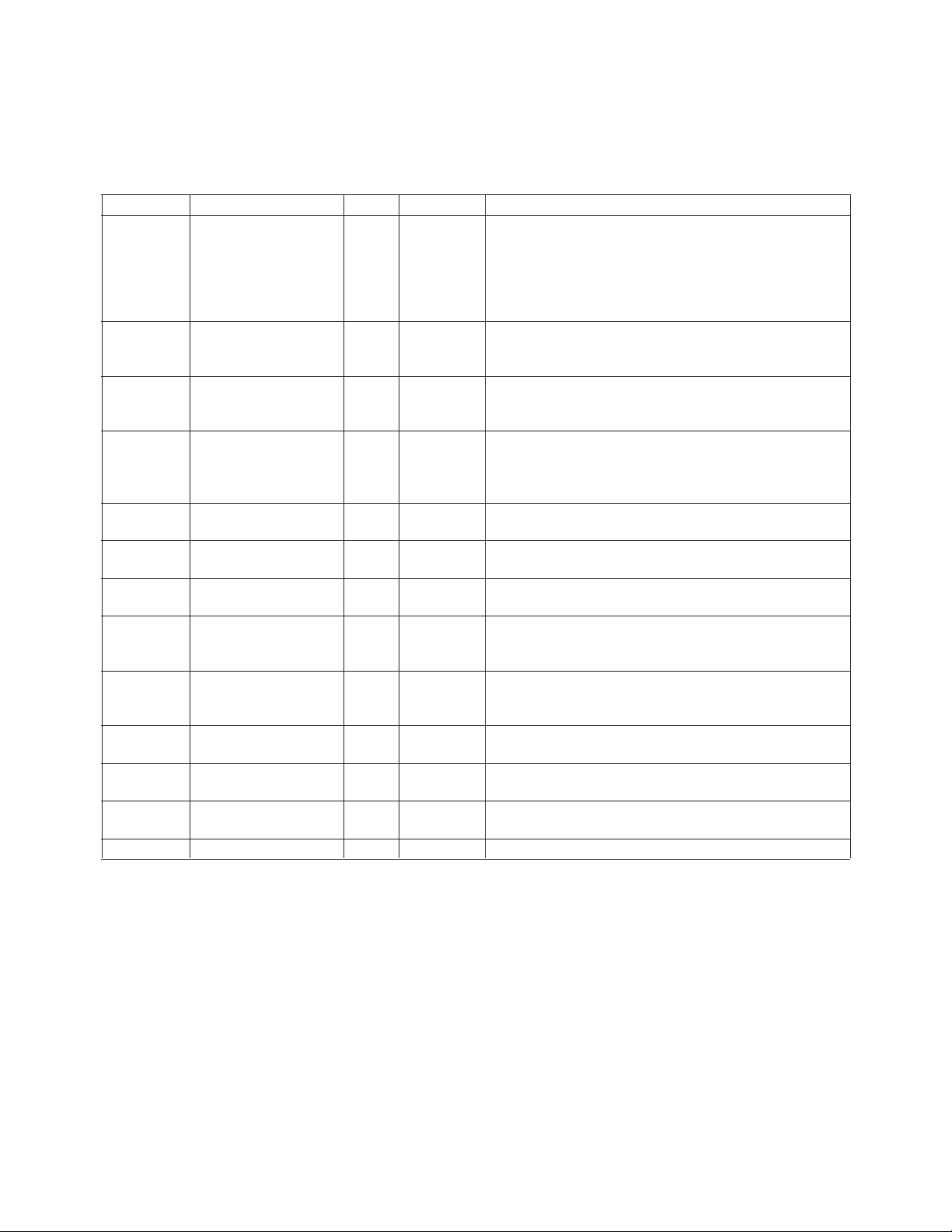
HDMP-1514 (Rx), Signal Definitions (cont’d.)
Symbol Signal Name I/O Logic Type Description
PPSEL Ping-Pong Select Input TTL A high input instructs the receiver to clock the data
Pin [76] out in ping-pong mode. Byte 0 will be clocked out on
the falling edge of RBC0 and byte 1 will be clocked out
on the falling edge of RBC1. A low input instructs the
receiver to clock both data bytes out on the falling edge
of RBC0.
PS_CT Power Supply Timing C Pin for connecting the timing capacitor for the power
Cap supervisor circuit.
Pin [22]
RBC[0:1] Receive Byte Clocks Output TTL Two clocks, 180° out of phase, generated from the
Pin [67, 69] recovered data. Used to clock out the two 10 bit data
bytes.
RX[00:19] Data Outputs Output TTL Two, 10 bit, bytes. Byte 0 is comprised of bits
Pins [43, 62] RX[00:09] and byte 1 is comprised of bits RX[10:19].
The serialized bit stream is received TX[00] through
TX[09] then TX[10] through TX[19].
SPDSEL Serial Speed Select Input TTL Sets the chip to operate at the serial data rate of 1062.5
Pin [71] Mbaud (high) or 531.25 Mbaud (low).
-TCLKSEL Test Clock Select Input TTL An applied low selects CLKIN as the serial/bit-rate clock
Pin [5] and bypasses the internal PLL. Used for testing only.
VCC_A Analog Supply S Provides a clean power source for the critical PLL
Pins [77, 78] and high speed analog cells. Normally +5.0 volts.
VCC_HS1 High Speed Supply S Provides a clean power source for the high speed
Pins [13,23,24] receiver cell I-H50. Noise on this line should be
minimized for best performance. Normally +5.0 volts.
VCC_HS2 High Speed Supply 2 S Provides a clean power source for the high speed
Pins [15,18] receiver cell I-H50. Noise on this line should be
minimized for best performance. Normally +5.0 volts.
VCC_LOG Logic Power Supply S Used for all internal PECL logic. Isolate from the
Pins [33,37,68,72] noisy TTL supply. Normally +5.0 volts.
VCC_TTL TTL Power Supply S Power supply for all TTL buffer I/O cells. Normally
Pins [41,42,63,64] +5.0 volts.
VCC_TTLA TTL Power Supply S Power supply for all TTL I/O buffer cells. Normally
Pin [10] +5.0 volts.
NC Pins [11,12,30] No connection.
674
Page 20
Package Description and Assembly Recommendations
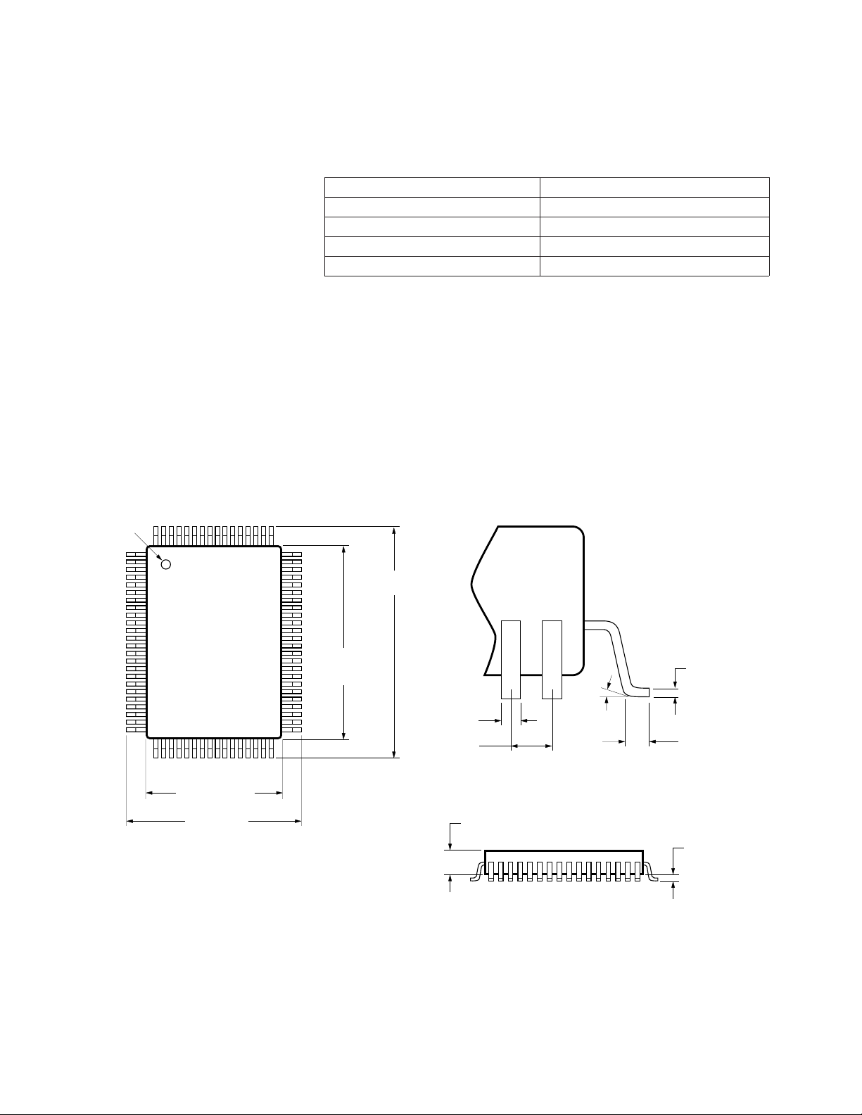
The HDMP-1512 and HDMP1514 are available in the industry
standard M-Quad 80 lead
package. The outline dimensions
conform to JEDEC plastic QFP
specifications and are shown in
Figure 13. The package material
is aluminum. To facilitate surface
mounting, the leads have been
formed into a “GullWing” configuration. We recommend keeping
the package temperature, TC,
below 85°C. Forced air cooling
may be required.
PIN #1 ID
M-Quad 80 Package Specifications
Item Specification
Package Material Aluminum
Lead Finish Material 85/15 Sn/Pb
Lead Finish Thickness 300-600 µinches
Lead Coplanarity 0.004 inches maximum
23.20 ± 0.10
(0.913 ± 0.004)
TOP VIEW
+ 0.18
19.786
- 0.08
+ 0.008
(
0.779
+ 0.16
13.792
- 0.04
+ 0.008
(
0.543
17.20 ± 0.10
(0.677 ± 0.004)
ALL DIMENSIONS ARE IN MILLIMETERS (INCHES).
Figure 13. HDMP-1512 and HDMP-1514 Package Outline.
- 0.002
)
- 0.002
)
0.35
(0.014 )
0.80
(0.0315 )
TYP.
TYP.
2.64 ± 0.13
(0.104 ± 0.005)
7 °
0.15
(0.006)
0.80 ± 0.13
(0.031 ± 0.005)
0.38 ± 0.05
(0.015 ± 0.002)
675
Page 21
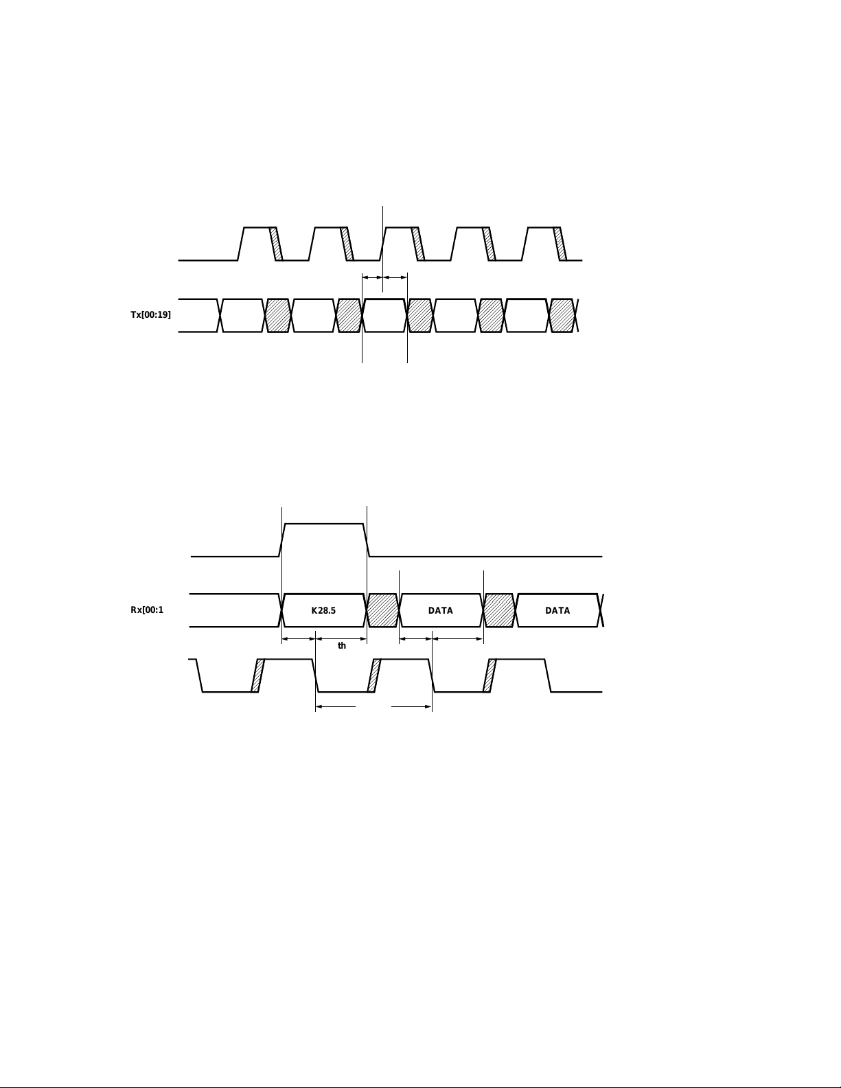
TBC
ts
th
Tx[00:19]
DATADATA DATA DATA DATA
Figure 14. HDMP-1512 (Transmitter) Timing Diagram, with PPSEL = 0.
COM_DET
Rx[00:19]
RBCO
K28.5 DATA DATA
ts
th
18.8 ns
ts th
Figure 15. HDMP-1514 (Receiver) Timing Diagram, with PPSEL = 0.
676
Page 22
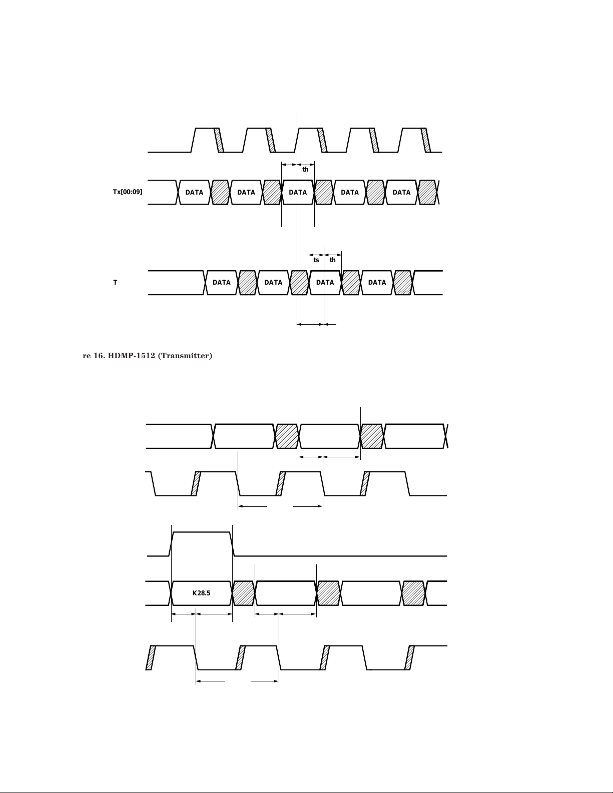
TBC
ts
th
Tx[00:09]
Tx[10:19]
DATADATA DATA DATA DATA
ts
th
DATADATA DATA DATA
1/2 CLOCK CYCLE (TBC)
Figure 16. HDMP-1512 (Transmitter) Timing Diagram In Ping-Pong Mode, PPSEL = 1.
Rx[10:19]
DATA DATA DATA
ts th
RBC1
18.8 ns
COM_DET
Rx[00:09]
RBC0
K28.5
ts'
th'
18.8 ns
DATA DATA
ts' th'
Figure 17. HDMP-1514 (Receiver) Timing Diagram in Ping-Pong Mode, with PPSEL = 1.
677
Page 23
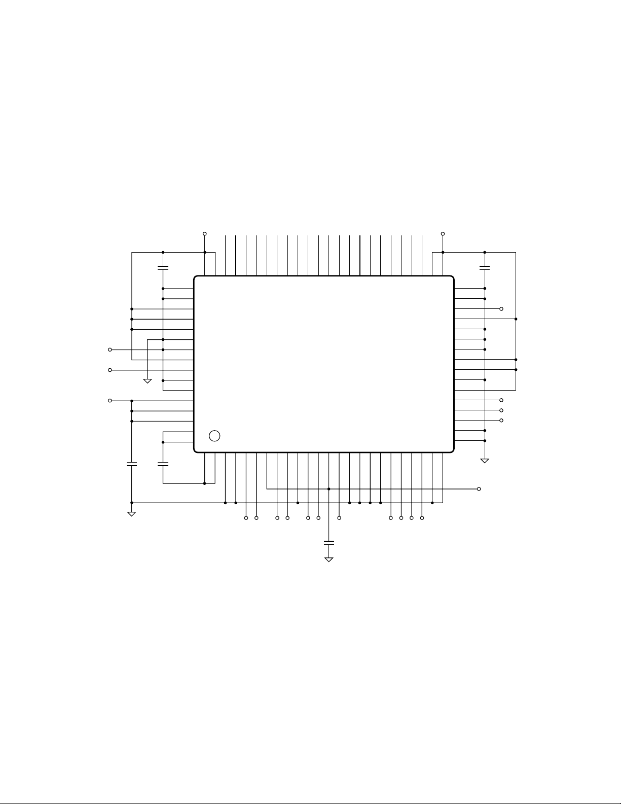
+5.0 V
Tx[19]
Tx[18]
Tx[17]
Tx[16]
Tx[15]
Tx[14]
Tx[13]
Tx[12]
Tx[11]
Tx[10]
Tx[09]
Tx[08]
Tx[07]
Tx[06]
Tx[05]
Tx[04]
Tx[03]
Tx[02]
Tx[01]
Tx[00]
+5.0 V
EWRAP
TBC
+5.0 V
0.1 µF
0.1 µF
0.01 µF
64 63 62 61 60 59 58 57 56 55 54 53 52 51 50 49 48 47 46 45 44 43 42 41
65
66
67
68
69
70
71
72
73
74
75
76
77
78
79
80
1 2 3 4 5 6 7 8 9 10 11 12 13 14 15 16 17 18 19 20 21 22 23 24
HDMP-1512
TOP VIEW
-Si
+So
-So
- LOUT
+ LOUT
+Si
NC
0.1 µF
NCNCNC
NC
0.1 µF
40
39
38
37
36
35
34
33
32
31
30
29
28
27
26
25
NC
NC
NC
NC
+5.0 V
Figure 18. Typical Transmitter Pin Terminations for Applications Requiring High Speed Serial Copper Drivers (±So).
Laser Driver Outputs are Disabled. For 1062.5 MBd Operation Only, SPDSEL (pin 67) Set High, Non Ping-Pong Mode
(PPSEL = 0).
678
Page 24
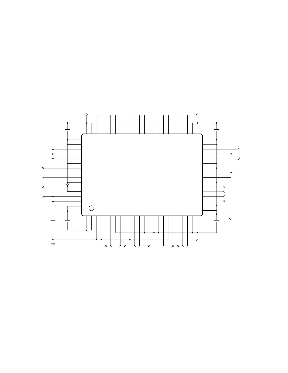
+5.0 V
Tx[19]
Tx[18]
Tx[17]
Tx[16]
Tx[15]
Tx[14]
Tx[13]
Tx[12]
Tx[11]
Tx[10]
Tx[09]
Tx[08]
Tx[07]
Tx[06]
Tx[05]
Tx[04]
Tx[03]
Tx[02]
Tx[01]
Tx[00]
+5.0 V
EWRAP
TBC
TS1,2
+5.0 V
0.1 µF
0.1 µF
0.01 µF
64 63 62 61 60 59 58 57 56 55 54 53 52 51 50 49 48 47 46 45 44 43 42 41
65
66
67
68
69
70
71
72
73
74
75
76
77
78
79
80
1 2 3 4 5 6 7 8 9 10 11 12 13 14 15 16 17 18 19 20 21 22 23 24
HDMP-1512
TOP VIEW
-Si
+So
-So
+ LOUT
+Si
- LOUT
LZCSE*
_LZAC*
CC
V
-LZOUT*
+LZOUT*
LZDC*
LZMDF*
40
39
38
37
36
35
34
33
32
31
30
29
28
27
26
25
+5.0 V
0.1 µF
NC
LZPWRON*
-LZON*
FAULT*
LZBTP*
LZTC*
0.1 µF
Figure 19. Typical Transmitter Pin Terminations for Applications Using the On-Chip Laser Driver. For Details of the
Laser Driver Connections, Indicated by “*,” see Figure 3 on page 4. For 1062.5 MBd Operation Only, SPDSEL (pin 67) Set
High, Non Ping-Pong Mode (PPSEL = 0).
679
Page 25
+5.0 V
Rx[00]
Rx[01]
Rx[02]
Rx[03]
Rx[04]
Rx[05]
Rx[06]
Rx[07]
Rx[08]
Rx[09]
Rx[10]
Rx[11]
Rx[12]
Rx[13]
Rx[14]
Rx[15]
Rx[16]
Rx[17]
Rx[18]
Rx[19]
+5.0 V
RBC1
RBC0
LUNUSE
COM_DET
+5.0 V
0.1 µF
0.1 µF
0.01 µF
64 63 62 61 60 59 58 57 56 55 54 53 52 51 50 49 48 47 46 45 44 43 42 41
65
66
67
68
69
70
71
72
73
74
75
76
77
78
79
80
1 2 3 4 5 6 7 8 9 10 11 12 13 14 15 16 17 18 19 20 21 22 23 24
HDMP-1514
TOP VIEW
NC
NC
REFCLK
-LIN
+LIN
-DIN
+DIN
NC
0.47 µF
40
39
38
37
36
35
34
33
32
31
30
29
28
27
26
25
+5.0 V
0.1 µF
EN_CDET
-LCK_REF
EWRAP
NC
LOLB
LOLA
-POR
0.1 µF
Figure 20. Typical Receiver Pin Terminations for Applications Using High Speed Serial Copper Links (±DIN). For 1062.5
MBd Operation Only, SPDSEL (pin 71) Set High, Non Ping-Pong Mode (PPSEL = 0).
680
Page 26
+5.0 V
Rx[00]
Rx[01]
Rx[02]
Rx[03]
Rx[04]
Rx[05]
Rx[06]
Rx[07]
Rx[08]
Rx[09]
Rx[10]
Rx[11]
Rx[12]
Rx[13]
Rx[14]
Rx[15]
Rx[16]
Rx[17]
Rx[18]
Rx[19]
+5.0 V
RBC1
RBC0
COM_DET
+5.0 V
0.1 µF
0.1 µF
0.01 µF
64 63 62 61 60 59 58 57 56 55 54 53 52 51 50 49 48 47 46 45 44 43 42 41
65
66
67
68
69
70
71
72
73
74
75
76
77
78
79
80
1 2 3 4 5 6 7 8 9 10 11 12 13 14 15 16 17 18 19 20 21 22 23 24
HDMP-1514
TOP VIEW
NC
NC
REFCLK
-LIN
+LIN
-DIN
+DIN
NC
40
39
38
37
36
35
34
33
32
31
30
29
28
27
26
25
+5.0 V
0.47 µF
0.1 µF
EN_CDET
-LCK_REF
EWRAP
NC
LOLB
LOLA
-POR
0.1 µF
Figure 21. Typical Receiver Pin Terminations for Applications Using High Speed Fiber Links (±DIN). For 1062.5 MBd
Operation Only, SPDSEL (pin 71) Set High, Non Ping-Pong Mode (PPSEL = 0).
681
 Loading...