

Page 1
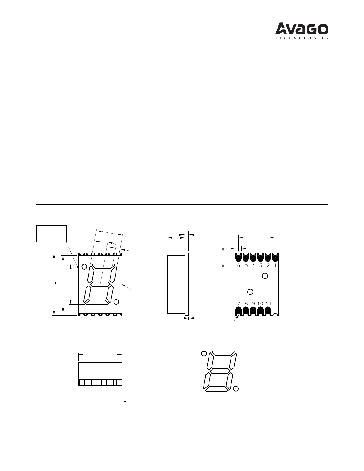
2. Tolerance are 0.25mm unless otherwise noted.
1. All dimensions are in millimeters.
Notes:
PART NO.
4.6
10.0
o
0.8
DATA CODE
BIN CODE
10.8
0.5
10.0
7.0
7.5
3.15
0.60
1.27 x 5 = 6.35
0.98
MAX 0.1
R0.40
1.50
DP1
DP2
A
B
C
D
E
F
G
HDSM-281x/283x
0.28” (7.0mm)
Single digit surface mount LED display
Data Sheet
Description
The HDSM-281x/283x is a single digit display of 0.28”
(7.0mm) height. This device utilizes AlInGaP / GaAs chips
and has a grey top surface with white segments.
Red Green Yellow Orange Description
HDSM-281C HDSM-281H HDSM-281F HDSM-281L Common Anode, Upper and Lower Decimal
HDSM-283C HDSM-283H HDSM-283F HDSM-283L Common Cathode, Upper and Lower Decimal
Features
• 0.28” digit height
• Low current operation
• Excellent characters appearance
• Available in CA and CC
• 1000 pieces per reel
• Moisture sensitivity level: Level 4
• RoHS compliant
Package Dimensions
Page 2
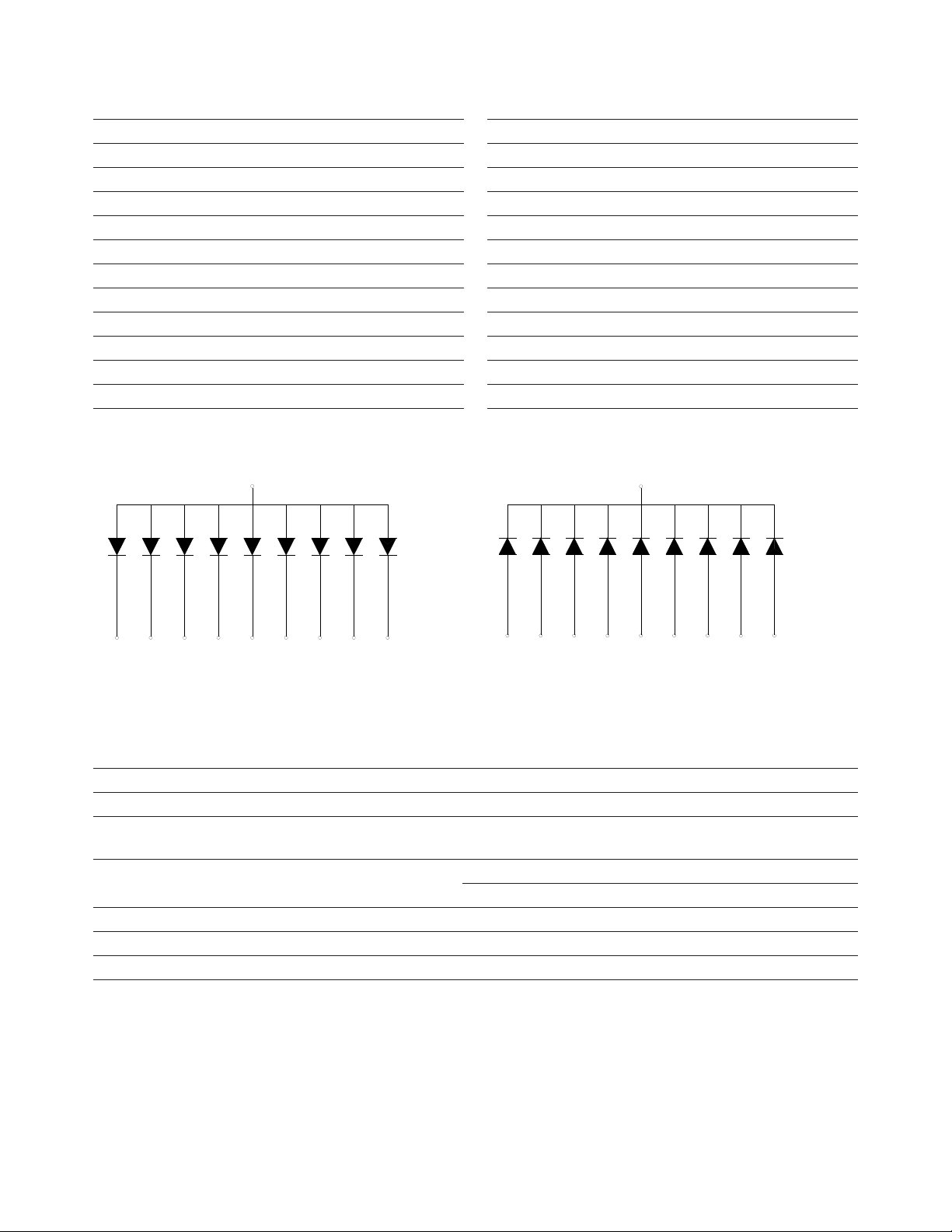
Pin Connection (Common Anode)
4,9
A B C
D
E
F
G DP1
DP2
5
6
8 10
11
3 1 2 7
4,9
A B C
D
E
F
G DP1
DP2
5
6
8 10
11
3 1 2 7
Pin Connection (Common Cathode)
PIN No Connection
1 CATHODE G
2 CATHODE DP1
3 CATHODE F
4 COMMON ANODE
5 CATHODE A
6 CATHODE B
7 CATHODE DP2
8 CATHODE C
9 COMMON ANODE
10 CATHODE D
11 CATHODE E
Internal Circuit Diagram (Common Anode)
PIN No Connection
1 ANODE G
2 ANODE DP1
3 ANODE F
4 COMMON CATHODE
5 ANODE A
6 ANODE B
7 ANODE DP2
8 ANODE C
9 COMMON CATHODE
10 ANODE D
11 ANODE E
Internal Circuit Diagram (Common Cathode)
Absolute Maximum Ratings @ TA=25°
Parameter Green/Yellow/Red/Orange Unit
Power Dissipation Per Segment 65 mW
Peak Forward Current Per Segment
( 1/10 Duty Cycle. ,0.1ms pulse width)
Continuous Forward Current Per Segment
Derating Linear From 25°C Per Segment
Reverse Voltage Per Segment 5 V
Operating Temperature Range -40°C to +105°C
Storage Temperature Range -40°C to +105°C
2
100 mA
25 mA
0.25 mA/ °C
Page 3

Electrical / Optical Characteristics @ TA=25°C
Green
Parameters Symbol Min Typ Max Unit Test Condition
Average Luminous Intensity I
Emissions Wavelength
Spectral Line Half-Width
Forward Voltage, Per Segment V
Reverse Current, Per Segment I
Luminous Intensity Matching Ratio I
V
hp/l
Dl
F
R
V-M
d
Yellow
Parameters Symbol Min Typ Max Unit Test Condition
Average Luminous Intensity I
Emissions Wavelength
Spectral Line Half-Width
Forward Voltage, Per Segment V
Reverse Current, Per Segment I
Luminous Intensity Matching Ratio I
V
lp/l
Dl
F
R
V-M
d
3.4 6 - mcd IF = 10mA
- 572/571 - nm IF = 20mA
- 20 - nm IF = 20mA
- 2.1 2.6 V IF = 20mA
- 100
mA
VR = 5V
- - 2:1 - IF = 10mA
3.4 8.0 - mcd IF = 10mA
- 591/589 - nm IF = 20mA
- 15 - nm IF = 20mA
- 2.1 2.6 V IF = 20mA
- 100
mA
VR = 5V
- - 2:1 - IF = 10mA
Red
Parameters Symbol Min Typ Max Unit Test Condition
Average Luminous Intensity I
Emissions Wavelength
Spectral Line Half-Width
Forward Voltage, Per Segment V
Reverse Current, Per Segment I
Luminous Intensity Matching Ratio I
V
lp/l
Dl
F
R
V-M
d
3.4 7.5 - mcd IF = 10mA
- 632/624 - mm IF = 20mA
- 20 - nm IF = 20mA
- 2.0 2.6 V IF = 20mA
- 100
mA
VR = 5V
- - 2:1 - IF = 10mA
Orange
Parameters Symbol Min Typ Max Unit Test Condition
Average Luminous Intensity I
Emissions Wavelength
Spectral Line Half-Width
Forward Voltage, Per Segment V
Reverse Current, Per Segment I
Luminous Intensity Matching Ratio I
V
lp/l
Dl
F
R
V-M
d
3.4 8.5 - mcd IF = 10mA
- 611/605 - nm IF = 20mA
- 20 - nm IF = 20mA
- 2.1 2.6 V IF = 20mA
- 100
mA
VR = 5V
- - 2:1 - IF = 10mA
3
Page 4

Typical Electrical / Optical characteristic curves @ TA=25°C°C
80
2 0
0
0
1 0
40
2010
30 6050 70
3 0
4 0
0
400
0.5
1.0.
1
20
90
1.2
10
0
0 5
10
15 20 25
30
40
45
30 35 40 50
1.6
2.0 2.4 2.8 3.2
550
2
3
4
450 500 600 650 700
100 110
RELATIVE LUMINOUS INTENSITY
RELATIVE LUMINOUS INTENSITY
WAVELENGTH(nm)
(NORMALIZED TO 1 AT 10MA)
FORWARD CURRENT IF(mA)
FORWARD CURRENT I
F
(mA)
FORWARD CURRENT I
F
(mA)
FORWARD VOLTAGE(V)
AMBIENT TEMPERATURE(°C)
.
0
G
G
G
G
Green
Figure 1. Relative Luminous Intensity vs. Wavelength Figure 2. Relative Luminous Intensity vs. Forward Current
Figure 3. Allowable DC Current vs. Ambient Temperature
Figure 4. Forward Current vs. Forward Voltage
4
Page 5

Yellow
1.0
0.5
0
30
20
10
40
0
0
20
10
30
40
4
0
1
2
3
RELATIVE INTENSITY
RELATIVE INTENSITY
WAVELENGTH(nm)
(NORMALIZED TO 1 AT 10mA)
FORWARD CURRENT IF(mA)
FORWARD CURRENT I
F
(mA)
FORWARD CURRENT I
F
(mA)
FORWARD VOLTAGE(V)
AMBIENT TEMPERATURE(°C)
400
1.0
0 5
10
15 20 254530 35 40 50
1.5
2.0 2.5 3.0 3.5
550450 500 600 650 700
80
0
40
2010
30 6050 70 90 100 110
Figure 1. Relative Intensity vs. Wavelength Figure 2. Relative Intensity vs. Forward Current
Figure 3. Allowable DC Current vs. Ambient Temperature
Figure 4. Forward Current vs. Forward Voltage
5
Page 6

Red
1.0
0.5
0
4
0
1
2
3
RELATIVE LUMINOUS INTENSITY
WAVELENGTH(nm)
(NORMALIZED TO 1 AT 10mA)
FORWARD CURRENT IF(mA)
FORWARD CURRENT I
F
(mA)
FORWARD CURRENT I
F
(mA)
FORWARD VOLTAGE(V)
400
0 5
10
15 20 254530 35 40 50
550450 500 600 650 700
80
20
0
0
10
40
2010
30 6050 70
30
40
90 100 110
20
1.2
10
30
40
1.6
2.0 2.4 2.8 3.2
0
R
R
R
R
RELATIVE LUMINOUS INTENSITY
Figure 1. Relative Luminous Intensity vs. Wavelength Figure 2. Relative Luminous Intensity vs. Forward Current
Figure 3. Allowable DC Current vs. Ambient Temperature
Figure 4. Forward Current vs. Forward Voltage
6
Page 7

Orange
100 105
1.0
0.5
0
10
20
30
40
0
0
20
10
30
40
4
0
1
2
3
RELATIVE INTENSITY
WAVELENGTH(nm)
(NORMALIZED TO 1 AT 10mA)
FORWARD CURRENT IF(mA)
FORWARD CURRENT I
F
(mA)
FORWARD CURRENT I
F
(mA)
FORWARD VOLTAGE(V)
AMBIENT TEMPERATURE(°C)
0
40
2010
30 6050 70
1.0
0 5
10
15 20 254530 35 40 50
1.5
2.0 2.5 3.0 3.5
550450 500 600 650 700 750
80 90
RELATIVE INTENSITY
Figure 1. Relative Intensity vs. Wavelength Figure 2. Relative Intensity vs. Forward Current
Figure 3. Allowable DC Current vs. Ambient Temperature
Figure 4. Forward Current vs. Forward Voltage
7
Page 8

Intensity Bin Limits (mcd)
1.1
3.0
9.8
217 °C
200 °C
60 - 120 SEC.
6 °C/SEC. MAX.
150 °C
255 - 260 °C
100 SEC. MAX.
(Acc. to J-STD-020C)
10 to 30 SEC.
TIME
TEMPERATURE
3 °C/SEC. MAX.
3 °C/SEC. MAX.
Green
IV Bin Category Min. Max.
L 3.401 5.400
M 5.401 8.600
Tolerance: ±15%
Notes:
1. Bin categories are established for classication of products. Products
may not be available in all categories. Please contact your Avago
representative for information on currently available bins.
SMT Soldering Prole
Pb free reow soldering Prole
Yellow / Red / Orange
IV Bin Category Min. Max.
L 3.401 5.400
M 5.401 8.600
N 8.601 13.700
Tolerance: ±15%
Recommended soldering pattern (unit: mm)
Notes:
Number of reow process shall be less than 2 times and cooling process
to normal temperature is required between the rst and than second
soldering process.
8
Page 9

Tape specication (unit: mm)
Tape
24
+0.3
-0.1
1.75 ± 0.1
4 ± 0.1
2 ± 0.1
11.5 ± 0.1
12 ± 0.1
TOP TAPE
1.5
+0.1
-0
0.35 TYP
3.95 ± 0.1
For product information and a complete list of distributors, please go to our web site: www.avagotech.com
Avago, Avago Technologies, and the A logo are trademarks of Avago Technologies Limited in the United States and other countries.
Data subject to change. Copyright © 2008 Avago Technologies Limited. All rights reserved.
AV02-0980EN - February 13, 2008
 Loading...