

Page 1

®
HDP01-0512N
Appl icat ion Sp ecif ic Dis cret es
A.S.D.
APPLICATIONS
PROTECTION FOR THE +5V AND +12V
POWER LINE S OF :
- Hard disk drives
- Floppy disk drives
- CD-ROMs, CD-R, CD-RW
- DVDs
FEATURES
PROTECTION OF BOTH 5V AND 12V SUPPLY
RAILS.
MAXIMUM CURRENT ON THE 5V LINE 3A
DURING 1s.
MONOLITHIC INTEGRATION IN PLANAR
TECHNOLOGY.
DESCR IPT ION
This device is dedicated to the protect ion of the
+5V power supply line against transient overvoltages due to surge of power rails up to the activation of the serial t hermal protection element. It is
also dedicated to the protection of the +12V rail
against transient overvoltages.
TM
HARD DISK DRIVE
POWER SUPPLY PROTECTION
PL5
GND
PL5
PL12
SOT223
BENEFITS
COMPONENT C OUNT RE DUC TION
PCB SURFACE REDUCTION
SIMPLIFIED SYSTEM PROTECTION DESIGN
BASIC APPLICATION DIAGRAM
Unprotected 5V
Unprotected 12V
PL12 PL5
HDP01-0512N
note: The element in series with the 5V line is a resettable device, like Raychem Polyswitch MiniSMD075.
TM
: ASD is trademark of STMicroelectronics.
April 1999 - Ed: 6A
Protected 5V
Protected 12V
Gnd
PL12
OVERVOLTAGE
CLAMPING
PL5
OVERVOLTAGE
DETECTION
1/6
Page 2
HDP01-0512N
ABSOLUTE MAXIMUM RATINGS
Symbol Parameter Value Unit
t
on
T
op
T
T
stg
T
L
note 1 : I-
Conduction time with IOperating temperature range
Maximum junction temperature
j
Storage temperature range
Lead solder temperature (10s dur ation)
is the current going through the 5V line (PL5)
PL5
THERMAL RES IST ANCE
Symbol Parameter Value Unit
Rth (j-t)
Rth (j-a)
note 2 : With 5cm2 copper (e=35µm) surface under tab.
Junction to tab
Junction to ambient (note 2)
ELECTRICAL CHARACTERISTICS (Tamb=25°C)
= 3A DC (note1)
PL5
1s
0 to + 75 ° C
125 ° C
- 55 to + 150 ° C
260 ° C
30
60
°
C/W
°
C/W
I
+5V PROTECTION
ION
IA-PL5
(T
VA-PL5
amb
IRM-PL5
VON-PL5
VRM-PL5
VNA-PL5
ELECTRICAL CHARACTERISTICS
PROTECTION OF 5 V LINE (PL5)
Symbol Parameter
V
-PL5
NA
-PL5
V
A
IRM-PL5
IA-PL5
-PL5
V
ON
Non activation voltage between PL5 and Gn d at IRM=100µA
Activation voltage between PL5 and Gnd
Leakage current between PL5 and Gnd at VRM =5V
Activation current between PL5 and Gnd
Voltage drop on active state at ION=3A
= 25° C)
IRM-PL12
I
+12V PROTECTION
VRM-PL12 VBR-PL12
Value
Min. Typ. Max.
6.0 V
Slope = 1 / Rd
Unit
7.0 7.4 V
1
µ
10 mA
1.3 V
A
PROTECTION OF 12 V LINE (PL12)
Symbol Parameter
Breakdown voltage at IR=1mA
Leakage current between PL12 and Gnd at VRM =12V
Dynamic resistance. Square pulse Ipp=3A, tp = 2.5µ s
2/6
V
I
BR
RM
-PL12
-PL12
Rd
Value
Min. Typ. Max.
14 16 V
1
2.5
Unit
µ
A
Ω
Page 3

HDP01-0512N
Fig. 1:
Non repetitive surge peak on-state current
versus pulse duration (rectangular w aveform).
ITSM(A)
50
10
Pl5 vs GND
Tj initial=25°C
tp(ms)
1
1 10 100 1000
Fig. 3:
Typical clamping voltage versus peak pulse
current (rectangular waveform, tp=2.5µs).
Ipp(A)
3
2
1
0.5
PL12 vs GND
0.1
15 16 17 18 19 20 21 22
Vcl(V)
Fig. 2:
Peak pulse power dissipation versus
exponential pulse duration (Tj initial = 25°C).
Ppp(W)
500
100
10
Pl12 vs GND
1
0.01 0.1 1 10 100 300
Fig. 4:
Thermal resistance junction to ambient
tp(ms)
Tj initial=25°C
versus copper surface under tab (Epoxy printed
circuit board FR4, copper thickness: 35µm).
Rth(j-a) (°C/W)
130
120
110
100
90
80
70
60
50
40
30
20
10
0
012345
S(Cu) (cm²)
Fig. 5:
Thermal impedance junction to ambient
and junction to tab versus pulse duration.
Zth(°C/W)
2E+2
1E+2
1E+1
1E+0
1E-1
1E-2
1E-4 1E-3 1E-2 1E-1 1E+0 1E+1 1E+2
tp(s)
Zth(j-a)
Zth(j-t)
Note:
Rth(j-a) = (Tj
Max
- T
amb
) / P
Max
3/6
Page 4

HDP01-0512N
APPLICATION INFORMATION
DESCR IPT ION
The HDP01-0512N has been specially designed to protect equipment supplied by both +5 and +12 Volt
power rails such as hard disk drives, CD-ROMs, DVDs, floppy disk drives with the topology indicated in
figure A.1.
Fig. A.1:
+12V supply rail
typical application schematic.
This protection device is able to protect both +5 and
+12 Volts power rails against transients and rails in-
ELECTRONIC
MODULE
(i.e. Disk drive)
version.
The internal +5V protection is achieved with a crowbar
structure whereas the +12V one is secured by a
clamping structure.
+5V supply rail
ELIMINATOR
OVERVOLTAGE
HDP01-512N
DETECTOR
OVERVOLTAGE
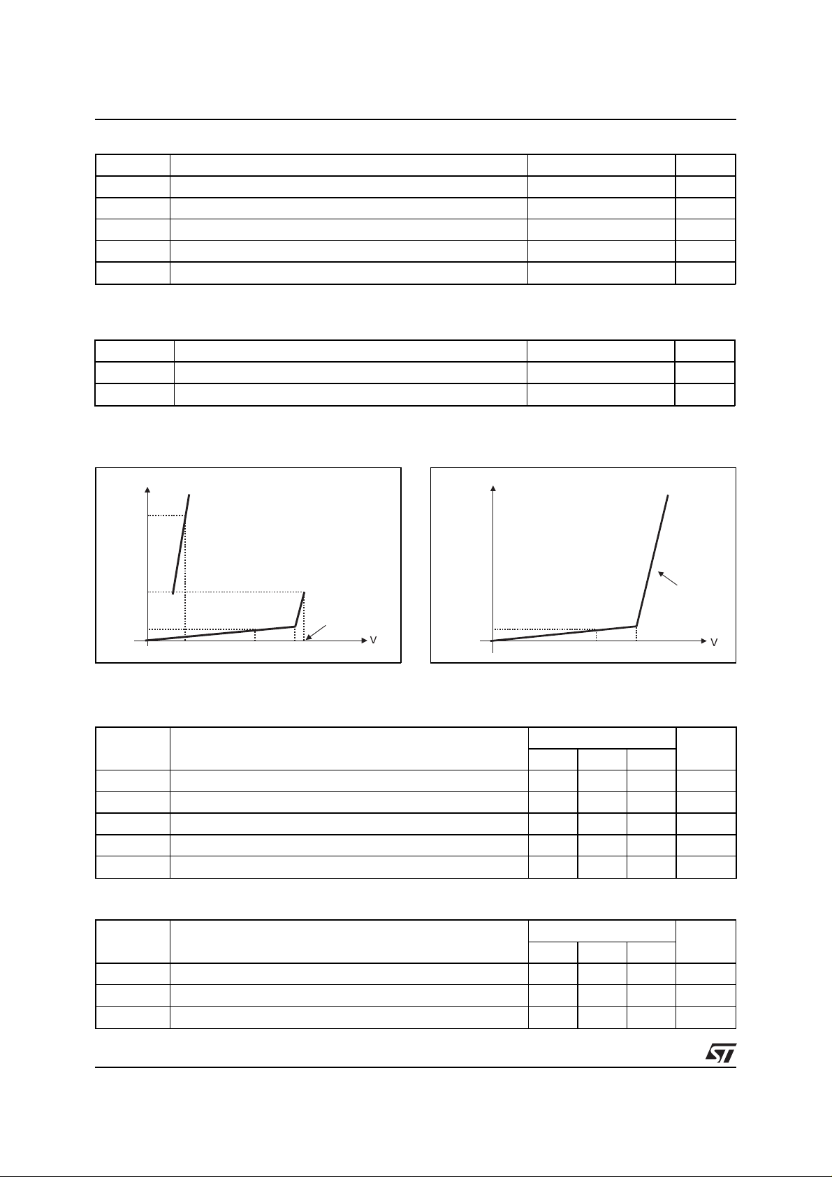
ABOUT THE +5V PROTECTION
In normal conditions, (r egion ➊ of figure A.2) the +5V protection (PL5 termination) of the HDP01-0512N
connected to the +5V rail, is in idle state and its leakage current is 1µA max at +5V @ 25°C. Upon occurrence of transients, the HDP01-0512N eliminates the overvoltage by clamping up to a maximum of +7.4V
(region ➋ ) since the current induced by the transient does not exceed the activation current I
If the I
min current value is passed, the internal +5V protection trips in crowbar mode (region ➌ ) and then
A
min (10mA).
A
a short circuit appears on the +5V rail .
Fig. A.2:
Current and voltage characteristic of the
+5V protection.
I
3
I
H
I
A
1
2
The arrows indicate the way the device is activated
from point ➋ to point ➌ , and the way it goes back in
idle state, point ➌ to point
➊
Thanks to this behavior the electronic module (i.e.
disk drive) connected to the +5V rail is safe.
V
V
A
As soon as the transient disappears and assuming that the current in the +5V power s upply rail is under the
holding current I
protected electronic module turns back on. As in many cases the current delivered by the +5V power supply
is higher than the I
+5V rail (i.e. resettable fuse), connected before the HDP protection. T his will prevent the HDP01-0512N
from being damaged by an over-rated dissipated power. The choice of the serial protector is led by both
peak current and current duration the HDP01-0512N is able to support. The serial protection shall fulfill the
next condition :
4/6
min value (10mA) of the +5V protection, the HDP01-0512N gets back in idle state and the
H
min current value of the HDP01-0512N, it is necessary to use a serial protection on the
H
2
t serial protection < I
i
@ tp of +5V HDP protection.
TSM
Page 5

HDP01-0512N
The I
value as a function of the pulse duration tp for the HDP01 device is given on the figure 1 of this
TSM
datasheet.
In the case the supply cables of the +12V and +5V are reversed, the +5V (PL5) internal protection of the
HDP01-512N immediately shorts circuits +5V rail and ensures on efficient protection of the electronic module.
ABOUT THE +12V PROTECTION
The +12V internal protection (PL12 termination) eliminates all transients appearing on the +12V supply rail.
In normal conditions (region 4 of figure A.3) its leakage current is 1µA maximum at 12V @ 25°C. When a
surge occurs on the +12V rail, the overvoltage is clamped (region 5) and the electronic module connected
to this rail is protected.
Fig. A.3:
Current and voltage characteristic of the
+12V protection.
I
The clamping voltage (Vcl) is depending on several
5
parameters which are :
- current induced by the transient (Ipp)
- ambient temperature effect (αT)
- breakdown voltage of the protection (V
4
- dynamic resistance of the protection (Rd)
BR
)
V
V
CL
To evaluate the clamping voltage appearing on the +12V rail when a transient occurs, the next formula is
needed :
Vcl = V
I
PP
I
PP
max + Rd*I
BR
PP
with a typical Rd equals to 2.5
is the peak current given by the transient which is :
= (Vtransient - Vcl)/Rs
⇒
Vtransient = peak voltage of the transient
⇒
Rs is the series resistance of the surge generator.
Ω
If, for example, we consider a 50V combined surge 1.2/50µs - 8/20µs, as defined by the standard
IEC1000 -4 -5 , t he V cl is c alculated a s :
Vcl = 16 + 2.5*I
then it comes up with Vcl = 17.9V and I
and IPP = (50 - Vcl) / 42 RS = 42 Ω (generator impedance)
PP
= 0.7A
PP
The impact of the temperature on the clamping voltage can be considered as to be :
Vcl(T°C ) = Vcl(25°C) * (1 + αT(T° C-25°C)) where T° C is the ambient temperature for which the module shall
run.
The HDP01-0512N +12V protection has a power dissipation capability that is given in the figure 2 of this
datasheet named "Peak pulse power versus exponential pulse duration". This figure is necessary to determine if the power involved in the +12V protection does not exceed the maximum power the HDP01 +12V
protection can support. For example, considering the last calculation where Vcl=17.9 and I
peak power is in that case 12.5W (Vcl*I
) for a 20µs exponential surge duration. If we compare this value
PP
=0.7A, the
PP
to the curve of figure 2, t hen we see the dissipated power is much lower than the +12V protection limit
(200W @ 20µs) this tells us the +12V protection of the HDP01-0512N can easily withstand such a 12.5W
surge.
5/6
Page 6

HDP01-0512N
PACKAGE ME CHANICAL D AT A
SOT223 (Plastic)
A
A1
B
e1
D
B1
H
E
e
V
DIMENSIONS
REF.
c
A 1.80 0.071
A1 0.02 0.001
B 0.60 0.70 0.80 0.024 0.027 0.031
B1 2.90 3.00 3.10 0.114 0.118 0.122
c 0.24 0.26 0. 32 0.009 0.010 0.013
D 6.30 6.50 6. 70 0.248 0.256 0.264
e 2.3 0.090
e1 4.6 0.181
E 3.30 3.50 3.70 0.130 0.138 0.146
H 6.70 7.00 7. 30 0.264 0.276 0.287
V 10° max
Millimeter s Inc he s
Min. Typ. Max. Min. Typ. Max.
FOOT PRINT DIMENSIONS
SOT223 (Plastic
)
(in millimeters)
MARKING
Order code Marking Package Weight Packing Base Qty
HDP01-0512NRL HD1 SOT223 0.123 g Tape & reel 1000pcs
Information furnished is believed to be accurate and reliable. However, STMicroelectronics assumes no responsibility for the consequences of
use of such information nor for any infringement of patents or other rights of third parties which may result from its use. No license is granted by
implication or otherwi se un der any pat ent or patent rights of STMic roelec tronics. S pecifications ment ioned in t his publ ication are subject to
change without notice. This publication supersedes and replaces all information previously supplied.
STMicroelectronics products are not authorized for use as critical components in li fe s upport devices or systems wi thout express writte n approval of STMicroelectronics.
The ST logo is a registered trademark of STMicroe lectronics
© 1999 STMicroelectronics - Printed in Italy - All rights reser ved.
STMicroelectronics GROUP OF COMPANIES
Australia - Brazil - Canada - China - France - Germany - Italy - Japan - Korea - Malaysia - Malta - Mexico - Morocco -
The Netherlands - Singapore - Spain - Sweden - Switzerland - Taiwan - Thailand - United Kingdom - U.S.A.
http://www.st.com
6/6
 Loading...