

Page 1
Fibre Channel Transceiver Chip
Technical Data
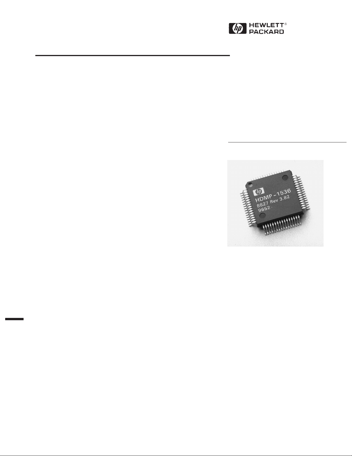
HDMP-1536 Transceiver
HDMP-1546 Transceiver
Features
• ANSI X3.230-1994 Fibre
Channel Compatible (FC-0)
• Supports Full Speed
(1062.5 MBd) Fibre Channel
• Compatible with “Fibre
Channel 10-Bit Interface”
Specification
• Low Power Consumption,
630 mW
• Transmitter and Receiver
Functions Incorporated onto
a Single IC
• Auto Frequency Lock
• Small Package Profile
HDMP-1536, 10x10 mm QFP
HDMP-1546, 14x14 mm QFP
• 10-Bit Wide Parallel TTL
Compatible I/Os
• Single +3.3 V Power Supply
Applications
• 1062.5 MBd Fibre Channel
Interface
• FC Interface for Disk Drives
and Arrays
• Mass Storage System I/O
Channel
• Work Station/Server I/O
Channel
• High Speed Proprietary
Interface
• High Speed Backplane
Interface
Description
The HDMP-1536/46 transceiver
is a single silicon bipolar
integrated circuit packaged in a
plastic QFP package. It provides
a low-cost, low-power physical
layer solution for 1062.5 MBd
Fibre Channel or proprietary link
interfaces. It provides complete
FC-0 functionality for copper
transmission, incorporating both
the Fibre Channel FC-0 transmit
and receive functions into a
single device.
This chip is used to build a highspeed interface (as shown in
Figure 1) while minimizing board
space, power, and cost. It is
compatible with both the ANSI
X3.230-1994/AM 1 - 1996
document and the “Fibre Channel
10-bit Interface” specification.
The transmitter section accepts
10-bit wide parallel TTL data and
multiplexes this data into a highspeed serial data stream. The
parallel data is expected to be
8B/10B encoded data, or
equivalent. This parallel data is
latched into the input register of
the transmitter section on the
rising edge of the 106.25 MHz
reference clock (used as the
transmit byte clock).
The transmitter section’s PLL
locks to this user supplied 106.25
MHz byte clock. This clock is
then multiplied by 10, to generate
the 1062.5 MHz serial signal
clock used to generate the highspeed output. The high-speed
outputs are capable of interfacing
directly to copper cables for
electrical transmission or to a
separate fiber-optic module for
optical transmission.
The receiver section accepts a
serial electrical data stream at
1062.5 MBd and recovers the
original 10-bit wide parallel data.
The receiver PLL locks onto the
incoming serial signal and
recovers the high-speed serial
clock and data. The serial data is
696
5965-8113E (4/97)
Page 2
HDMP-15x6
PROTOCOL DEVICE
BYTSYNC
REFCLK
ENBYTSYNC
-LCKREF
Figure 1. Typical Application Using the HDMP-15x6.
DATA BYTE
TX[0-9]
INPUT
LATCH
FRAME
MUX
TRANSMITTER SECTION
PLL
PLL
RECEIVER SECTION
OUTPUT
SELECT
SERIAL DATA OUT
SERIAL DATA IN
± DOUT
TXCAP0
TXCAP1
REFCLK
-LCKREF
RXCAP0
RXCAP1
RBC0
RBC1
DATA BYTE
RX[0-9]
TX
PLL/CLOCK
GENERATOR
FRAME
DEMUX
DRIVER
OUTPUT
BYTE SYNC
BYTSYNC ENBYTSYNC
AND
INTERNAL
TX CLOCKS
Figure 2. HDMP-15x6 Transceiver Block Diagram.
RX
PLL/CLOCK
RECOVERY
RX CLOCKS
INPUT
SAMPLER
INTERNAL
LOOPBACK
INTERNAL
INPUT
SELECT
LOOPEN
± DIN
697
Page 3

converted back into 10-bit
parallel data, recognizing the
8B/10B comma character to
establish byte alignment.
The recovered parallel data is
presented to the user at TTL
compatible outputs. The receiver
section also recovers two
53.125 MHz receiver byte clocks
that are 180 degrees out of phase
with each other. The parallel data
is properly aligned with the rising
edge of alternating clocks.
The transceiver provides for onchip local loop-back functionality,
controlled through an external
input pin. Additionally, the byte
synchronization feature may be
disabled. This may be useful in
proprietary applications which
use alternative methods to align
the parallel data.
HDMP-1536/46 Block Diagram
The HDMP-1536/46 was designed
to transmit and receive 10-bit
wide parallel data over a single
high-speed line, as specified for
the FC-0 layer of the Fibre
Channel standard. The parallel
data applied to the transmitter is
expected to be encoded per the
Fibre Channel specification,
which uses an 8B/10B encoding
scheme with special reserve
characters for link management
purposes. In order to accomplish
this task, the HDMP-1536/46
incorporates the following:
• TTL Parallel I/Os
• High Speed Phase Lock Loops
• Clock Generation/Recovery
Circuitry
• Parallel to Serial Converter
• High-Speed Serial Clock and
Data Recovery Circuitry
• Comma Character Recognition
Circuitry
• Byte Alignment Circuitry
• Serial to Parallel Converter
INPUT LATCH
The transmitter accepts 10-bit
wide TTL parallel data at inputs
TX[0..9]. The user-provided
reference clock signal, REFCLK,
is also used as the transmit byte
clock. The TX[0..9] and REFCLK
signals must be properly aligned,
as shown in Figure 3.
TX PLL/CLOCK GENERATOR
The transmitter Phase Lock Loop
and Clock Generator (TX PLL/
CLOCK GENERATOR) block is
responsible for generating all
internal clocks needed by the
transmitter section to perform its
functions. These clocks are based
on the supplied reference byte
clock (REFCLK). REFCLK is used
as both the frequency reference
clock for the PLL and the transmit byte clock for the incoming
data latches. It is expected to be
106.25 MHz and properly aligned
to the incoming parallel data (see
Figure 3). This clock is multiplied
by 10 to generate the 1062.5
MHz clock necessary for the high
speed serial outputs.
FRAME MUX
The FRAME MUX accepts the 10bit wide parallel data from the
INPUT LATCH. Using internally
generated high speed clocks, this
parallel data is multiplexed into
the 1062.5 MBd serial data
stream. The data bits are transmitted sequentially, from the
least significant bit (TX[0]) to the
most significant bit (TX[9]).
OUTPUT SELECT
The OUTPUT SELECT block
provides for an optional internal
loopback of the high speed serial
signal, for testing purposes.
In normal operation, LOOPEN is
set low and the serial data stream
is placed at ± DOUT. When wrapmode is activated by setting
LOOPEN high, the ± DOUT pins
are held static and the serial
output signal is internally
wrapped to the INPUT SELECT
box of the receiver section.
INPUT SELECT
The INPUT SELECT block determines whether the signal at ± DIN
or the internal loop-back serial
signal is used. In normal operation, LOOPEN is set low and the
serial data is accepted at ± DIN.
When LOOPEN is set high, the
high-speed serial signal is
internally looped-back from the
transmitter section to the receiver
section. This feature allows for
loop-back testing exclusive of the
transmission medium.
RX PLL/CLOCK RECOVERY
The RX PLL/CLOCK RECOVERY
block is responsible for frequency
and phase locking onto the
incoming serial data stream and
recovering the bit and byte
clocks. An automatic locking
feature allows the Rx PLL to lock
onto the input data stream
without external controls. It does
this by continually frequency
locking onto the 106.25 MHz
clock, and then phase locking
onto the input data stream. An
internal signal detection circuit
monitors the presence of the
input, and invokes the phase
detection as the data stream
appears. Once bit locked, the
receiver generates the high speed
sampling clock at 1062.5 MHz
for the input sampler, and
recovers the two 53.125 MHz
receiver byte clocks (RBC1/
RBC0). These clocks are 180° out
of phase with each other, and are
698
Page 4

alternately used to clock the 10bit parallel output data.
An optional -LCKREF pin is
available for users who want to
gain full control during the
frequency acquisition process.
Asserting this pin will force the
Rx PLL to fully phase and
frequency lock onto the reference
clock, disregarding the serial
stream completely.
To enable the auto-locking
feature, the -LCKREF pin should
be tied to VCC. The receiver will
detect the absence of high-speed
serial data into +DIN (pin 54)
and -DIN (pin 52) and lock onto
the reference clock (REFCLK).
RBC0 and RBC1 will remain
frequency locked to 53.125 MHz.
The receiver will frequency and
phase lock onto the incoming
valid data once it is reapplied.
INPUT SAMPLER
The INPUT SAMPLER is
responsible for converting the
serial input signal into a re-timed
serial bit stream. In order to
accomplish this, it uses the high
speed serial clock recovered from
the RX PLL/CLOCK RECOVERY
block. This serial bit stream is
sent to the FRAME DEMUX and
BYTE SYNC block.
FRAME DEMUX AND BYTE SYNC
The FRAME DEMUX AND BYTE
SYNC block is responsible for
restoring the 10-bit parallel data
from the high speed serial bit
stream. This block is also
responsible for recognizing the
comma character (or a K28.5
character) of positive disparity
(0011111xxx). When recognized,
the FRAME DEMUX AND BYTE
SYNC block works with the RX
PLL/CLOCK RECOVERY block to
properly align the receive byte
clocks to the parallel data. When
a comma character is detected
and realignment of the receiver
byte clocks (RBC1/RBC0) is
necessary, these clocks are
stretched, not slivered, to the
next possible correct alignment
position. These clocks will be
fully aligned by the start of the
second 4-byte ordered set. The
second comma character received
shall be aligned with the rising
edge of RBC1. Comma characters
should not be transmitted in
consecutive bytes to allow the
receiver byte clocks to maintain
their proper recovered
frequencies.
OUTPUT DRIVERS
The OUTPUT DRIVERS present
the 10-bit parallel recovered data
byte properly aligned to the
receiver byte clocks
(RBC1/RBC0), as shown in
Figure 5. These output data
buffers provide TTL compatible
signals.
Recommended Handling Precautions
Additional circuitry is built into
the various input and output pins
on this chip to protect against
low level electrostatic discharge;
however, they are still ESD
sensitive. Standard procedures
for static sensitive devices should
be used in the handling and
assembly of this product.
699
Page 5

HDMP-1536/46 (Transmitter Section)
Timing Characteristics
[1]
T
= 0°C to +60°C, VCC = 3.15 V to 3.45 V
A
Symbol Parameter Units Min. Typ. Max.
t
setup
t
hold
[2]
t_txlat
Notes:
1. Device tested and characterized under TA conditions specified, with TC monitored at approximately 20° higher than TA.
2. The transmitter latency, as shown in Figure 4, is defined as the time between the latching in of the parallel data word (as triggered
by the rising edge of the transmit byte clock, REFCLK) and the transmission of the first serial bit of that parallel word (defined by
the rising edge of the first bit transmitted).
Setup Time nsec 2
Hold Time nsec 1.5
Transmitter Latency nsec 7.5
bits 8.0
REFCLK
TX[0]-TX[9]
DATA
t
setup
Figure 3. Transmitter Section Timing.
± DOUT
TX[0]-TX[9]
T5 T6 T7 T8 T9 T0 T1 T2 T3 T4 T5 T6 T7 T8 T9 T0 T1 T2 T3 T4 T5
DATA DATA
t
hold
DATA BYTE A
t_txlat
DATA BYTE B DATA BYTE C
DATA DATA
1.4 V
2.0 V
0.8 V
DATA BYTE B
REFCLK
Figure 4. Transmitter Latency.
700
1.4 V
Page 6

HDMP-1536/46 (Receiver Section)
,
Timing Characteristics
[1]
T
= 0°C to +60°C, VCC = 3.15 V to 3.45 V
A
Symbol Parameter Units Min. Typ. Max.
b_sync
Notes:
1. Device tested and characterized under TA conditions specified, with TC monitored at approximately 20° higher than TA.
2. This is the recovery time for input phase jumps, per the FC-PH specification Ref 4.1, Sec 5.3.
3. Tested using C
4. The RBC clock skew is calculated as t
5. The receiver latency, as shown in Figure 6, is defined as the time between receiving the first serial bit of a parallel data word (as
defined as the first edge of the first serial) and the clocking out of that parallel word (defined by the rising edge of the receive byte
clock, either RBC1 or RBC0).
[2,3]
t
valid_before
t
valid_after
t
duty
[4]
t
A-B
[5]
t_rxlat
t
valid_before
= 0.1 µF.
PLL
Bit Sync Time bits 2500
Time Data Valid Before Rising Edge of RBC nsec 3 3.8
Time Data Valid After Rising Edge of RBC nsec 1.5 3.5
RBC Duty Cycle % 40 60
Rising Edge Time Difference nsec 8.9 9.4 9.9
Receiver Latency nsec 24.5
bits 26
A-B(max)
t
valid_after
- t
A-B(min)
.
RBC1
RX[0]-RX[9]
BYTSYNC
RBC0
K28.5
Figure 5. Receiver Section Timing.
DATA BYTE C
R5 R6 R7 R8 R9 R0 R1 R2 R3 R4 R5 R6 R7 R8 R9 R2 R3 R4 R5
± DIN
RX[0]-RX[9]
DATA DATA
DATA BYTE D
t_rxlat
DATA BYTE A DATA BYTE D
DATA DATA
t
1.4 V
2.0 V
0.8 V
2.0 V
0.8 V
1.4 V
A-B
Figure 6. Receiver Latency.
RBC1/0
1.4 V
701
Page 7

Absolute Maximum Ratings
TA = 25°C, except as specified. Operation in excess of any one of these conditions may result in permanent
damage to this device.
Symbol Parameter Units Min. Max.
V
CC
V
IN,TTL
V
IN,HS_IN
I
O,TTL
T
stg
T
j
Supply Voltage V -0.5 5.0
TTL Input Voltage V -0.7 VCC + 0.7
HS_IN Input Voltage V 2.0 V
CC
TTL Output Source Current mA 13
Storage Temperature °C -40 +130
Junction Operating Temperature °C 0 +130
Guaranteed Operating Rates
[1]
T
= 0°C to +60°C, VCC = 3.15 V to 3.45 V
A
Parallel Clock Rate (MHz) Serial Baud Rate (MBaud)
Min. Max. Min. Max.
106.20 106.30 1062.0 1063.0
Note:
1. Device tested and characterized under TA conditions specified, with TC monitored at
approximately 20° higher than TA.
Transceiver Reference Clock Requirements
[1]
T
= 0°C to +60°C, VCC = 3.15 V to 3.45 V
A
Symbol Parameter Unit Min. Typ. Max.
f Nominal Frequency (for Fibre Channel Compliance) MHz 106.20 106.25 106.30
F
tol
Frequency Tolerance ppm -100 +100
Symm Symmetry (Duty Cycle) % 40 60
Note:
1. Device tested and characterized under TA conditions specified, with TC monitored at approximately 20° higher than TA.
DC Electrical Specifications
[1]
T
= 0°C to +60°C, VCC = 3.15 V to 3.45 V
A
Symbol Parameter Unit Min. Typ. Max.
V
IH,TTL
V
IL,TTL
V
OH,TTL
V
OL,TTL
I
IH,TTL
I
IL-TTL
CC,TRx
[2,3]
I
Notes:
1. Device tested and characterized under TA conditions specified, with TC monitored at approximately 20° higher than TA.
2. Measurement Conditions: Tested sending 1062.5 MBd PRBS 27-1 sequence from a serial BERT with both DOUT outputs biased
with 150 Ω resistors.
3. Typical specified with VCC = 3.3 volts, maximum specified with VCC = 3.45 volts.
TTL Input High Voltage Level, Guaranteed High Signal V 2 V
for All Inputs
TTL Input Low Voltage Level, Guaranteed Low Signal for V 0 0.8
All Inputs
TTL Output High Voltage Level, IOH = -400 µA V 2.2 V
TTL Output Low Voltage Level, IOL = 1 mA V 0 0.6
Input High Current (Magnitude), VIN = V
CC
µA 0.004 40
Input Low Current (Magnitude), VIN = 0 Volts µA -325 -600
Transceiver VCC Supply Current, TA = 25°C mA 220
CC
CC
702
Page 8

AC Electrical Specifications
[1]
T
= 0°C to +60°C, VCC = 3.15 V to 3.45 V
A
Symbol Parameter Units Min. Typ. Max.
t
r,TTLin
t
f,TTLin
t
r,TTLout
t
f,TTLout
t
rs,HS_OUT
t
fs,HS_OUT
t
rd,HS_OUT
t
fd,HS_OUT
V
IP,HS_IN
V
OP,HS_OUT
Notes:
1. Device tested and characterized under TA conditions specified, with TC monitored at approximately 20° higher than TA.
2. Output Peak-to-Peak Differential Voltage specified as DOUT+ minus DOUT-.
[2]
Input TTL Rise Time, 0.8 to 2.0 Volts nsec 2
Input TTL Fall Time, 2.0 to 0.8 Volts nsec 2
Output TTL Rise Time, 0.8 to 2.0 Volts, 10 pF Load nsec 1.5 2.4
Output TTL Fall Time, 2.0 to 0.8 Volts, 10 pF Load nsec 1.1 2.4
HS_OUT Single-Ended (+DOUT) Rise Time psec 255 375
HS_OUT Single-Ended (+DOUT) Fall Time psec 185 375
HS_OUT Differential Rise Time psec 255
HS_OUT Differential Fall Time psec 185
HS_IN Input Peak-to-Peak Differential Voltage mV 200 1200 2000
HS_OUT Output Peak-to-Peak Differential Voltage mV 1200 1600 2200
22.0680 ns200.0 ps/div
a. Differential HS_OUT Output (Dout+ Minus Dout-).
22.0680 ns200.0 ps/div
b. Single-Ended HS_OUT Output (Dout+).
Eye Diagrams of the High-Speed Serial Outputs from the HDMP-1536/46
as Captured on the HP 83480A Digital Communications Analyzer. Tested with PRBS = 27-1.
Figure 7. Transmitter DOUT Eye Diagrams.
Yaxis = 400 mV/DIV
Yaxis = 200 mV/DIV
703
Page 9

Output Jitter Characteristics
TA = 25°C, VCC = 3.3 V
Symbol Parameter Units Typ.
[1]
RJ
[1]
DJ
Note:
1. Defined by Fibre Channel Specification Rev 4.1, Annex A, Section A.4 and tested using measurement method shown in Figure 8.
Random Jitter at DOUT, the High Speed Electrical Data Port, specified as ps 8
1 sigma deviation of the 50% crossing point (RMS)
Deterministic Jitter at DOUT, the High Speed Electrical Data Port (pk-pk) ps 15
HP70841B
PATTERN
GENERATOR
+K28.5, -K28.5
+ DATA
- DATA
HP83480A
OSCILLOSCOPE
TRIGGER
CH1 CH2
+DOUT -DOUT
HDMP-1636
REFCLK LOOPEN
Tx[0..9]
ENBYTSYNC
Rx[0..9]
HP70841B
PATTERN
GENERATOR*
0000011111
1.0625 GHz
HP70311A
CLOCK SOURCE
* PATTERN
GENERATOR
PROVIDES A
DIVIDE BY
10 FUNCTION.
+ DATA
- DATA
106.25 MHz
BIAS
TEE
1.4 V
HP83480A
OSCILLOSCOPE
TRIGGER
CH1 CH2
+DOUT -DOUT
HDMP-1536
REFCLK
LOOPEN
Tx[0..9]
0011111000
(STATIC K28.7)
DIVIDE
BY 10
CIRCUIT
(DUAL
OUTPUT)
VARIABLE
DELAY
TTL
HP70311A
CLOCK SOURCE
1.25 GHz
DIVIDE
BY 2
CIRCUIT
125 MHz
a. Block Diagram of RJ Measurement Method. b. Block Diagram of DJ Measurement Method.
Figure 8. Transmitter Jitter Measurement Method.
-DIN
+DIN
Thermal and Power Temperature Characteristics,
[1]
T
= 0°C to +60°C, VCC = 3.15 V to 3.45 V
A
Symbol Parameter Units Typ. Max.
[2,3]
P
D,TRx
[2,3,4]
P
D,TRx
[5]
Θ
jc
Notes:
1. Device tested and characterized under TA conditions specified, with TC monitored at approximately 20° higher than TA.
2. PD is multiplying the max VCC by the max ICC and subtracting the power dissipated outside the chip at the high speed bias resistors.
3. Typical specified with VCC = 3.3 volts, maximum specified with VCC = 3.45 volts.
4. Specified with high speed outputs biased with 150 Ω resistors and receiver TTL outputs driving 10 pF loads.
5. Based on independant package testing by HP. Θja for these devices is 48°C/Watt for the HDMP-1536 and 44°C/Watt for the
HDMP-1546. Θja is measured on a standard 3x3" FR4 PCB in a still air environment. To determine the actual junction temperature
in a given application, use the value as described as follows: Tj = TC + (Θjc x Pd), where TC is the case temperature measured on
the top center of the package and PD is the power being dissipated.
704
Transceiver Power Dissipation, Outputs Open, Parallel Data mW 630 850
has 5 Ones and 5 Zeroes
Transceiver Power Dissipation, Outputs Connected per mW 685 900
Recommended Bias Terminations with Idle Pattern
Thermal Resistance, Junction to Case HDMP-1536 °C/Watt 10
HDMP-1546 7
Page 10

I/O Type Definitions
I/O Type Definition
I-TTL Input TTL, Floats High When Left Open
O-TTL Output TTL
HS_OUT High Speed Output, ECL Compatible
HS_IN High Speed Input
C External Circuit Node
S Power Supply or Ground
Pin Input Capacitance
Symbol Parameter Units Typ. Max.
C
INPUT
O_TTL I_TTL
V
_TTL
CC
Input Capacitance on TTL Input Pins pF 1.6
VCC_TTL
RR
GND_TTL
R
ESD
PROTECTION
VCC_TX
or
V
_RX
CC
GND
PROTECTION
Figure 9. O-TTL and I-TTL Simplified Circuit Schematic.
HS_OUT
VCC_TXHS
VCC_TXECL
VCC_TX
+DOUT
R
PAD
150
R
PAD
GND_TXHS
ESD
PROTECTION
-DOUT
GND
150
ESD
Zo = 75 Ω
Zo = 75 Ω
R
GND_TTL
VCC_RXHS
VCC_RX
0.01
150
0.01
GND
GND_RXHS
+DIN
-DIN
R
ESD
PROTECTION
V
1.4 V
BB
HS_IN
+
–
+
–
R
R
Figure 10. HS_OUT and HS_IN Simplified Circuit Schematic.
Notes:
1. HS_IN inputs should never be connected to ground as permanent damage to the device may result.
2. The optional series padding resistors (Rpad) help dampen load reflections. Typical Rpad values for mismatched loads range
between 25-75 Ω.
705
Page 11

_TXHS
CC
GND_TXHS
V
+DOUT
_TXECL
CC
-DOUT
V
_TX
CC
V
GND
_RX
V
_RXHS
CC
CC
GND_RXHS
V
+DIN
_RXHS
CC
V
-DIN
_RXA
CC
GND_RXA
V
RXCAP1
GND_TXTTL
TX[0]
TX[1]
TX[2]
V
_TXTTL
CC
TX[3]
TX[4]
TX[5]
TX[6]
V
_TXTTL
CC
TX[7]
TX[8]
TX[9]
GND_TXTTL
GND_TXA
TXCAP1
64 63 62 61 60 59 58 57 56 55 54 53 52 51 50 49
1
2
3
4
5
6
7
8
9
10
11
12
13
14
15
16
17 18 19 20 21 22 23 24 25 26 27 28 29 30 31 32
_TXA
CC
TXCAP0
V
xxxx-x = WAFER LOT NUMBER–BUILD NUMBER
Rzz.zz = DIE REVISION
S = SUPPLIER CODE
YYWW = DATE CODE (YY = YEAR, WW = WORK WEEK)
COUNTRY = COUNTRY OF MANUFACTURE
(MARKED ON BACK OF DEVICE)
HDMP-15x6
xxxx-x Rz.zz
S YYWW
_TX
V
LOOPEN
CC
GND
_RX
CC
V
REFCLK
*N/C
GND
-LCKREF
ENBYTSYNC
_RX
CC
V
_RXTTL
CC
V
RBC1
RBC0
48
47
46
45
44
43
42
41
40
39
38
37
36
35
34
33
GND_RXTTL
RXCAP0
BYTSYNC
GND_RXTTL
RX[0]
RX[1]
RX[2]
V
_RXTTL
CC
RX[3]
RX[4]
RX[5]
RX[6]
V
_RXTTL
CC
RX[7]
RX[8]
RX[9]
GND_RXTTL
Figure 11. HDMP-1536/46 (TRx) Package Layout and Marking, Top View.
*Note: Pin 26 is designated as a “no connect” pin and should be left unconnected.
706
Page 12

TRx I/O Definition
Name Pin Type Signal
BYTSYNC 47 O-TTL Byte Sync Output: An active high output. Used to indicate detection of
either a comma character or a K28.5 special character (0011111XXX). It
is only active when ENBYTSYNC is enabled.
-DIN 52 HS_IN Serial Data Inputs: High-speed inputs. Serial data is accepted from the
+DIN 54 ± DIN inputs when LOOPEN is low.
-DOUT 61 HS_OUT Serial Data Outputs: High-speed outputs. These lines are active when
+DOUT 62 LOOPEN is set low. When LOOPEN is set high, these outputs are held
static.
ENBYTSYNC 24 I-TTL Enable Byte Sync Input: When high, turns on the internal byte sync
function to allow clock synchronization to a comma character, or a
K28.5 character (0011111XXX). When the line is low, the function is disabled and will not reset registers and clocks, or strobe the BYTSYNC line.
GND 21 S Logic Ground: Normally 0 volts. This ground is used for internal PECL
25 logic. It should be isolated from the noisy TTL ground as well as possible.
58
GND_RXA 51 S Analog Ground: Normally 0 volts. Used to provide a clean ground
plane for the receiver PLL and high-speed analog cells.
GND_RXHS 56 S Ground: Normally 0 volts.
GND_RXTTL 32 S TTL Receiver Ground: Normally 0 volts. Used for the TTL output cells
33 of the receiver section.
46
GND_TXA 15 S Analog Ground: Normally 0 volts. Used to provide a clean ground plane
for the PLL and high-speed analog cells.
GND_TXHS 64 S Ground: Normally 0 volts.
GND_TXTTL 1 S TTL Transmitter Ground: Normally 0 volts. Used for the TTL input cells
14 of the transmitter section.
-LCKREF 27 I-TTL Lock to Reference: When low, causes the PLL to acquire frequency and
phase lock on the external reference, supplied at REFCLK. When high,
the Rx PLL will automatically frequency lock to REFCLK and phase lock
to the high speed data stream.
LOOPEN 19 I-TTL Loopback Enable Input: When set high, the high-speed serial signal is
internally wrapped from the transmitter’s serial loopback outputs back
to the receiver’s loopback inputs. Also, when in loopback mode, the
± DOUT outputs are held static. When set low, ± DOUT outputs and
± DIN inputs are active.
RBC1 30 O-TTL Receiver Byte Clocks: The receiver section recovers two 53.125 MHz
RBC0 31 receive byte clocks. These two clocks are 180 degrees out of phase.
The receiver parallel data outputs are alternatively clocked on the
rising edge of these clocks. The rising edge of RBC1 aligns with the
output of the comma character (for byte alignment) when detected.
REFCLK 22 I-TTL Reference Clock and Transmit Byte Clock: A 106.25 MHz clock
supplied by the host system. The transmitter section accepts this signal
as the frequency reference clock. It is multiplied by 10 to generate the
serial bit clock and other internal clocks. The transmit side also uses this
clock as the transmit byte clock for the incoming parallel data
TX[0]..TX[9]. It also serves as the reference clock for the receive
portion of the transceiver.
707
Page 13

TRx I/O Definition (cont’d.)
Name Pin Type Signal
RX[0] 45 O-TTL Data Outputs: One 10 bit data byte. RX[0] is the first bit received.
RX[1] 44 RX[0] is the least significant bit.
RX[2] 43
RX[3] 41
RX[4] 40
RX[5] 39
RX[6] 38
RX[7] 36
RX[8] 35
RX[9] 34
RXCAP0 48 C Loop Filter Capacitor: A loop filter capacitor for the internal PLL must
RXCAP1 49 be connected across the RXCAP0 and RXCAP1 pins. (typical value = 0.1 µF).
TX[0] 2 I-TTL Data Inputs: One, 10 bit, pre-encoded data byte. TX[0] is the first bit
TX[1] 3 transmitted. TX[0] is the least significant bit.
TX[2] 4
TX[3] 6
TX[4] 7
TX[5] 8
TX[6] 9
TX[7] 11
TX[8] 12
TX[9] 13
TXCAP1 16 C Loop Filter Capacitor: A loop filter capacitor must be connected across
TXCAP0 17 the TXCAP1 and TXCAP0 pins (typical value = 0.1 µF).
VCC_RX 23 S Logic Power Supply: Normally 3.3 volts. Used for internal receiver
28 PECL logic. It should be isolated from the noisy TTL supply as well as
57 possible.
VCC_RXA 50 S Analog Power Supply: Normally 3.3 volts. Used to provide a clean
supply line for the PLL and high-speed analog cells.
VCC_RXHS 53 S High-Speed Supply: Normally 3.3 volts. Used only for the high-speed
55 receiver cell (HS_IN). Noise on this line should be minimized for best
operation.
VCC_RXTTL 29 S TTL Power Supply: Normally 3.3 volts. Used for all TTL receiver output
37 buffer cells.
42
VCC_TX 20 S Logic Power Supply: Normally 3.3 volts. Used for internal transmitter PECL
59 logic. It should be isolated from the noisy TTL supply as well as possible.
VCC_TXA 18 S Analog Power Supply: Normally 3.3 volts. Used to provide a clean
supply line for the PLL and high-speed analog cells.
VCC_TXECL 60 S High-Speed ECL Supply: Normally 3.3 volts. Used only for the last stage
of the high-speed transmitter output cell (HS_OUT) as shown in
Figure 10. Due to high current transitions, this VCC should be well
bypassed to a ground plane.
VCC_TXHS 63 S High-Speed Supply: Normally 3.3 volts. Used by the transmitter side for the
high-speed circuitry. Noise on this line should be minimized for best operation.
VCC_TXTTL 5 S TTL Power Supply: Normally 3.3 volts. Used for all TTL
10 transmitter input buffer cells.
708
Page 14

VCC*
V
CC
users that want full control
during the frequency acquisition
process.
GND_TXTTL
GND_TXHS
_TXTTL
V
CC
_TXHS
CC
V
_TX
CC
V
_TXECL
CC
V
GND
TOP VIEW
_TXTTL
V
CC
GND_TXTTL
GND_TXA
_TX
_TXA
TXCAP1
C
PLLT
* SUPPLY VOLTAGE INTO VCC_RXA AND VCC_TXA SHOULD
BE FROM A LOW NOISE SOURCE. ALL BYPASS CAPACITORS
AND PLL FILTER CAPACITORS ARE 0.1 µF.
Figure 12. Power Supply Bypass.
CC
TXCAP0
V
VCC*
_RX
CC
GND
CC
V
V
Start-up Procedure:
The transceiver start-up
procedure(s) use the following
conditions: VCC = +3.3 V ± 5%
and REFCLK = 106.25 MHz
± 100 ppm.
Auto-Lock Used Exclusively
Set -LCKREF = 1 and apply valid
data using a balanced code such
as 8B/10B. Frequency lock
occurs within 500 µs. After
frequency lock, phase lock occurs
within 2500 bit times.
C
PLLR
_RX
CC
V
GND_RXHS
GND
_RXHS
CC
V
_RXHS
CC
V
V
V
_RXTTL
_RX
CC
CC
V
V
GND_RXA
CC
CC
_RXA
CC
RXCAP1
V
_RXTTL
_RXTTL
GND_RXTTL
RXCAP0
GND_RXTTL
User Controlled
Set -LCKREF = 0 for at least 500
µs (frequency lock will occur
within 500 µs). After valid
8B/10B data is applied to the Rx
input, set -LCKREF=1. Phase
lock will occur within 2500 bit
times. In this case, asserting
-LCKREF = 0 forces the Rx PLL
to fully phase and frequency lock
onto the reference clock
(REFCLK) disregarding the serial
data stream completely. Asserting
-LCKREF = 0 is an option for
GND_RXTTL
Transceiver Power Supply Bypass and Loop Filter Capacitors
Bypass capacitors should be used
and placed as close as possible to
the appropriate power supply
pins of the HDMP-1536/46 as
shown on the schematic of Figure
12. All bypass chip capacitors are
V
CC
0.1 µF. The VCC_RXA and
VCC_TXA pins are the analog
power supply pins for the PLL
sections. The voltage into these
pins should be clean with
minimum noise. The PLL loop
filter capacitors and their pin
locations are also shown on
Figure 12. Notice that only two
capacitors are required: C
the transmitter and C
receiver. Nominal capacitance is
0.1 µF. The voltage across the
capacitors is on the order of 1
volt, so the capacitor can be a
low voltage type and physically
small. The PLL capacitors are
placed physically close to the
appropriate pins on the HDMP1536/46. Keeping the lines short
will prevent them from picking
up stray noise from surrounding
lines or components.
PLLR
for
PLLT
for the
709
Page 15

Package Information
Item Details
Package Material Plastic
Lead Finish Material 85% Tin, 15% Lead
Lead Finish Thickness 300-800 µm
Lead Coplanarity
HDMP-1536 HDMP-1546
0.08 mm max. 0.10 mm max.
Mechanical Dimensions
PIN #1 ID
64 63 62 61 60 59 58 57 56 55 54 53 52 51 50 49
1
2
3
4
5
6
7
8
9
10
11
12
13
14
15
16
HDMP-15x6
TOP VIEW
17 18 19 20 21 22 23 24 25 26 27 28 29 30 31 32
48
47
46
45
44
43
42
41
40
39
38
37
36
35
34
33
A1
A2
B4
A1
A2
C1
B1
B2
B3
C3
C2
B5
Part
Number A1 A2 B1 B2 B3 B4 B5 C1 C2 C3
HDMP-1536 10.00 13.20 0.22 0.50 0.88 0.17 0.25 2.00 0.25 min. 2.45
HDMP-1546 14.00 17.20 0.35 0.80 0.88 0.17 0.25 2.00 0.25 max. 2.35
Tolerance ± 0.10 ± 0.25 ± 0.05 Basic +0.15 max. +0.10/-0.05 max.
-0.10
Figure 13. Mechanical Dimensions of HDMP-1536/46.
710
 Loading...