

Page 1
for High Definition and New Super-Slim CRT Display
Features
■ STATE-OF-THE-ART TECHNOLOGY:
DIFFUSED COLLECTOR “ENHANCED
GENERATION“ EHVS1
■ WIDER RANGE OF OPTIMUM DRIVE
CONDITIONS
■ LESS SENSITIV E TO OPER ATIN G
TEMPERATURE VARIATION
■ FULLY INSULA TED PO WE R PACKA GE
WHICH IS U.L COMPLIANT
HD1530FX
High Voltage NPN Power Transistor
3
2
1
Applications
■ HORIZONTAL DEFLECTION OUTPUT FOR
DIGITAL TV, HDTV, AND HIGH -END
MONITORS
Description
The device uses a Diffused Collector in Planar
technology which adopts ”Enhanced High Voltage
Structure” (EHVS1) that was developed to fit
High-Definition CRT displays.
The new HD product series features improved
silicon efficiency , bringing updated performance to
Horizontal Deflection output stages.
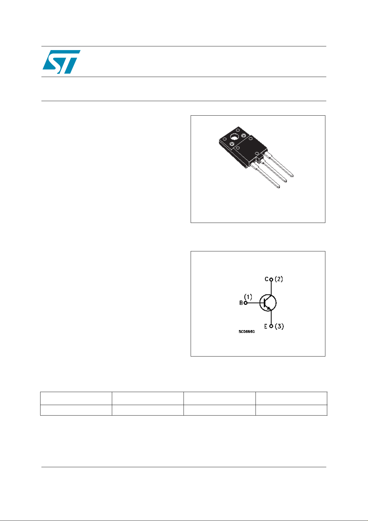
Order Codes
ISOWATT218FX
Internal Schematic Diagram
Part Number Marking Package Packing
HD1530FX HD1530FX ISOWATT218FX TUBE
rev.3
August 2005 1/7
www.st.com
7
Page 2
1 Absolute Maximum Ratings HD1530FX
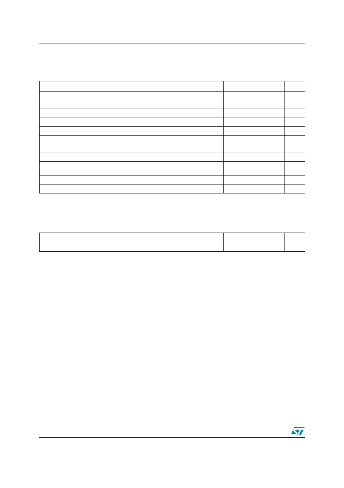
1 Absolute Maximum Ratings
Table 1. Absolute Maximum Ratingsn
Symbol Parameter Value Unit
V
V
V
P
T
CES
CEO
EBO
I
I
CM
I
I
BM
TOT
V
STG
T
Collector-Emitter Voltage (VBE = 0)
Collector-Emitter Voltage (IB = 0)
Emitte-Base Voltage (IC = 0)
Collector Current 26 A
C
Collector Peak Current (tP < 5ms)
Base Current 10 A
B
Base Peak Current (tP < 5ms)
Total dissipation at Tc = 25°C
Insulation Withst and Volt age (RMS ) from All Three Leads to
ins
1500 V
700 V
10 V
40 A
20 A
70 W
2500 V
External Heatsink
Storage Temperature -65 to 150 °C
Max. Operating Junction Temperature 150 °C
J
1.1 Thermal Data
Table 2. Thermal Data
Symbol Parameter Value Unit
R
thJC
Thermal Resistance Junction-Case____________________Max 1.8 °C/W
2/7
Page 3
HD1530FX 2 Electrical Char acteristics
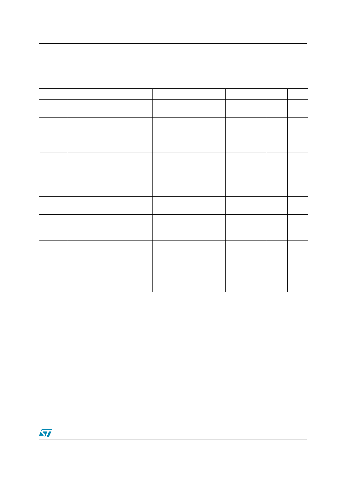
2 Electrical Characteristics
Table 3. Electrical Characteristics (T
= 25°C; unless otherwise specified)
CASE
Symbol Parameter Test Conditions Min. T yp. Max. Unit
V
I
CES
I
EBO
V
CEO(SUS)
Note: 1
V
EBO
V
CE(sat)
Note: 1
V
BE(sat)
Collector Cut-off Current
(V
= 0)
BE
Emitter Cut-off Current
= 0)
(I
C
Collector-Emitter
Sustaining Voltage (I
= 0)
B
Emitter-Base Voltage
Collec tor-Emitter saturatio n
Voltage
Base-Emitter saturation Volt age
= 1500V
CE
V
= 1500V____TC = 125°C
CE
V
= 5V 10 μA
EB
I
= 10mA 700 V
C
I
= 10mA 10 V
E
I
= 13A _____ IB = 3.25A 2 V
C
I
= 13A _____ IB = 3.25A 1 1.5 V
C
0.2
2
Note: 1
h
FE
t
t
t
t
t
t
DC Current Gain IC = 1A _____ V
INDUCTIVE LOAD
Storage Time
s
Fall Time
f
INDUCTIVE LOAD
Storage Time
s
Fall Time
f
INDUCTIVE LOAD
Storage Time
s
Fall Time
f
= 5V
CE
I
= 13A ____ V
C
= 12A ____ _ fh = 32KHz
I
C
I
= 1.4A ___ I
B(on)
= 12A _____ fh = 48KHz
I
C
= 2A ____ I
I
B(on)
= 6.5A _____ fh = 100KHz
I
C
I
= 0.8A ___ I
B(on)
CE
B(off)
B(off)
B(off)
= 5V
= -6.7A
5.5
= -6A
= -4.5A
30
9
3.2
230
2.8
200
1.4
100
mA
mA
μs
ns
μs
ns
μs
ns
Note: 1 Pulsed duration = 300 μs, duty cycle ≤1.5%.
3/7
Page 4

3 Package Mechani cal Data HD1530FX
3 Package M echanical Da ta
In order to meet environmental requirements, ST offers these devices in ECOPACK®
packages. These packages have a Lead-free second level interconnect . The category of
second level interconnect is marked on the package and on the inner box label, in compliance
with JEDEC Standard JESD97. The maximum ratings related to soldering conditions are also
marked on the inner box label. ECOPACK is an ST trademark. ECOPACK specifications are
available at: www.st.com
4/7
Page 5
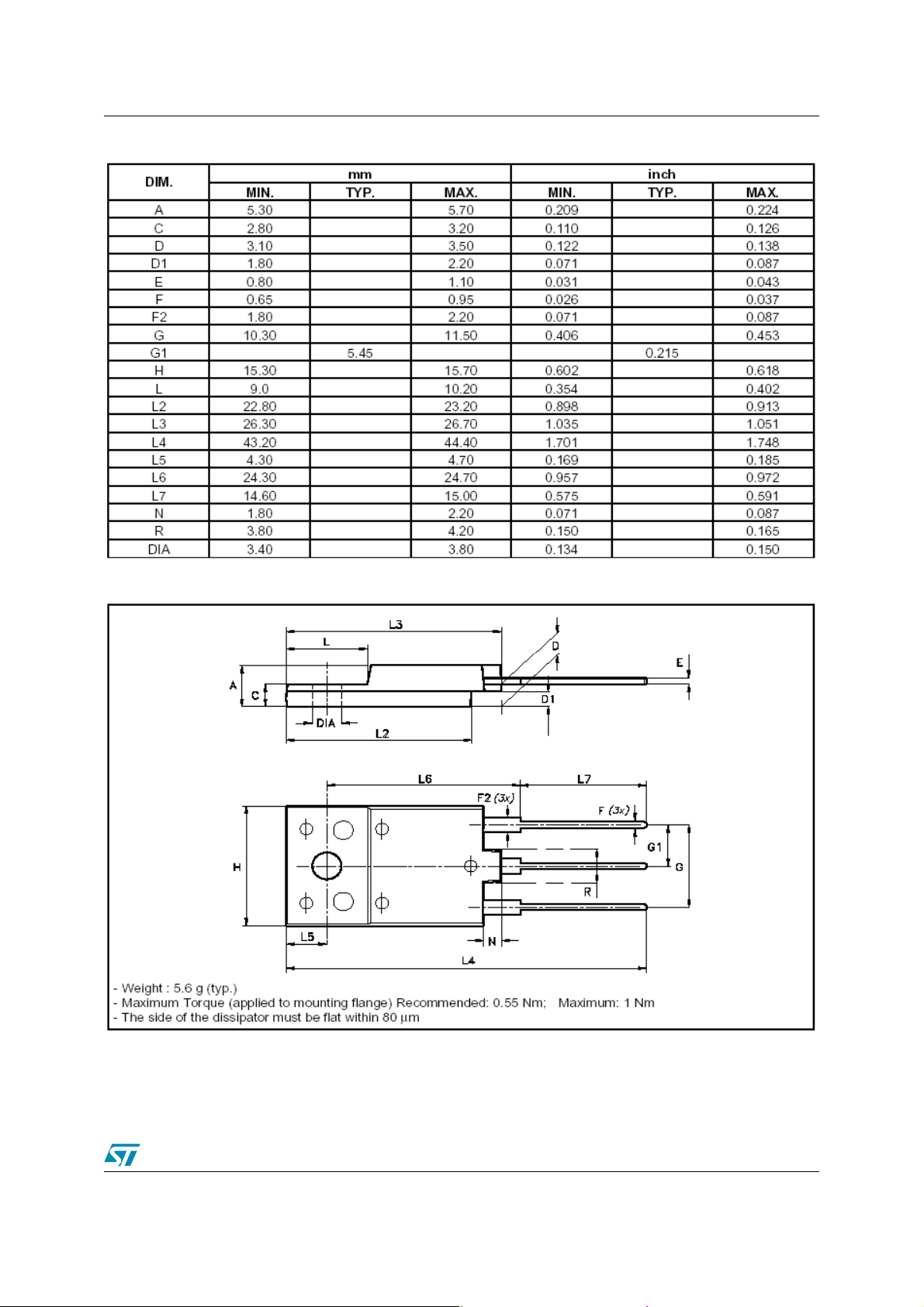
HD1530FX 3 Package Mechanical Data
Table 4. ISOWATT218FX Mechanica l Data
Figure 1. ISOWATT218FX Drawing
5/7
Page 6
4 Revision Hist ory HD1530FX
4 Revision History
Date Revision Changes
05-July-2005 1 Initi al release.
25-July-2005 2 New Template, no content change
19-Aug-2005 3 New ECOPACK® label
6/7
Page 7

HD1530FX 4 Revision History
I
s
o
d
b
ct
t
ot
a
nformation furnished is believed to be accurate and reliable. However, STMicroelectronics assumes no responsibility for the consequence
f use of such information nor for any infringement of patents or other rights of third parties which may result from its use. No license is grante
y implic ation or otherwise under any patent or patent ri ghts of STM i croelectr onics. Specifications menti oned in thi s publicati on are subje
o change without notice. This publication supersedes and replaces all information previously supplied. STMicroelectronics products are n
uthoriz ed for use as critical compo nents in life support devic es or systems without express writt en approval of STMicroel ectronics.
The ST logo is a registered t rademark of S TM i croelectr oni cs.
All other nam es are the pro perty of thei r respectiv e owners
© 2005 STMi croelectronics - All ri ght s reserved
Austra l i a - Be l gi um - Brazil - Canada - Chi na - Czech Rep ubl i c - Finland - F rance - Germ any - Hong Kon g - In di a - Israel - It aly - Japan -
Malaysi a - M al ta - Morocco - Singapore - Spain - Swe den - Switzerland - Un i te d Kingdom - United States of America
STMicroelectron ics group of com panies
www.st.com
7/7
 Loading...