

Page 1
8
7
6
1
3
SHIELD
5
2
4
**V
DD1
V
I
*
GND
1
V
DD2
**
V
O
GND
2
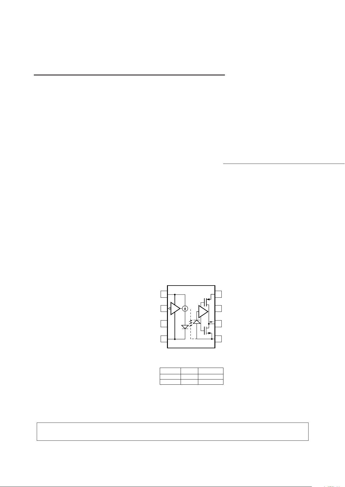
VI, INPUT LED1
H
L
OFF
ON
TRUTH TABLE
(POSITIVE LOGIC)
NC*
I
O
LED1
V
O
, OUTPUT
H
L
H
40 ns Prop. Delay,
SO-8 Optocoupler
Technical Data
HCPL-0710
Functional Diagram
*Pin 3 is the anode of the internal LED and must be left unconnected for guaranteed data sheet performance.
Pin 7 is not connected internally. External connections to pin 7 are not recommended.
**A 0.1 µF bypass capacitor must be connected between pins 1 and 4, and 5 and 8.
CAUTION: It is advised that normal static precautions be taken in handling and assembly of this component
to prevent damage and/or degradation which may be induced by ESD.
Features
• +5 V CMOS Compatibility
• 8 ns max. Pulse Width
Distortion
• 20 ns max. Prop. Delay Skew
• High Speed: 12 Mbd
• 40 ns max. Prop. Delay
• 10 kV/µs Minimum Common
Mode Rejection
• 0°C to 85°C Temp. Range
• Safety and Regulatory
Approvals
UL Recognized
2500 V rms for 1 min. per
UL 1577
CSA Component Acceptance
Notice #5
Applications
• Digital Fieldbus Isolation:
DeviceNet, SDS, Profibus
• AC Plasma Display Panel
Level Shifting
• Multiplexed Data
Transmission
• Computer Peripheral
Interface
• Microprocessor System
Interface
Description
Available in the SO-8 package
style, the HCPL-0710 optocoupler
utilizes the latest CMOS IC
technology to achieve outstanding
performance with very low power
consumption. The HCPL-0710
requires only two bypass
capacitors for complete CMOS
compatability.
Basic building blocks of the
HCPL-0710 are a CMOS LED
driver IC, a high speed LED and a
CMOS detector IC. A CMOS logic
input signal controls the LED
driver IC which supplies current
to the LED. The detector IC
incorporates an integrated
photodiode, a high-speed
transimpedance amplifier, and a
voltage comparator with an
output driver.
Page 2
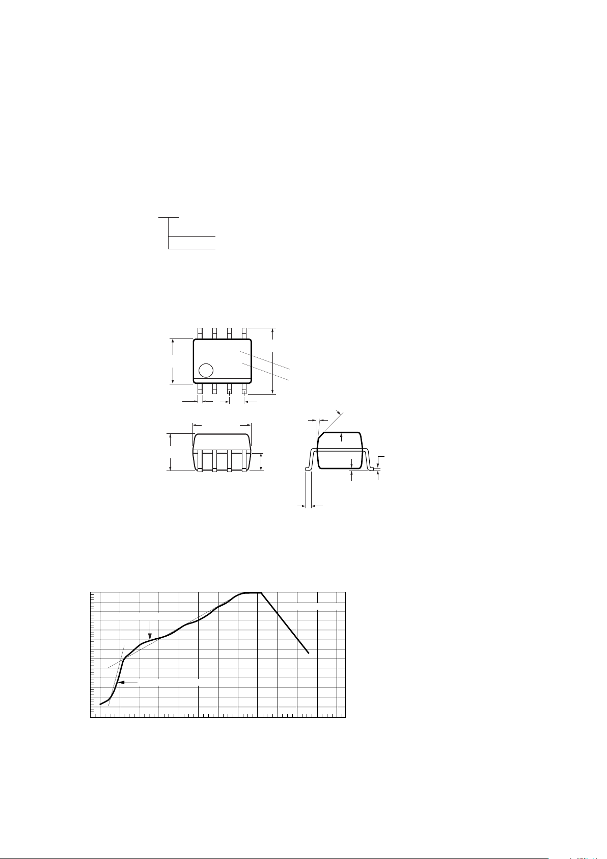
710
YWW
87
65
4
3
2
1
PIN
ONE
7°
5.842 ± 0.203
(0.236 ± 0.008)
3.937 ± 0.127
(0.155 ± 0.005)
0.381 ± 0.076
(0.016 ± 0.003)
1.270
(0.050)
BSG
5.080 ± 0.005
(0.200 ± 0.005)
3.175 ± 0.127
(0.125 ± 0.005)
1.524
(0.060)
45° X
0.432
(0.017)
0.228 ± 0.025
(0.009 ± 0.001)
0.152 ± 0.051
(0.006 ± 0.002)
TYPE NUMBER (LAST 3 DIGITS)
DATE CODE
DIMENSIONS IN MILLIMETERS AND (INCHES).
LEAD COPLANARITY = 0.10 mm (0.004 INCHES).
0.305
(0.012)
MIN.
Ordering Information
Specify Part Number followed by Option Number (if desired)
Example
HCPL-0710#XXX
No Option = Standard SO-8 package, 100 per tube.
500 = Tape and Reel Packaging Option, 1500 per reel.
Option data sheets available. Contact Hewlett-Packard sales representative or authorized distributor.
Package Outline Drawing
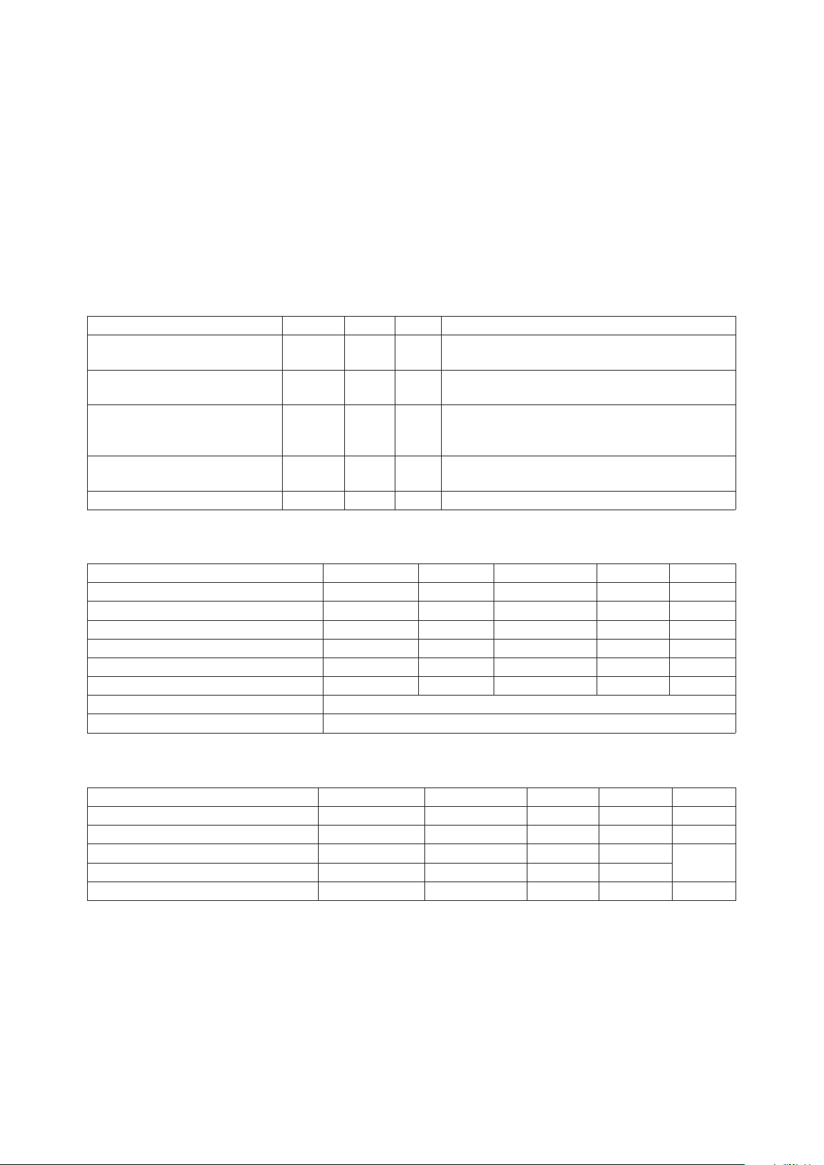
Solder Reflow Thermal Profile
240
∆T = 115°C, 0.3°C/SEC
0
∆T = 100°C, 1.5°C/SEC
∆T = 145°C, 1°C/SEC
TIME – MINUTES
TEMPERATURE – °C
220
200
180
160
140
120
100
80
60
40
20
0
260
123456789101112
(NOTE: USE OF NON-CHLORINE ACTIVATED FLUXES IS RECOMMENDED.)
Page 3
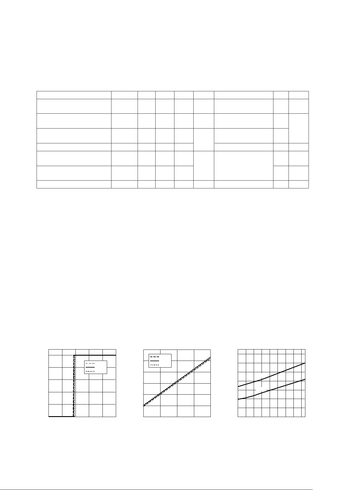
Recommended Operating Conditions
Parameter Symbol Min. Max. Units Figure
Ambient Operating Temperature T
A
0 +85 °C
Supply Voltages V
DD1
, V
DD2
4.5 5.5 V
Logic High Input Voltage V
IH
0.8 * V
DD1
V
DD1
V 1, 2
Logic Low Input Voltage V
IL
0.0 0.8 V
Input Signal Rise and Fall Times tr, t
f
1.0 ms
Regulatory Information
The HCPL-0710 has been
approved by the following
organizations:
UL
Recognized under UL 1577,
component recognition program,
File E55361.
Absolute Maximum Ratings
Parameter Symbol Min. Max. Units Figure
Storage Temperature T
S
-55 125 °C
Ambient Operating Temperature
[1]
T
A
-40 +100 °C
Supply Voltages V
DD1
, V
DD2
0 5.5 Volts
Input Voltage V
I
-0.5 V
DD1
+0.5 Volts
Output Voltage V
O
-0.5 V
DD2
+0.5 Volts
Average Output Current I
O
10 mA
Lead Solder Temperature 260°C for 10 sec., 1.6 mm below seating plane
Solder Reflow Temperature Profile See Solder Reflow Temperature Profile Section
Insulation and Safety Related Specifications
Parameter Symbol Value Units Conditions
Minimum External Air Gap L(I01) 4.9 mm Measured from input terminals to output
(Clearance) terminals, shortest distance through air.
Minimum External Tracking L(I02) 4.8 mm Measured from input terminals to output
(Creepage) terminals, shortest distance path along body.
Minimum Internal Plastic Gap 0.08 mm Insulation thickness between emitter and
(Internal Clearance) detector; also known as distance through
insulation.
Tracking Resistance CTI 200 Volts DIN IEC 112/VDE 0303 Part 1
(Comparative Tracking Index)
Isolation Group IIIa Material Group (DIN VDE 0110, 1/89, Table 1)
CSA
Approved under CSA Component
Acceptance Notice #5, File CA
88324.
Page 4
Electrical Specifications
Test conditions that are not specified can be anywhere within the recommended operating range. All typical
specifications are at TA = +25°C, V
DD1
= V
DD2
= +5 V.
Parameter Symbol Min. Typ. Max. Units Test Conditions Fig. Note
DC Specifications
Logic Low Input I
DD1L
6.0 10.0 mA VI = 0 V 2
Supply Current
Logic High Input I
DD1H
1.5 3.0 mA VI = V
DDI
Supply Current
Input Supply Current I
DD1
13.0 mA
Output Supply Current I
DD2
5.5 11.0 mA
Input Current I
I
-10 10 µA
Logic High Output V
OH
V
DD2
- 0.1 V
DD2
VIO = -20 µA, VI = VIH1, 2
0.8 *V
DD2VDD2
- 0.5 IO = -4 mA, VI = V
IH
Logic Low Output V
OL
0 0.1 V IO = 20 µA, VI = V
IL
0.5 1.0 IO = 4 mA, VI = V
IL
Switching
Propagation Delay Time t
PHL
20 40 ns CL = 15 pF 3, 7 3
to Logic Low Output CMOS Signal Levels
Propagation Delay Time t
PLH
23 40
to Logic High Output
Pulse Width PW 80 4
Data Rate 12.5 MBd
Pulse Width Distortion PWD 3 8 ns CL = 15 pF 4, 8 5
|t
PHL
- t
PLH
| CMOS Signal Levels
Propagation Delay Skew t
PSK
20 6
Output Rise Time t
R
9C
L
= 15 pF 5, 9
(10 - 90%) CMOS Signal Levels
Output Fall Time t
F
86,
(90 - 10%) 10
Common Mode |CMH| 10 20 kV/µsVI = V
DD1
, VO >7
Transient Immunity at 0.8 V
DD1
,
Logic High Output VCM = 1000 V
Common Mode |CML|10 20 V
I
= 0 V, VO > 0.8 V,
Transient Immunity at VCM = 1000 V
Logic Low Output
Input Dynamic Power C
PD1
60 pF 8
Dissipation
Capacitance
Output Dynamic Power C
PD2
10
Dissipation
Capacitance
Voltage
Voltage
Specifications
Page 5
Package Characteristics
Parameter Symbol Min. Typ. Max. Units Test Conditions Fig. Note
Input-Output Momentary V
ISO
2500 Vrms RH ≤ 50%, t = 1 min., 9, 10,
Withstand Voltage TA = 25°C11
Resistance R
I-O
10
12
Ω V
I-O
= 500 Vdc 9
(Input-Output)
Capacitance C
I-O
0.6 pF f = 1 MHz
(Input-Output)
Input Capacitance C
I
3.0 12
Input IC Junction-to-Case θ
jci
160 °C/W Thermocouple
Thermal Resistance located at center
Output IC Junction-to-Case θ
jco
135
Thermal Resistance
Package Power Dissipation P
PD
150 mW
Notes:
1. Absolute Maximum ambient operating
temperature means the device will not
be damaged if operated under these
conditions. It does not guarantee
functionality.
2. The LED is ON when VI is low and OFF
when VI is high.
3. t
PHL
propagation delay is measured
from the 50% level on the falling edge
of the VI signal to the 50% level of the
falling edge of the VO signal. t
PLH
propagation delay is measured from
the 50% level on the rising edge of the
VI signal to the 50% level of the rising
edge of the VO signal.
4. Mimimum Pulse Width is the shortest
pulse width at which 10% maximum,
Pulse Width Distortion can be guaranteed. Maximum Data Rate is the
inverse of Minimum Pulse Width.
Operating the HCPL-0710 at data rates
above 12.5 MBd is possible provided
PWD and data dependent jitter
increases and relaxed noise margins
underside of
package
are tolerable within the application.
For instance, if the maximum
allowable variation of bit width is 30%,
the maximum data rate becomes 37.5
MBd. Please note that HCPL-0710
performance above 12.5 MBd is not
guaranteed by Hewlett-Packard.
5. PWD is defined as |t
PHL
- t
PLH
|.
%PWD (percent pulse width distortion)
is equal to the PWD divided by pulse
width.
6. t
PSK
is equal to the magnitude of the
worst case difference in t
PHL
and/or
t
PLH
that will be seen between units at
any given temperature within the
recommended operating conditions.
7. CMH is the maximum common mode
voltage slew rate that can be sustained
while maintaining VO > 0.8 V
DD2
. CM
L
is the maximum common mode voltage
slew rate that can be sustained while
maintaining VO < 0.8 V. The common
mode voltage slew rates apply to both
rising and falling common mode
voltage edges.
8. Unloaded dynamic power dissipation is
calculated as follows: CPD * V
DD2
* f +
IDD * VDD, where f is switching
frequency in MHz.
9. Device considered a two-terminal
device: pins 1, 2, 3, and 4 shorted
together and pins 5, 6, 7, and 8
shorted together.
10. In accordance with UL1577, each
optocoupler is proof tested by
applying an insulation test voltage
≥ 3000 V
RMS
for 1 second (leakage
detection current limit, I
I-O
≤ 5 µA).
11. The Input-Output Momentary Withstand Voltage is a dielectric voltage
rating that should not be interpreted as
an input-output continuous voltage
rating. For the continuous voltage
rating refer to your equipment level
safety specification or HP Application
Note 1074 entitled “Optocoupler
Input-Output Endurance Voltage.”
12. CI is the capacitance measured at pin
2 (VI).
Figure 1. Typical Output Voltage vs.
Input Voltage.
Figure 2. Typical Input Voltage
Switching Threshold vs. Input Supply
Voltage.
Figure 3. Typical Propagation Delays
vs. Temperature.
V
O
(V)
0
0
VI (V)
5
4
1
4123
5
3
2
0 °C
25 °C
85 °C
V
ITH
(V)
4.5
1.6
V
DD1
(V)
5.5
2.1
1.7
5.254.75 5
2.2
2.0
1.8
1.9
0 °C
25 °C
85 °C
T
PLH
, T
PHL
(ns)
0
15
TA (C)
80
27
17
6020 30
29
25
19
21
10 40 50 70
23
T
PLH
T
PHL
Page 6

Figure 10. Typical Fall Time vs. Load
Capacitance.
Figure 4. Typical Pulse Width
Distortion vs. Temperature.
Figure 5. Typical Rise Time vs.
Temperature.
Figure 6. Typical Fall Time vs.
Temperature.
Figure 7. Typical Propagation Delays
vs. Output Load Capacitance.
Figure 8. Typical Pulse Width
Distortion vs. Output Load
Capacitance.
Figure 9. Typical Rise Time vs. Load
Capacitance.
PWD
(ns)
0
0
TA (C)
80
3
6020
4
1
40
2
T
R
(ns)
0
12
TA (C)
80
14
6020
15
13
40
T
F
(ns)
0
2
TA (C)
80
6
6020
7
3
40
5
4
T
PLH
, T
PHL
(ns)
0
15
CI (pF)
35
27
25
29
17
15
23
21
1052030
19
25
T
PLH
T
PHL
PWD
(ns)
0
0
CI (pF)
35
5
25
6
1
15
3
1052030
2
4
T
R
(ns)
0
5
CI (pF)
35
23
25
25
9
15
15
1052030
11
19
21
17
13
7
FALL TIME
(ns)
0
0
CI (pF)
35
9
25
10
2
15
5
1052030
3
7
8
6
4
1
Page 7

Application Information
Bypassing and PC Board
Layout
The HCPL-0710 optocoupler is
extremely easy to use. No
external interface circuitry is
required because the HCPL-0710
uses high-speed CMOS IC
technology allowing CMOS logic
to be connected directly to the
inputs and outputs.
As shown in Figure 11, the only
external components required for
proper operation are two bypass
capacitors. Capacitor values
should be between 0.01 µF and
0.1 µF. For each capacitor, the
total lead length between both
ends of the capacitor and the
power-supply pins should not
exceed 20 mm. Figure 12
illustrates the recommended
printed circuit board layout for
the HPCL-0710.
Figure 11. Recommended Printed Circuit Board Layout.
Figure 12. Recommended Printed Circuit Board Layout.
7
5
6
8
2
3
4
1
GND
2
C1 C2
NC
V
DD2
NC
V
O
V
DD1
V
I
710
YYWW
C1, C2 = 0.01 µF TO 0.1 µF
GND
1
V
DD2
C1 C2
710
YYWW
V
O
GND
2
V
DD1
V
I
GND
1
C1, C2 = 0.01 µF TO 0.1 µF
Page 8

Propagation Delay, PulseWidth Distortion and
Propagation Delay Skew
Propagation Delay is a figure of
merit which describes how
quickly a logic signal propagates
through a system. The propaga-
tion delay from low to high (t
PLH
)
is the amount of time required for
an input signal to propagate to
the output, causing the output to
change from low to high.
Similarly, the propagation delay
from high to low (t
PHL
) is the
amount of time required for the
input signal to propagate to the
output, causing the output to
change from high to low. See
Figure 13.
Figure 13.
Pulse-width distortion (PWD) is
the difference between t
PHL
and
t
PLH
and often determines the
maximum data rate capability of a
transmission system. PWD can be
expressed in percent by dividing
the PWD (in ns) by the minimum
pulse width (in ns) being transmitted. Typically, PWD on the
order of 20 - 30% of the minimum
pulse width is tolerable. The PWD
specification for the HCPL-0710
is 8 ns (10%) maximum across
recommended operating conditions. 10% maximum is dictated
by the most stringent of the three
fieldbus standards, PROFIBUS.
Propagation delay skew, t
PSK
, is
an important parameter to consider in parallel data applications
where synchronization of signals
on parallel data lines is a concern.
If the parallel data is being sent
through a group of optocouplers,
differences in propagation delays
will cause the data to arrive at the
outputs of the optocouplers at
different times. If this difference
in propagation delay is large
enough it will determine the
maximum rate at which parallel
data can be sent through the
optocouplers.
Propagation delay skew is defined
as the difference between the
minimum and maximum propagation delays, either t
PLH
or t
PHL
,
for any given group of optocouplers which are operating under
the same conditions (i.e., the
same drive current, supply voltage, output load, and operating
temperature). As illustrated in
Figure 14, if the inputs of a group
of optocouplers are switched
either ON or OFF at the same
time, t
PSK
is the difference
between the shortest propagation
delay, either t
PLH
or t
PHL
, and the
longest propagation delay, either
t
PLH
or t
PHL
.
As mentioned earlier, t
PSK
can
determine the maximum parallel
data transmission rate. Figure 15
is the timing diagram of a typical
parallel data application with both
the clock and data lines being
sent through the optocouplers.
The figure shows data and clock
signals at the inputs and outputs
of the optocouplers. In this case
the data is assumed to be clocked
off of the rising edge of the clock.
INPUT
t
PLH
t
PHL
OUTPUT
V
I
V
O
10%
90%90%
10%
V
OH
V
OL
0 V
50%
5 V CMOS
2.5 V CMOS
Page 9

Figure 14. Propagation Delay Skew Waveform. Figure 15. Parallel Data Transmission Example.
Propagation delay skew represents the uncertainty of where an
edge might be after being sent
through an optocoupler.
Figure 15 shows that there will be
uncertainty in both the data and
clock lines. It is important that
these two areas of uncertainty not
overlap, otherwise the clock
signal might arrive before all of
the data outputs have settled, or
some of the data outputs may
start to change before the clock
signal has arrived. From these
considerations, the absolute
minimum pulse width that can be
sent through optocouplers in a
parallel application is twice t
PSK
.
A cautious design should use a
slightly longer pulse width to
ensure that any additional
uncertainty in the rest of the
circuit does not cause a problem.
The HCPL-0710 optocoupler
offers the advantage of
guaranteed specifications for
propagation delays, pulse-width
distortion, and propagation delay
skew over the recommended
temperature and power supply
ranges.
50%
50%
t
PSK
V
I
V
O
V
I
V
O
2.5 V,
CMOS
2.5 V,
CMOS
DATA
INPUTS
CLOCK
DATA
OUTPUTS
CLOCK
t
PSK
t
PSK
Page 10

Optical Isolation for
Field Bus Networks
To recognize the full benefits of
these networks, each recommends providing galvanic
isolation using Hewlett-Packard
optocouplers. Since network
communication is bi-directional
(involving receiving data from
and transmitting data onto the
network), two Hewlett-Packard
optocouplers are needed. By
providing galvanic isolation, data
integrity is retained via noise
reduction and the elimination of
Figure 16. Typical Field Bus Communication Physical Model.
false signals. In addition, the
network receives maximum
protection from power system
faults and ground loops.
Within an isolated node, such as
the DeviceNet Node shown in
Figure 17, some of the node’s
components are referenced to a
ground other than V- of the
network. These components could
include such things as devices
with serial ports, parallel ports,
RS232 and RS485 type ports. As
shown in Figure 17, power from
the network is used only for the
transceiver and input (network)
side of the optocouplers.
Isolation of nodes connected to
any of the three types of digital
field bus networks is best
achieved by using the HCPL-0710
optocoupler. For each network,
the HCPL-0710 satisifies the
critical propagation delay and
pulse width distortion requirements over the temperature range
of 0°C to +85°C, and power
supply voltage range of 4.5 V
to 5.5 V.
Digital Field Bus
Communication
Networks
To date, despite its many drawbacks, the 4 - 20 mA analog
current loop has been the most
widely accepted standard for
implementing process control
systems. In today’s manufacturing
environment, however, automated
systems are expected to help
manage the process, not merely
monitor it. With the advent of
digital field bus communication
networks such as DeviceNet,
PROFIBUS, and Smart Distributed
Systems (SDS), gone are the days
of constrained information.
Controllers can now receive
multiple readings from field
devices (sensors, actuators, etc.)
in addition to diagnostic
information.
The physical model for each of
these digital field bus communication networks is very similar as
shown in Figure 16. Each
includes one or more buses, an
interface unit, optical isolation,
transceiver, and sensing and/or
actuating devices.
CONTROLLER
TRANSCEIVER
OPTICAL
ISOLATION
BUS
INTERFACE
TRANSCEIVER
OPTICAL
ISOLATION
BUS
INTERFACE
TRANSCEIVER
OPTICAL
ISOLATION
BUS
INTERFACE
TRANSCEIVER
OPTICAL
ISOLATION
BUS
INTERFACE
TRANSCEIVER
OPTICAL
ISOLATION
BUS
INTERFACE
FIELD BUS
XXXXXX
YYY
SENSOR
DEVICE
CONFIGURATION
MOTOR
STARTER
MOTOR
CONTROLLER
Page 11

Implementing DeviceNet
and SDS with the
HCPL-0710
With transmission rates up to 1
Mbit/s, both DeviceNet and SDS
are based upon the same
broadcast-oriented, communications protocol — the Controller
Area Network (CAN). Three types
of isolated nodes are
recommended for use on these
networks: Isolated Node Powered
Figure 17. Typical DeviceNet Node.
by the Network (Figure 18),
Isolated Node with Transceiver
Powered by the Network (Figure
19), and Isolated Node Providing
Power to the Network
(Figure 20).
Isolated Node Powered by the
Network
This type of node is very flexible
and as can be seen in Figure 18,
is regarded as “isolated” because
not all of its components have the
Figure 18. Isolated Node Powered by the Network.
same ground reference. Yet, all
components are still powered by
the network. This node contains
two regulators: one is isolated and
powers the CAN controller, nodespecific application and isolated
(node) side of the two optocouplers while the other is nonisolated. The non-isolated
regulator supplies the transceiver
and the non-isolated (network)
half of the two optocouplers.
NODE/APP SPECIFIC
uP/CAN
HCPL
0710
HCPL
0710
TRANSCEIVER
LOCAL
NODE
SUPPLY
5 V REG.
NETWORK
POWER
SUPPLY
V+ (SIGNAL)
V– (SIGNAL)
V+ (POWER)
V– (POWER)
GALVANIC
ISOLATION
BOUNDARY
AC LINE
DRAIN/SHIELD
SIGNAL
POWER
NODE/APP SPECIFIC
uP/CAN
HCPL
0710
HCPL
0710
TRANSCEIVER
REG.
V+ (SIGNAL)
V– (SIGNAL)
V+ (POWER)
V– (POWER)
GALVANIC
ISOLATION
BOUNDARY
DRAIN/SHIELD
SIGNAL
POWER
ISOLATED
SWITCHING
POWER
SUPPLY
NETWORK
POWER
SUPPLY
Page 12

Figure 19. Isolated Node with Transceiver Powered by the Network.
Isolated Node with
Transceiver Powered by the
Network
Figure 19 shows a node powered
by both the network and another
source. In this case, the transceiver and isolated (network) side
of the two optocouplers are
powered by the network. The rest
of the node is powered by the AC
line which is very beneficial when
an application requires a
significant amount of power. This
method is also desirable as it does
not heavily load the network.
NODE/APP SPECIFIC
uP/CAN
HCPL
0710
HCPL
0710
TRANSCEIVER
NON ISO
5 V
REG.
NETWORK
POWER
SUPPLY
V+ (SIGNAL)
V– (SIGNAL)
V+ (POWER)
V– (POWER)
GALVANIC
ISOLATION
BOUNDARY
AC LINE
DRAIN/SHIELD
SIGNAL
POWER
More importantly, the unique
“dual-inverting” design of the
HCPL-0710 ensures the network
will not “lock-up” if either AC line
power to the node is lost or the
node powered-off. Specifically,
when input power (V
DD1
) to the
HCPL-0710 located in the
transmit path is eliminated, a
RECESSIVE bus state is ensured
as the HCPL-0710 output voltage
(VO) goes HIGH.
Page 13

Figure 20. Isolated Node Providing Power to the Network.
Isolated Node Providing
Power to the Network
Figure 20 shows a node providing
power to the network. The AC line
powers a regulator which
provides five (5) volts locally. The
AC line also powers a 24 volt
isolated supply, which powers the
network, and another five-volt
regulator, which, in turn, powers
the transceiver and isolated
(network) side of the two
optocouplers. This method is
recommended when there are a
limited number of devices on the
network that don’t require much
power, thus eliminating the need
for separate power supplies.
NODE/APP SPECIFIC
uP/CAN
HCPL
0710
HCPL
0710
TRANSCEIVER
5 V REG.
V+ (SIGNAL)
V– (SIGNAL)
V+ (POWER)
V– (POWER)
GALVANIC
ISOLATION
BOUNDARY
AC LINE
DRAIN/SHIELD
SIGNAL
POWER
ISOLATED
SWITCHING
POWER
SUPPLY
5 V REG.
DEVICENET NODE
More importantly, the unique
“dual-inverting” design of the
HCPL-0710 ensures the network
will not “lock-up” if either AC line
power to the node is lost or the
node powered-off. Specifically,
when input power (V
DD1
) to the
HCPL-0710 located in the
transmit path is eliminated, a
RECESSIVE bus state is ensured
as the HCPL-0710 output voltage
(VO) goes HIGH.
Page 14

8
7
6
1
3
5
2
4
V
DD1
V
IN
GND
1
V
DD2
V
O
GND
2
HCPL-0710
4
3
2
5
7
1
6
8
GND
2
V
O
V
DD2
GND
1
V
IN
V
DD1
HCPL-0710
GND
ISO 5 V
ISO 5 V
0.01 µF
RX0
0.01 µF
TX0
0.01
µF
0.01
µF
TxD
CANH
REF
RXD
82C250
V
CC
GND
Rs
CANL
C4
0.01 µF
+
VREF
LINEAR OR
SWITCHING
REGULATOR
5 V
5 V
++
R1
1 M
C1
0.01 µF
500 V
D1
30 V
5 V+
4 CAN+
3 SHIELD
2 CAN–
1 V–
GALVANIC
ISOLATION
BOUNDARY
Power Supplies and Bypassing
The recommended DeviceNet
application circuit is shown in
Figure 21. Since the HCPL-0710
is fully compatible with CMOS
logic level signals, the optocoupler is connected directly to the
Figure 21. Recommended DeviceNet Application Circuit.
Implementing PROFIBUS
with the HCPL-0710
An acronym for Process Fieldbus,
PROFIBUS is essentially a
twisted-pair serial link very
similar to RS-485 capable of
achieving high-speed communication up to 12 MBd. As shown in
Figure 22, a PROFIBUS Controller (PBC) establishes the connec-
CAN transceiver. Two bypass
capacitors (with values between
0.01 and 0.1 µF) are required and
should be located as close as
possible to the input and output
power-supply pins of the HCPL-
0710. For each capacitor, the
tion of a field automation unit
(control or central processing
station) or a field device to the
transmission medium. The PBC
consists of the line transceiver,
optical isolation, frame character
transmitter/receiver (UART), and
the FDL/APP processor with the
interface to the PROFIBUS user.
Figure 22. PROFIBUS Controller
(PBC).
PROFIBUS USER:
CONTROL STATION
(CENTRAL PROCESSING)
OR FIELD DEVICE
USER INTERFACE
FDL/APP
PROCESSOR
TRANSCEIVER
OPTICAL ISOLATION
UART
PBC
MEDIUM
total lead length between both
ends of the capacitor and the
power supply pins should not
exceed 20 mm. The bypass capacitors are required because of the
high-speed digital nature of the
signals inside the optocoupler.
Page 15

Figure 23. Recommended PROFIBUS Application Circuit.
Power Supplies and
Bypassing
The recommended PROFIBUS
application circuit is shown in
Figure 23. Since the HCPL-0710
is fully compatible with CMOS
logic level signals, the
optocoupler is connected directly
to the transceiver. Two bypass
capacitors (with values between
0.01 and 0.1 µF) are required and
should be located as close as
possible to the input and output
power-supply pins of the HCPL-
0710. For each capacitor, the
total lead length between both
ends of the capacitor and the
power supply pins should not
exceed 20 mm. The bypass
capacitors are required because
of the high-speed digital nature of
the signals inside the optocoupler.
Being very similar to multi-station
RS485 systems, the HCPL-061N
optocoupler provides a transmit
disable function which is neces-
sary to make the bus free after
each master/slave transmission
cycle. Specifically, the HCPL061N disables the transmitter of
the line driver by putting it into a
high state mode. In addition, the
HCPL-061N switches the RX/TX
driver IC into the listen mode. The
HCPL-061N offers HCMOS
compatibility and the high CMR
performance (1 kV/µs at VCM =
1000 V) essential in industrial
communication interfaces.
1
2
3
8
6
4
7
5
V
DD2
V
O
GND
2
V
DD1
V
IN
GND
1
HCPL-0710
8
7
6
1
3
5
2
4
V
DD1
V
IN
GND
1
V
DD2
V
O
GND
2
HCPL-0710
ISO 5 V
0.01 µF
0.01 µF
0.01
µF
0.01
µF
R
A
SN75176B
V
CC
GND
RE
B
0.01
µF
5 V
1 M
0.01 µF
+
–
GALVANIC
ISOLATION
BOUNDARY
ISO 5 V 5 V
DE
D
1
4
2
3
Rx
5 V
Tx
8
7
6
1
3
5
2
4
ANODE
V
CC
V
O
GND
ISO 5 V
0.01
µF
5 V
Tx ENABLE
CATHODE
V
E
1 kΩ
HCPL-061N
1, 5 kΩ
5
7
6
8
RT
Page 16

H
For technical assistance or the location of
your nearest Hewlett-Packard sales office,
distributor or representative call:
Americas/Canada: 1-800-235-0312 or
408-654-8675
Far East/Australasia: Call your local HP
sales office.
Japan: (81 3) 3335-8152
Europe: Call your local HP sales office.
Data subject to change.
Copyright © 1997 Hewlett-Packard Co.
Printed in U.S.A. 5965-6033E (1/97)
 Loading...