

Page 1
PRELIMINARY DATA SHEET
MICRONAS
HAL805
Programmable Linear
Hall Effect Sensor
Edition Feb. 2, 2000
6251-513-1PD
MICRONAS
Page 2

HAL805 PRELIMINARY DATA SHEET
Contents
Page Section Title
3 1. Introduction
3 1.1. Major Applications
3 1.2. Features
4 1.3. Marking Code
4 1.4. Operating Junction Temperature Range (T
4 1.5. Hall Sensor Package Codes
4 1.6. Solderability
4 1.7. Pin Connections and Short Descriptions
5 2. Functional Description
5 2.1. General Function
7 2.2. Digital Signal Processing and EEPROM
9 2.3. Calibration Procedure
9 2.3.1. General Procedure
10 2.3.2. Calibration of the Angle Sensor
)
J
11 3. Specifications
11 3.1. Outline Dimensions
11 3.2. Dimensions of Sensitive Area
11 3.3. Position of Sensitive Area
12 3.4. Absolute Maximum Ratings
12 3.5. Recommended Operating Conditions
13 3.6. Electrical Characteristics
14 3.7. Magnetic Characteristics
14 3.8. Open Circuit Detection
15 3.9. Typical Characteristics
17 4. Application Notes
17 4.1. Application Circuit
17 4.2. Use of two HAL 805 in Parallel
17 4.3. Temperature Compensation
18 4.4. Undervoltage Behavior
18 4.5. Am bi ent Te mpe ratur e
18 4.6. EMC and ESD
19 5. Programming of the Sensor
19 5.1. Definition of Programming Pulses
19 5.2. Definition of the Telegram
21 5.3. Telegram Codes
22 5.4. Number Formats
23 5.5. Register Information
23 5.6. Programming Information
24 6. Data Sheet History
Note: Some exclusivity restrictions may apply for the use of this sensor in automotive applications.
2 Micronas
Page 3

PRELIMINARY DATA SHEET HAL805
Programmable Linear Hall Effect Sensor
1. Introduction
The HAL 805 is a recent member of the Micronas family of programmable linear Hall sensors. As an extension to the HAL 800, it offers open-circuit detection and
individual programmi ng of different sensors which are
in parallel to the same supply voltage.
The HAL 805 is an universal magnetic field sensor
with a linear output bas ed on the Hall effect. The IC i s
designed and produ ced in sub-mic ron CMOS techn ology and can be used for angle or distance measurements if combined wit h a rotating or moving magnet.
The major characteristics like magnetic field range,
sensitivity, output quiescent voltage (output voltage at
B = 0 mT), and output voltage range are p rogrammable in a non-volatile memo ry. The sensor has a ratiometric output ch aracter isti c, which mean s th at the output voltage is propor ti on al to the m agn eti c flux and t he
supply voltage.
The HAL 805 features a temperature-compensated
Hall plate with choppered offset compensation, an A/D
converter, digital signal processing, a D/A converter
with output driver, an EEPROM memory with redundancy and lock function for the calibration data, a
serial interface for programming the EEPROM, and
protection devices at all pins. The internal digital signal
processing is of great b enefit because ana log offsets,
temperature shifts, and mechanical stress do not
degrade the sensor accuracy.
The sensor is des igned for hostile ind ustrial a nd automotive applications and operates with typically 5 V
supply voltage in the amb ient temperature range fr om
−40 °C up to 150 °C. The HAL 805 is available in the
very small leaded package TO-92UT.
1.1. Major Applications
Due to the sensor’s versatile programming c haracteristics, the HAL 805 is the optimal s ystem solution for
applications such as:
– contactless potentiometers,
– angle sensors,
– distance measurements,
– magnetic field and current measurement.
1.2. Features
– high-precision linear Hall effect sensor with
ratiometric output and digital signal processing
– multiple programmable magnetic characteristics in a
non-volatile memory (EEPROM) with redundancy
and lock function
– open-circuit detectio n (gro und and su ppl y li ne brea k
detection)
– for programming an individual sensor withi n several
sensors in parallel to the same supply voltage, a
selection can be done via the output pin
The HAL 805 is programmable by modulating the s upply voltage. No additional programming pi n is needed.
The easy programmab ility allows a 2-point calib ration
by adjusting the output voltage directly to the input signal (like mechanic al angle, distance, or curren t). Individual adjustment of each sensor during the customer’s manufacturing process is possible. With this
calibration procedure, the tolerances of the sensor, the
magnet, and the mechanical positioning can be compensated in the final ass embly. This offers a low-cost
alternative for all applications that presently need
mechanical adjustment or laser trimming for calibrating
the system.
In addition, the t emperature compensation of the Hall
IC can be fit to all commo n magne tic mat er ials by programming first and second order temperature coefficients of the Hall sensor sensitivity. This enables operation over the full temperature range with high
accuracy.
The calculation of the indiv idual se nsor cha racteristi cs
and the programming of the EEPROM memory can
easily be done with a PC and the applic ation kit from
Micronas.
– to enable programming of an individual sensor
amongst several sensors running parallel to the
same supply voltage, each sensor can be sel ected
via its output pin
– temperature characteristics are programmable for
matching all common magnetic materials
– programmable clamping function
– programming through a modulation of the supply
voltage
– operates from
ambient temperature
– operates from 4.5 V up to 5.5 V supply voltage in
specification and functions up to 8.5 V
– total error < 2.0% over operating voltage range and
temperature range
– operates with static magnetic fields and dynamic
magnetic fields up to 2 kHz
– overvoltage and reverse-voltage protection at all pins
– magnetic characteristics extremely robust against
mechanical stress
– short-circuit protected push-pull output
−40 °C up to 150 °C
– EMC and ESD optimized design
Micronas 3
Page 4
HAL805 PRELIMINARY DATA SHEET
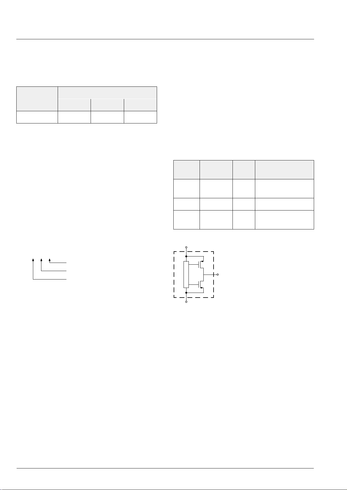
HALXXXPA-T
Temperature Range: A, K, or E
Package: UT for TO-92UT
Type: 805
1.3. Marki n g C o de
The HAL 805 has a marking on the package surface
(branded side). T his m ark ing in clud es the name o f th e
sensor and the temperature range.
Type Temperature Range
A K E
HAL 805 805A 805K 805E
1.4. Operating Junction Temperature Range (T
)
J
The Hall sensors from Micronas are specified to the
chip temperature (junction temperature T
A: TJ =
K: TJ =
E: TJ =
−40 °C to +170 °C
−40 °C to +140 °C
−40 °C to +100 °C
The relationship between ambient temperature (T
).
J
A
and junction temperature is explained in Section 4.5.
on page 18.
1.6. Solderability
Package TO-92UT: according to IEC68-2-58
During soldering reflow processing and manual
reworking, a component body temperature of 260 °C
should not be exceeded.
Components stored in the original packaging should
provide a shelf life of at least 12 m onths, starting fro m
the date code pr inted on the package labels, even in
environments as extreme as 40 °C and 90% relative
humidity.
1.7. Pin Connections and Short Descriptions
Pin
Pin Name Type Short Description
No.
1V
DD
IN Supply Voltage and
Programming Pin
)
2 GND Ground
3 OUT OUT Push Pull Output
and Selection Pin
1.5. Hall Sensor Package Codes
Example: HAL805UT-K
→ Type: 805
→ Package: TO-92UT
→ Temperature Range: T
= −40°C to +140°C
J
Hall sensors are available in a wide variety of packaging versions and quantities. For more detailed information, please refer to the brochure: “Ordering Co des for
Hall Sensors”.
1
V
DD
OUT
3
GND
2
Fig. 1–1: Pin configuration
4 Micronas
Page 5
PRELIMINARY DATA SHEET HAL805
2. Functional Description
2.1. General Function
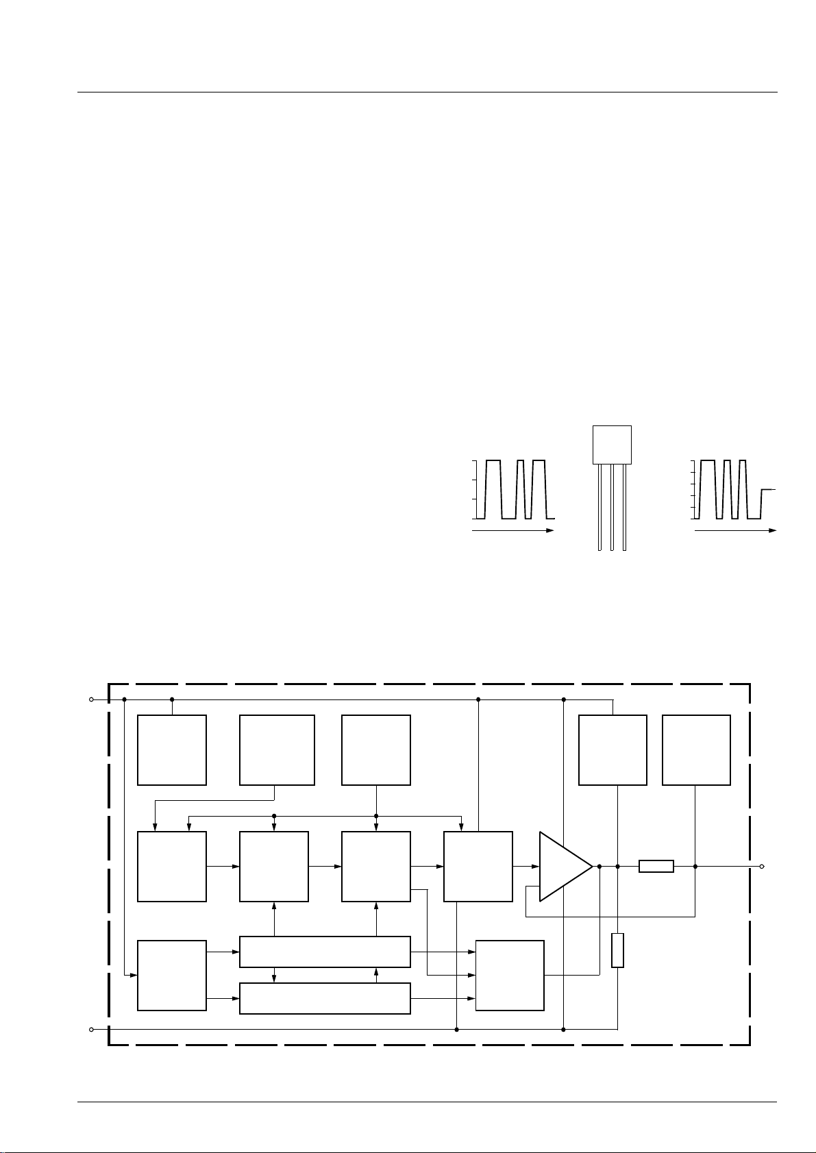
The HAL 805 is a monolithic integrated circuit which
provides an output voltage proportional to the magnetic flux through the Hall pla te an d pr oportional to the
supply voltage (ratiometric behavior).
The external magnetic field component perpendi cular
to the branded side of th e package generates a Hall
voltage. The Hall IC is sensitive to magnetic north and
south polarity. This voltage is converted to a digital
value, processed in the Digital S ignal Processing Unit
(DSP) according to the se tti ngs o f th e E EPROM r egi sters, converted to an analog voltage with ratiometric
behavior, and stabilized by a push-pull output transistor stage. The function and the parameters for the DSP
are explained in Section 2.2. on page 7.
The setting of the LOCK register disables the programming of the EE PROM memor y for all time. This r egister cannot be reset.
As long as the LOCK register is not set, the output
characteristic can be adjusted by programming the
EEPROM registers. The IC is addressed by modulating the supply voltage (see Fig. 2–1). In the supply
voltage range from 4.5 V up to 5.5 V , the sensor generates an analog o utput voltage. After detecting a c ommand, the sensor reads or writes the memory and
answers with a digital signal on the output pin. The
analog output is switched off during the communication.
Several sensors in parallel to the same supply and
ground line can be programmed individually. The
selection of each sensor is done via its output pin.
The open-circuit detection provides a defined output
voltage if the V
or GND line is broken. Inte rnal tem-
DD
perature compensation circuitry and the choppered offset compensation enables operation over the full temperature range with mi nimal change s in accuracy a nd
high offset stability. The circuitry also rejects offset
shifts due to mechan ical st ress from the package. The
non-volatile memor y consists of redundant EEPROM
cells. In addition, the sensor IC is equipped with
devices for overvoltage and reverse-voltage protection
at all pins.
HAL
8
7
(V)
DD
6
V
5
805
V
DD
GND
Fig. 2–1: Programming with V
OUT
DD
V
DD
(V)
OUT
V
digital
modulation
analog
V
DD
Internally
stabilized
Supply and
Protection
Devices
Switched
Hall Plate
Supply
Level
Detection
GND
Temperature
Dependent
Bias
A/D
Converter
Fig. 2–2: HAL 805 block diagram
Oscillator
Digital
Signal
Processing
EEPROM Mem ory
Lock Control
D/A Analog
Converter Output
Digital
Output
Open
Circuit
Detection
10 k
100
Ω
Ω
Protection
Devices
OUT
Micronas 5
Page 6
HAL805 PRELIMINARY DATA SHEET
0
1
2
3
4
5
–40 –20 0 20 40
mT
V
B
V
OUT
Clamp-high = 4 V
Sensitivity = 0.116
V
OQ
= 2.5 V
Clamp-low = 1 V
Range = 30 mT
Filter = 500 Hz
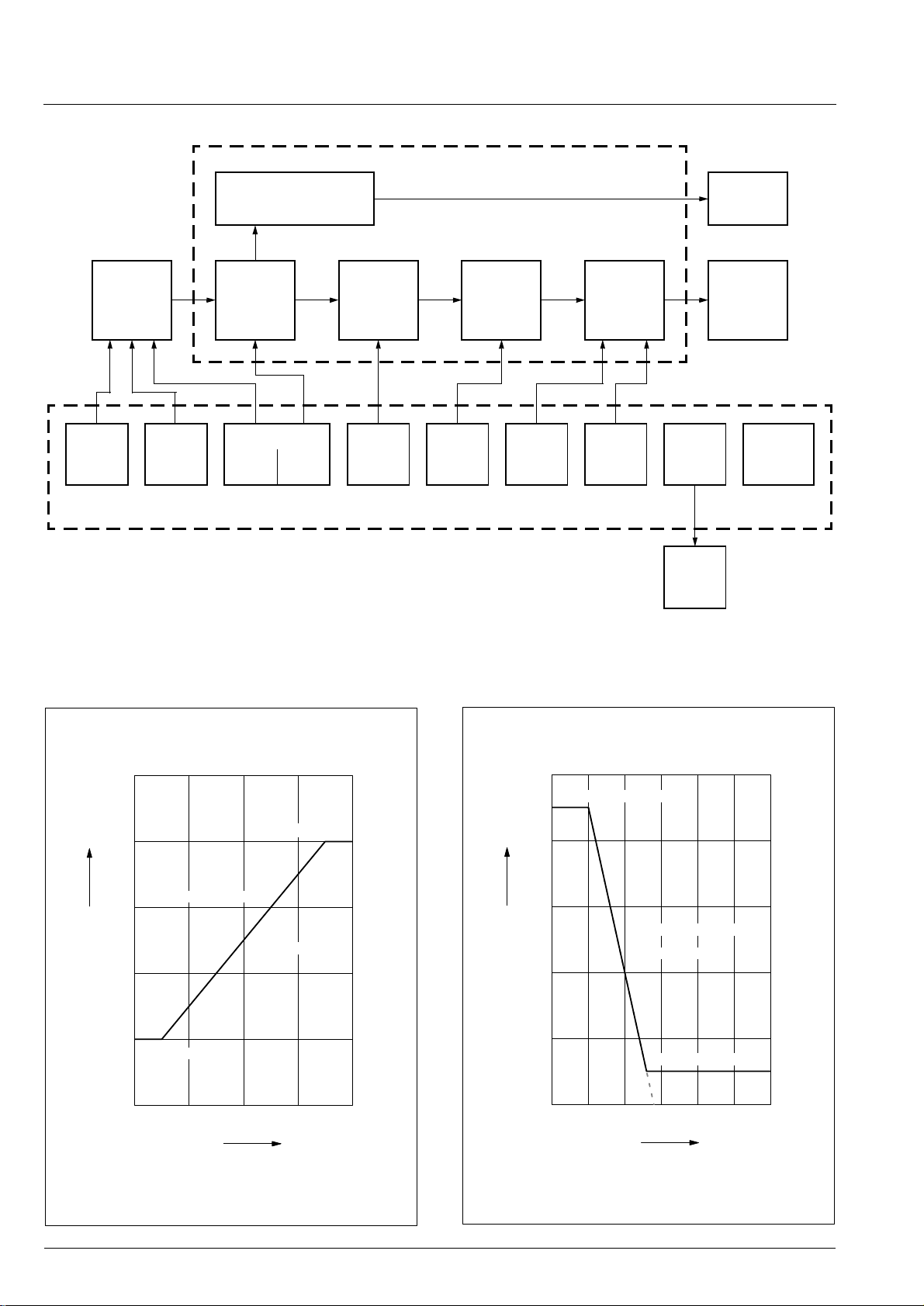
Fig. 2–4: Example for output characteristics
ADC-READOUT Register
14 bit
Digital Signal Processing
TC
6 bit
A/D
Converter
TCSQ
5 bit
Digital
Filter
MODE Register
RANGE
3 bit
FILTER
3 bit
Multiplier Adder Limiter D/A
SENSITIVITY LOW
14 bit
VOQ
11 bit
EEPROM Memory
Fig. 2–3: Details of EEPROM and Digital Signal Processing
CLAMP-
10 bit
CLAMPHIGH
11 bit
LOCKR
1 bit
Lock
Control
Digital
Output
Converter
Micronas
Registers
Range = 100 mT
Filter = 2 kHz
Sensitivity = –1.36
V
= –0.5 V
OQ
Clamp-low = 0.5 V
B
V
V
5
Clamp-high = 4.5 V
OUT
4
3
2
1
0
–150 –100 –50 0 50 100 150
Fig. 2–5: Example for output characteristics
mT
6 Micronas
Page 7
PRELIMINARY DATA SHEET HAL805
2.2. Digital Signal Processing and EEPROM
The DSP is the m ain par t of t his sensor and performs
the signal conditioning. The parameters for the DSP
are stored in the EEPROM r egisters. The details are
shown in Fig. 2–3.
Terminology:
SENSITIVITY: name of the register or register value
Sensitivity: name of the parameter
The EEPROM registers consist of three groups:
Group 1 contains the r egisters for the adaption of the
sensor to the magnetic system: MODE for selecting
the magnetic field range an d filter frequency, TC a nd
TCSQ for the temperature character istics of the magnetic sensitivity.
Group 2 contains the registers for defining the output
characteristics: SENSITIVITY, VOQ, CLAMP-LOW,
and CLAMP-HIGH. The output characteristic of the
sensor is defined by these 4 parameters (see Fig. 2–4
and Fig. 2–5 for examples).
– The parameter V
(Output Quiescent Voltage) cor-
OQ
responds to the output voltage at B = 0 mT.
– The parameter Sensitivity defines the magnetic sen-
sitivity:
∆V
Sensitivity =
OUT
∆B
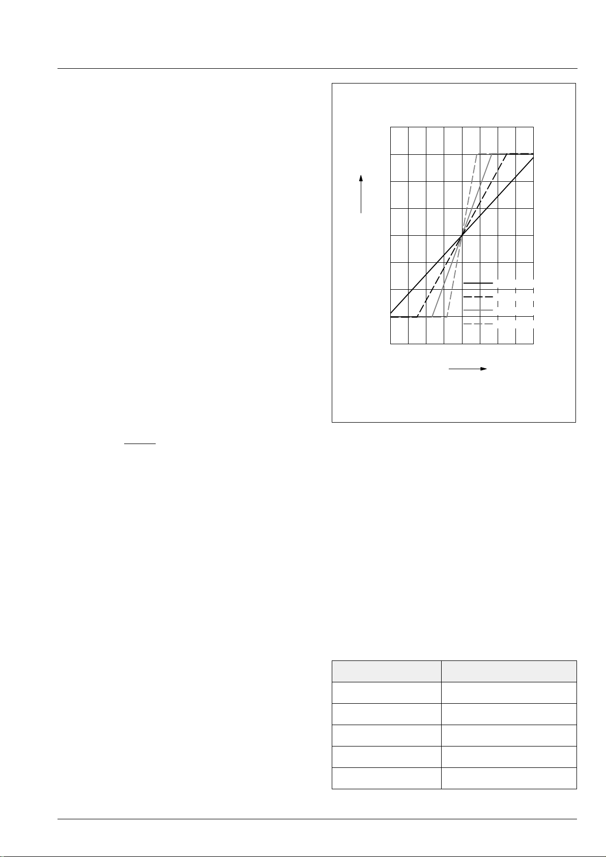
2000
1500
ADCREADOUT
1000
500
0
–500
–1000
–1500
–2000
–200–150–100–50 0 50 100 150 200
Fig. 2–6: Typical ADC-READOUT
versus magnetic field for filter = 2 kHz
Filter = 2 kHz
Range 150 mT
Range 90 mT
Range 60 mT
Range 30 mT
mT
B
– The output voltage can be calculated as:
∼ Sensitivity × B + V
V
OUT
OQ
The output voltage range can be clamped by setting
the registers CLAMP-LOW and CLAMP-HIGH in order
to enable failure detection (such as short-circuits to
or GND and open connections).
V
DD
Group 3 contains the Micronas registers and LOCK for
the locking of all r egisters. The Mi cronas regi sters are
programmed and locked during production and are
read-only for the customer. These registers a re used
for oscillator frequency tr imming, A/D converter offs et
compensation, and several other special settings.
An external magnetic field g enerates a Hall voltage on
the Hall plate. The ADC converts the amplified positive
or negative Hall voltage (operates with m agnetic no r th
and south poles at the branded side of the package) to
a digital value. Positive values correspond to a magnetic nor th pole on the branded side of the package.
The digital signa l is filt ered in th e inter nal low-pass fi lter and is readable in the ADC-READOUT register.
Depending on the programmable magnetic range of
the Hall IC, the operating range of the A/D converter i s
−30 mT...+30 mT up to −150 mT...+150 mT.
from
During further processing, the digital signal is multiplied with the se nsitivity factor, added to the quies cent
output voltage and limited according to the clamping
voltage. The result is converted to an analog signal
and stabilized by a push-pull output transistor stage.
The ADC-READOUT at any given magnetic field
depends on the programmed magnet ic field range but
also on the filter frequenc y. F ig. 2–6 shows the typical
ADC-READOUT values for the different magnetic field
ranges with the filter frequen cy set to 2 kHz. The rela tionship between the minimum and maximum ADCREADOUT values and the filter frequency setting is
listed in the following table.
Filter Frequency ADC-READOUT RANGE
80 Hz
160 Hz
500 Hz
1 kHz
2 kHz
−3968...3967
−1985...1985
−5292...5290
−2646...2645
−1512...1511
Micronas 7
Page 8
HAL805 PRELIMINARY DATA SHEET
Note: During application design, it should be taken
into consideration that the maximum and minimum
ADC-READOUT is not exceeded during calibration
and operation of the Hall IC. Consequently, the maximum and minimum magnetic fie lds that may occur in
the operational range of a s pecific application should
not saturate the A/D converter. Please note that the
A/D converter saturates at magnetic fi elds well above,
respectively below, the magnetic range limits. This
large safety band between specified magnetic range
and true operational range hel ps to avoid any saturation.
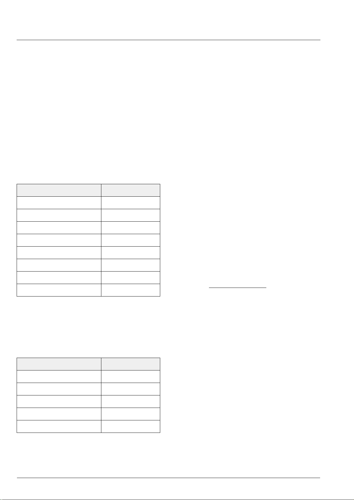
Range
The RANGE bits are the three lowest bits of the MODE
register; they define the magnetic field range of the
A/D converter.
Magnetic Field Range RANGE
−30 mT...30 mT 0
−40 mT...40 mT 4
−60 mT...60 mT 5
−75 mT...75 mT 1
−80 mT...80 mT 6
−90 mT...90 mT 2
−100 mT...100 mT 7
−150 mT...150 mT 3
TC and TCSQ
The temperature dependence of the magnetic sensitivity can be adapted to different magnetic materials in
order to compensate for the change of the magnetic
strength with temperature. The adaption is done by
programming the TC (Temperature Coefficient) and
the TCSQ registers (Quadratic Temperature Coefficient). Thereby , the slope and the curvature of the temperature dependence of the magnetic sensitivity can
be matched to the magne t and the sensor assembly.
As a result, the output voltage characteristic can be
fixed over the full temperature range. The sen sor can
compensate for linear temperature coefficients ranging
from about
dratic coefficients fr om about
−3100 ppm/K up to 400 ppm/K and qua-
−5 ppm/K² to 5 ppm/K².
Please refer to Section 4.3. on page 17 for the recommended settings for different linear temperature coefficients.
Sensitivity
The SENSITIVITY register contains the parameter for
the multiplier in the DSP. The Sensitivity is programmable between
−4 and 4. For V
= 5 V, the register
DD
can be changed in steps of 0.00049. Sensitivity = 1
corresponds to an increase of the output voltage by
if the ADC-READOUT increases by 2048.
V
DD
For all calculations, the di gi tal value from th e magnetic
field of the A/D converter is use d. This digital i nformation is readable from the ADC-READOUT register.
∆V
* 2048
Sensitivity =
∆ADC-READOUT * V
OUT
DD
VOQ
Filter
The VOQ register contains the parameter for the adder
The FILTER bits are the three highest bits of the
MODE register; they define the
−3 dB frequency of the
digital low pass filter.
in the DSP. V
magnetic field (B = 0 mT, respectively ADC-READOUT
= 0) and programmable from
is the output voltage without external
OQ
−V
up to VDD. For V
DD
DD
= 5 V, the register can be changed in steps of 4.9 mV.
−3 dB Frequency FILTER
80 Hz 0
160 Hz 1
500 Hz 2
1 kHz 3
2 kHz 4
Note: If V
is programmed to a negative voltage, the
OQ
maximum output voltage is limited to:
V
OUTmax
= VOQ + V
DD
For calibration in the system environment, a 2-point
adjustment procedure (see Section 2.3.) is recommended. The suitable Sensitivity and V
valu es for
OQ
each sensor can be ca lculated indi viduall y by this procedure.
8 Micronas
Page 9

PRELIMINARY DATA SHEET HAL805
Clamping Voltage
The output voltage range c an be clamped in order to
detect failures like shor ts to V
or GND or an open
DD
circuit.
The CLAMP-LOW register co ntains the parameter for
the lower limit. The lower clamping voltage is programmable between 0 V and V
/2. For VDD = 5 V, the reg-
DD
ister can be changed in steps of 2.44 mV.
The CLAMP-HIGH reg ister co ntains the param eter for
the upper limit. The upper clamping voltage is programmable between 0 V and V
. For VDD = 5 V, in
DD
steps of 2.44 mV.
LOCKR
By setting this 1-bit register, all registers will be locked,
and the sensor will no longer respond to any supply
voltage modulation.
Warning: This register cannot be reset!
ADC-READOUT
This 14-bit register delivers the actual digital value of
the applied magnetic field before the signal processing. This regist er can be read out and is the bas is for
the calibration pro cedure of the sensor in the s ystem
environment.
2.3. Calibration Procedure
2.3.1. General Procedure
For calibration in the syste m environmen t, the appli cation kit from Mi cron as i s rec om men ded . It contains the
hardware for the generation of the ser ial telegram for
programming and the corresponding software for the
input of the register values.
In this section, pro gramming of the sensor usin g this
programming tool is explained. Please refer to
Section 5. on page 19 for information ab out programming without this tool.
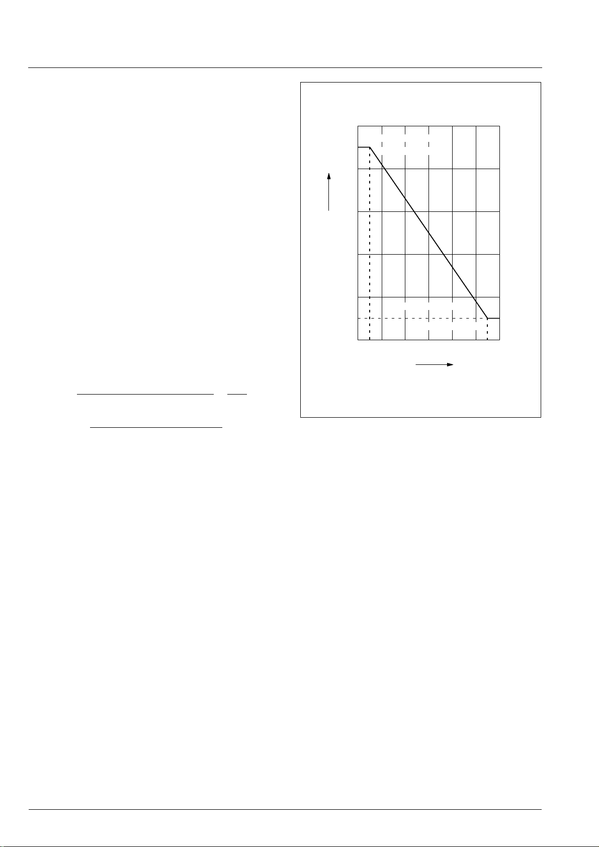
For the individual calibration of each sensor in the customer application, a two point adjustment is recommended (see Fig. 2–7 for an example). When using
the application ki t, the c alibratio n can b e done in thr ee
steps:
Step 1: Input of the registers which need not be
adjusted individually
The magnetic circuit, the magnetic material with its
temperature characteristics, the filter frequency, and
low and high clamping voltage are g iven for this application.
Therefore, the values of the following registers shou ld
be identical for all sensors of the customer application.
– FILTER
(according to the maximum signal frequency)
– RANGE
(according to the maximum magnetic field at the
sensor position)
– TC and TCSQ
(depends on the material of the magnet and the
other temperature dependencies of the application)
– CLAMP-LOW and CLAMP-HIGH
(according to the application requirements)
Write the appr opriate settings i nto the HAL 805 registers.
Micronas 9
Page 10
HAL805 PRELIMINARY DATA SHEET
Low clamping voltage ≤ V
OUT1,2
≤ High clamping voltage
V
OUT1
− V
OUT2
ADC-READOUT1 − ADC-READOUT2
Sensitivity =
V
DD
2048
*
ADC-READOUT1 * Sensitivity * V
DD
2048
VOQ = V
OUT1
−
Step 2: Calculation of VOQ and Sensitivity
The calibration points 1 and 2 can be set inside the
specified range. The corresponding values for V
and V
result from the application requirements.
OUT2
OUT1
For highest accuracy of the sensor, calibration points
near the minimum and maximum inp ut signal are recommended. The difference of the output voltage
between calibration point 1 and calibration point 2
should be more than 3.5 V.
Set the system to ca libration poin t 1 and read th e register ADC-READOUT. The result is the value ADCREADOUT1.
Now, set the system to calibration point 2, read the
register ADC-READOUT again, and get the value
ADC-READOUT2.
With these values and the target values V
, for the calibration points 1 and 2, re spectively,
V
OUT2
the values for Sensitivity and V
are calculated as:
OQ
OUT1
and
V
5
Clamp-high = 4.5 V
Calibration point 1
V
OUT
4
3
2
1
0
–30 –20 –10 0 10 20 30
Clamp-low = 0.5 V
Calibration point 2
Angle
Fig. 2–7: Example for output characteristics
°
This calculation has to be done individually for each
sensor.
Next, write the calculated values for Sensitivity and
into the IC for adjusting the sensor.
V
OQ
The sensor is now calibrated for the customer appl ication. However, the programming can be changed again
and again if necessary.
Step 3: Locking the Sensor
The last step is activating the LOCK function with the
“LOCK” command. The sensor is now locked and does
not respond to any programming or reading commands.
Warning: This register cannot be reset!
2.3.2. Calibration of the Angle Sensor
The following description explains the calibrati on procedure using an angle sensor as an example. The
required output characteristic is shown in Fig. 2–7.
– the angle range is from
−25° to 25°
Step 1: Input of the registers which need not be
adjusted individually
The register values f or the following registers ar e g iven
for all applications:
– FILTER
Select the filter frequency: 500 Hz
– RANGE
Select the magnetic field range: 30 mT
– TC
For this magnetic material: 6
– TCSQ
For this magnetic material: 14
– CLAMP-LOW
For our example: 0.5 V
– CLAMP-HIGH
For our example: 4.5 V
Enter these values in the software, and use the “write
and store” command for per manently writing the values in the registers.
– temperature coefficient of the magnet:
10 Micronas
−500 ppm/K
Page 11
PRELIMINARY DATA SHEET HAL805
Step 2: Calculation of VOQ and Sensitivity
There are two ways to calculate the values for V
OQ
and Sensitivity.
Manual Calculation:
Set the system to calibration point 1 (a ngle 1 =
−25°)
and read the register ADC- READOUT. For our example, the result is ADC-READOUT1 =
−2500.
Next, set the system to calibration point 2 (angle 2 =
25°), and read the register ADC-READO UT again. For
our example, the result is ADC-READOUT2 =
With these measurements and the targets V
4.5 V and V
V
are calculated as
OQ
Sensitivity =
= 4.5 V −
V
OQ
= 0.5 V, the values for Sensiti vity and
OUT2
4.5 V − 0.5 V
−2500 − 2350
−2500 * (−0.3378) * 5 V
2048
*
2048
5V
−0.3378
=
= 2.438 V
+2350.
OUT1
=
Software Calibration:
Use the menu CALIBRATE from the PC so ftware and
enter the values 4.5 V for V
Set the system to calibrat ion point 1 (angle 1 =
and 0.5 V for V
OUT1
OUT2
−25°),
hit the button “Read ADC-Readout1”, set the system to
calibration point 2 (angl e 2 = 25°), hi t the button “Read
ADC-Readout2”, and hit the button “Calculate”. The
software will then calculate the appropriate V
OQ
and
Sensitivity.
This calculation has to be done individually for each
sensor. Now, write the calculated values with the “write
and store” command into the HAL 805 for programming the sensor.
3. Specifications
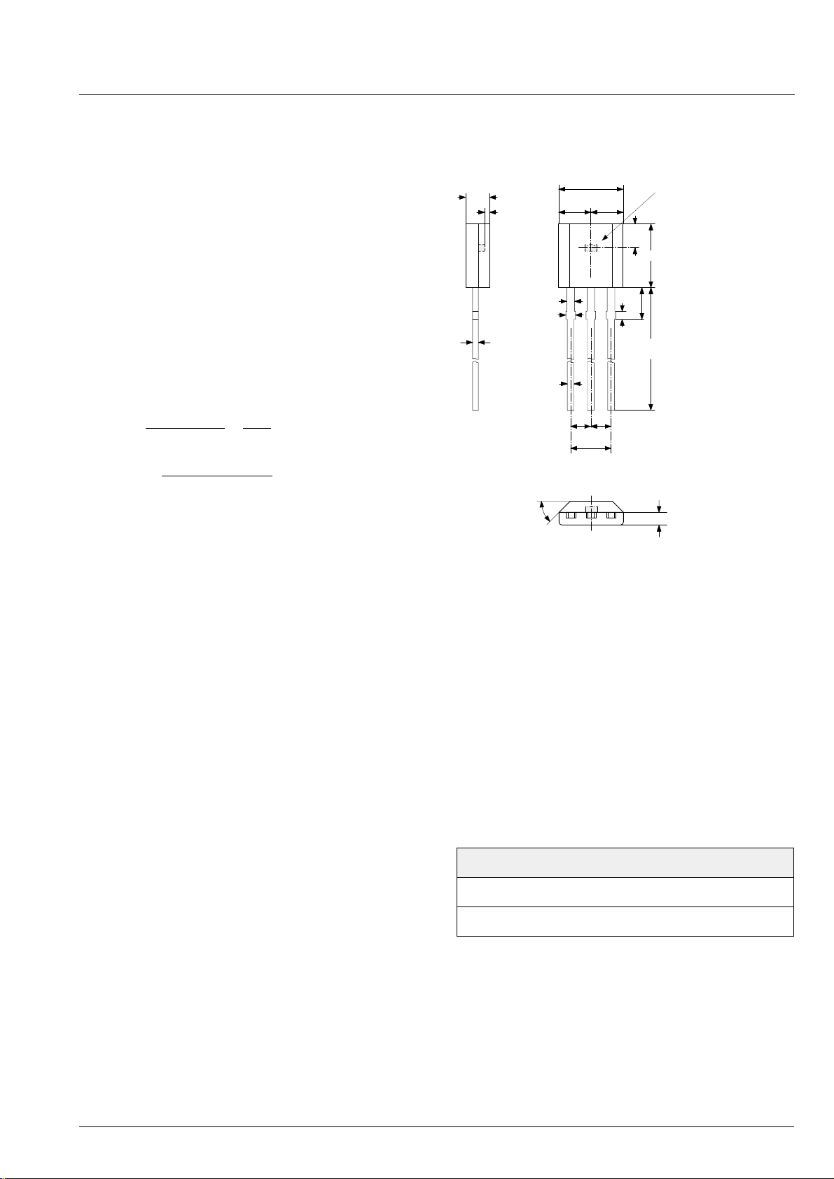
3.1. Outline Dimensions
±0.1
0.48
0.55
0.42
4.06
x2
x1
123
1.271.27
(2.54)
branded side
1.5
0.3
0.36
45°
SPGS0014-3-A/1E
.
Fig. 3–1:
±0.2
0.75
y
4.05
±0.2
2.1
13.0
min.
sensitive area
±0.1
0.8
Plastic Transistor Single Outline Package
(TO-92UT)
Weight approximately 0.14 g
Dimensions in mm
Note: A mechanical tolerance of
±50 µm applies t o all
dimensions where no tolerance is explicitly given.
3.2. Dimensions of Sensitive Area
0.25 mm x 0.25 mm
Step 3: Locking the Sensor
The last step is activating the LOCK function with the
3.3. Position of Sensitive Area
“LOCK” command. The sensor is now locked and does
not respond to any programming or reading com-
TO-92UT
mands.
x1 − x2/ 2 ≤ 0.2 mm
Warning: This register cannot be reset!
y = 1.5 mm
± 0.2 mm
Micronas 11
Page 12
HAL805 PRELIMINARY DATA SHEET
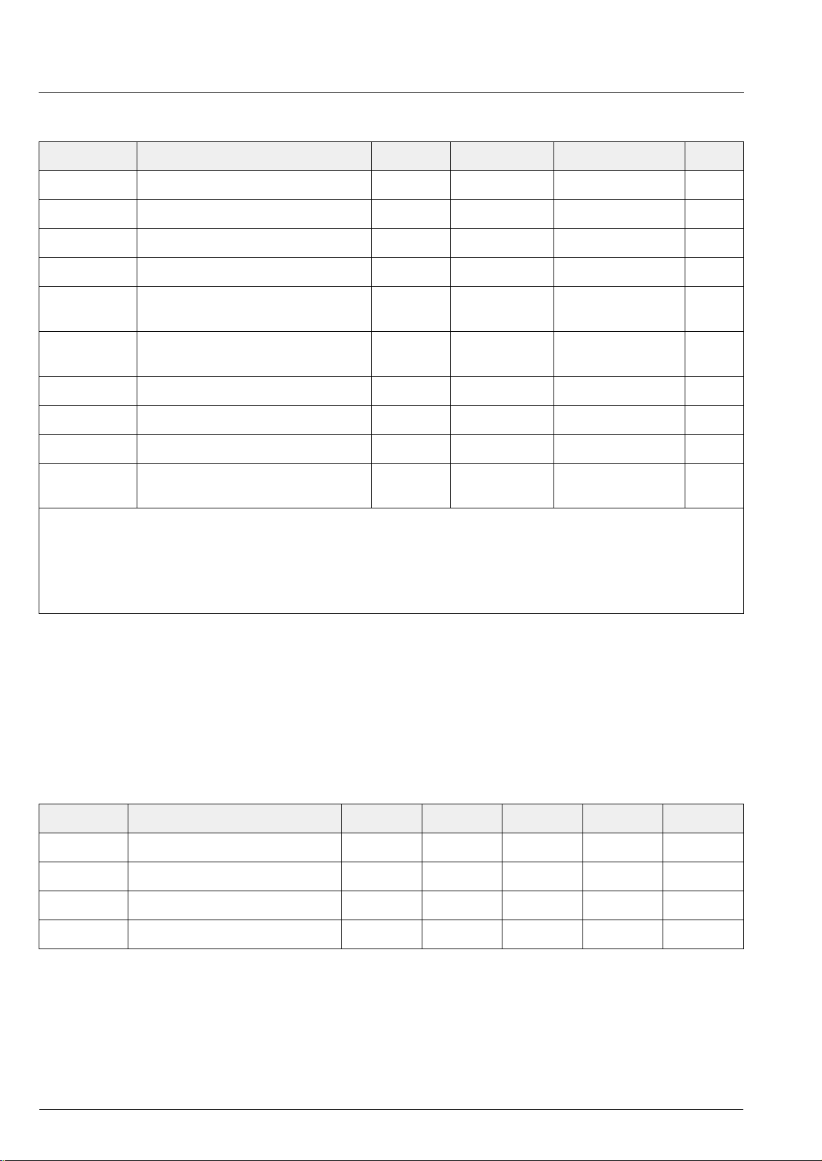
3.4. Absolute Maximum Ratings
Symbol Parameter Pin No. Min. Max. Unit
V
V
−I
I
V
V
DD
DD
Z
OUT
OUT
DD
− V
DD
Supply Voltage 1 −8.5 8.5 V
Supply Voltage 1 −14.4
Reverse Supply Current 1 − 50
Current through Protection Device 1 or 3 −300
Output Voltage 3 −5
Excess of Output V oltage
over Supply Voltage
I
OUT
t
Sh
T
S
T
J
1)
as long as T
2)
t < 10 min (V
3)
as long as T
4)
t < 2 ms
5)
t < 1000h
6)
internal protection resistor = 100 Ω
Continuous Output Current 3 −10 10 mA
Output Short Circuit Duration 3 − 10 min
Storage Temperature Range −65 150 °C
Junction Temperature Range −40
is not exceeded
Jmax
= −15 V for t < 1 min, V
DDmin
is not exceeded, output is not protected to external 14 V-line (or to −14 V)
Jmax
3,1 2 V
= 16 V for t < 1 min)
DDmax
−5
−40
1) 2)
4)
6)
6)
14.4
1)
300
8.5
14.4
170
150
3)
1) 2)
4)
3) 2)
5)
V
mA
mA
V
°C
°C
Stresses beyond those listed in the “Absolute Maximum Ratings” may cause permanent damage to the device. This
is a stress rating onl y. Functional operation of the device at these or any oth er condi tions beyond those indic ated i n
the “Rec ommended Operating Conditions/Character istics” of this specificati on is not i mplied. Ex posure to abs olute
maximum ratings conditions for extended periods may affect device reliability.
3.5. Recommended Operating Conditions
Symbol Parameter Pin No. Min. Typ. Max. Unit
V
I
OUT
R
C
DD
L
L
Supply Voltage 1 4.5 5 5.5 V
Continuous Output Current 3 −1 − 1mA
Load Resistor 3 4.5 −−kΩ
Load Capaci tance 3 0.33 10 1000 nF
12 Micronas
Page 13
PRELIMINARY DATA SHEET HAL805
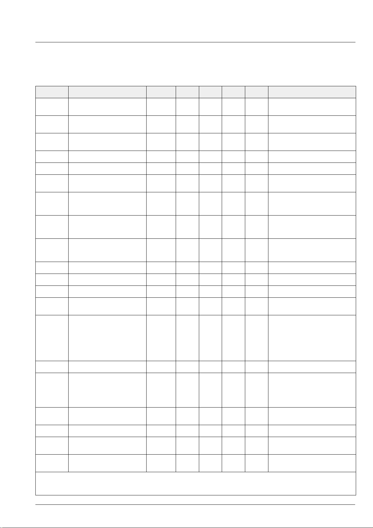
3.6. Electrical Characteristics
= −40 °C to +170 °C, VDD = 4.5 V to 5.5 V, after programming, as not otherwise specified in Conditions.
at T
J
Typical Characteristics for T
Symbol Parameter Pin No. Min. Typ. Max. Unit Conditions
= 25 °C and VDD = 5 V.
J
I
DD
V
DDZ
V
OZ
Supply Current
over Temperature Range
Overvoltage Protection
at Supply
Overvoltage Protection
at Output
Resolution 3 12 bit ratiometric to V
E
A
Accuracy Error over all 3 −202%R
INL Non-Linearity of Output Voltage
over Temperature
E
∆V
R
OUTCL
Ratiometric Error of Output
over Temperature
(Error in V
OUT
/ VDD)
Accuracy of Output Voltage at
Clamping Low Voltage over
Temperature Range
∆V
OUTCH
Accuracy of Output Voltage at
Clamping High Voltage over
Temperature Range
V
V
OUTH
OUTL
Output High Voltage 3 4.65 4.8 V V
Output Low Voltage 3 0.2 0.35 V V
1710mA
1 17.5 20 V IDD = 25 mA, TJ = 25 °C, t = 20 ms
31719.5VI
3 −1 0 1 % % of supply voltage
3
3
3
−101% V
−45 0 45 mV R
−45 0 45 mV R
= 10 mA, TJ = 25 °C, t = 20 ms
O
1)
DD
= 4.7 kΩ (% of supply voltage)
L
3)
- V
OUT2
> 2 V
DD
DD
= 5 V
= 5 V
OUT
OUT
≤ 1mA
≤ 1mA
OUT1
during calibration procedure
= 4.7 kΩ, V
L
= 4.7 kΩ, V
L
= 5 V, −1 mA ≤ I
DD
= 5 V, −1 mA ≤ I
DD
3)
f
ADC
f
ADC
t
r(O)
t
d(O)
t
POD
Internal ADC Frequency − 120 128 140 kHz TJ = 25 °C
Internal ADC Frequency over
Temperature Range
Response Time of Output 3 − 5
− 110 128 150 kHz V
10
4
2
1
8
4
2
ms
ms
ms
ms
= 4.5 V to 8.5 V
DD
3 dB Filter frequency = 80 Hz
3 dB Filter frequency = 160 Hz
3 dB Filter frequency = 500 Hz
3 dB Filter frequency = 2 kHz
C
= 10 nF, time from 10% to 90% of
L
final output voltage for a steplike
signal B
step
Delay Time of Output 3 0.1 0.5 ms CL = 10 nF
Power-Up Time (Time to reach
stabilized Output Voltage)
6
5
3
2
11
9
5
3
ms
ms
ms
ms
3 dB Filter frequency = 80 Hz
3 dB Filter frequency = 160 Hz
3 dB Filter frequency = 500 Hz
3 dB Filter frequency = 2 kHz
C
= 10 nF, 90% of V
L
BW Small Signal Bandwidth (−3dB) 3 − 2 − kHz BAC < 10 mT;
3 dB Filter frequency = 2 kHz
V
OUTn
R
OUT
R
thJA
TO-92UT
1)
Output DAC full scale = 5 V ratiometric, Output DAC offset = 0 V, Output DAC LSB = VDD/4096
2)
peak-to-peak value exceeded: 5%
3)
if more than 50% of the selected magnetic field range are used
Noise Output Voltage
pp
Output Resistance over Recommended Operating Range
Thermal Resistance Junction to
Soldering Point
3 − 36mV2) magnetic range = 90 mT
3 − 110Ω V
OUTLmax
≤ V
−−150 200 K/W
from 0 mT to B
OUT
≤ V
OUT
OUTHmin
max
Micronas 13
Page 14
HAL805 PRELIMINARY DATA SHEET
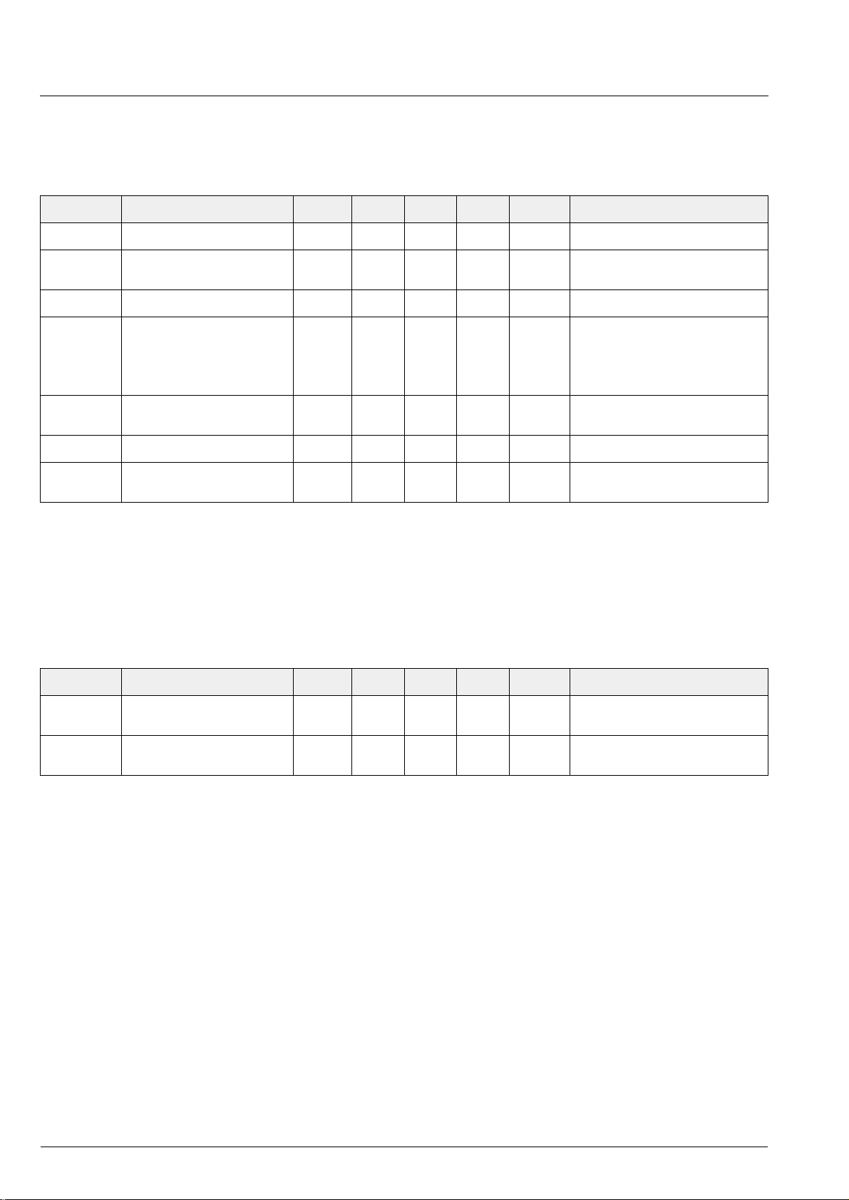
3.7. Magnetic Characteristics
= −40 °C to +170 °C, VDD = 4.5 V to 5.5 V, after programming, as not otherwise specified in Conditions.
at T
J
Typical Characteristics for T
Symbol Parameter Pin No. Min. Typ. Max. Unit Test Conditions
= 25 °C and VDD = 5 V.
J
B
Offset
∆B
Offset
B
Hysteresis
SR Magnetic Slew Rate 3
n
meff
f
Cflicker
f
Cflicker
Magnetic Offset 3 −101mTB = 0 mT, I
/∆T Magnetic Offset Change
due to T
J
Magnetic Hysteresis −20 0 20 µT Range = 30 mT, Filter = 500 Hz
Magnetic RMS Broadband
Noise
Corner Frequency of 1/f Noise 3 − 20 Hz B = 0 mT
Corner Frequency of 1/frms
Noise
3 − 10 −µT BW = 10 Hz to 2 kHz
3 − 100 Hz B = 65 mT, TJ = 25 °C
−15 0 15 µT/K B = 0 mT, I
− 2
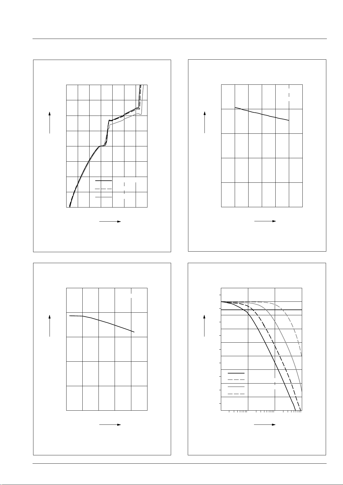
3.8. Open Circuit Detection
at T
= −40 °C to +170 °C, Typical Characteristics for TJ = 25 °C
J
4
12
25
50
= 0 mA, TJ = 25 °C
OUT
= 0 mA
OUT
− mT/ms Filter frequency = 80 Hz
Filter frequency = 160 Hz
Filter frequency = 500 Hz
Filter frequency = 1 kHz
Filter frequency = 2 kHz
Symbol Parameter Pin No. Min. Typ. Max. Unit Test Conditions
V
V
OUT
OUT
Output voltage
at open V
Output voltage at
open GND line
DD
line
3 000.2V V
34.74.85VV
= 5 V
DD
R
= 10 kΩ to GND
L
= 5 V
DD
R
= 10 kΩ to GND
L
14 Micronas
Page 15
PRELIMINARY DATA SHEET HAL805
3.9. Typical Characteristics
mA
20
15
I
DD
10
5
0
–5
–10
–15
T
= –40 °C
A
T
= 25 °C
A
TA=150 °C
–20
–15 –10 –50 5101520
V
DD
Fig. 3–2: Typical current consumption
versus supply voltage
mA
10
T
= 25 °C
A
V
= 5 V
DD
I
8
DD
6
4
2
0
V
–1.5 –1.0 –0.5 0.0 0.5 1.0 1.5
I
OUT
mA
Fig. 3–4: Typical current consumption
versus output current
mA
10
V
= 5 V
DD
I
8
DD
6
4
2
0
–50 0 50 100 150 200
T
A
Fig. 3–3: Typical current consumption
versus ambient temperature
dB
5
0
V
OUT
–5
–3
–10
–15
–20
–25
–30
–35
°
C
–40
10 100 1000 10000Hz
Filter: 80 Hz
Filter: 160 Hz
Filter: 500 Hz
Filter: 2 kHz
f
signal
Fig. 3–5: Typical output voltage
versus signal frequency
Micronas 15
Page 16
HAL805 PRELIMINARY DATA SHEET
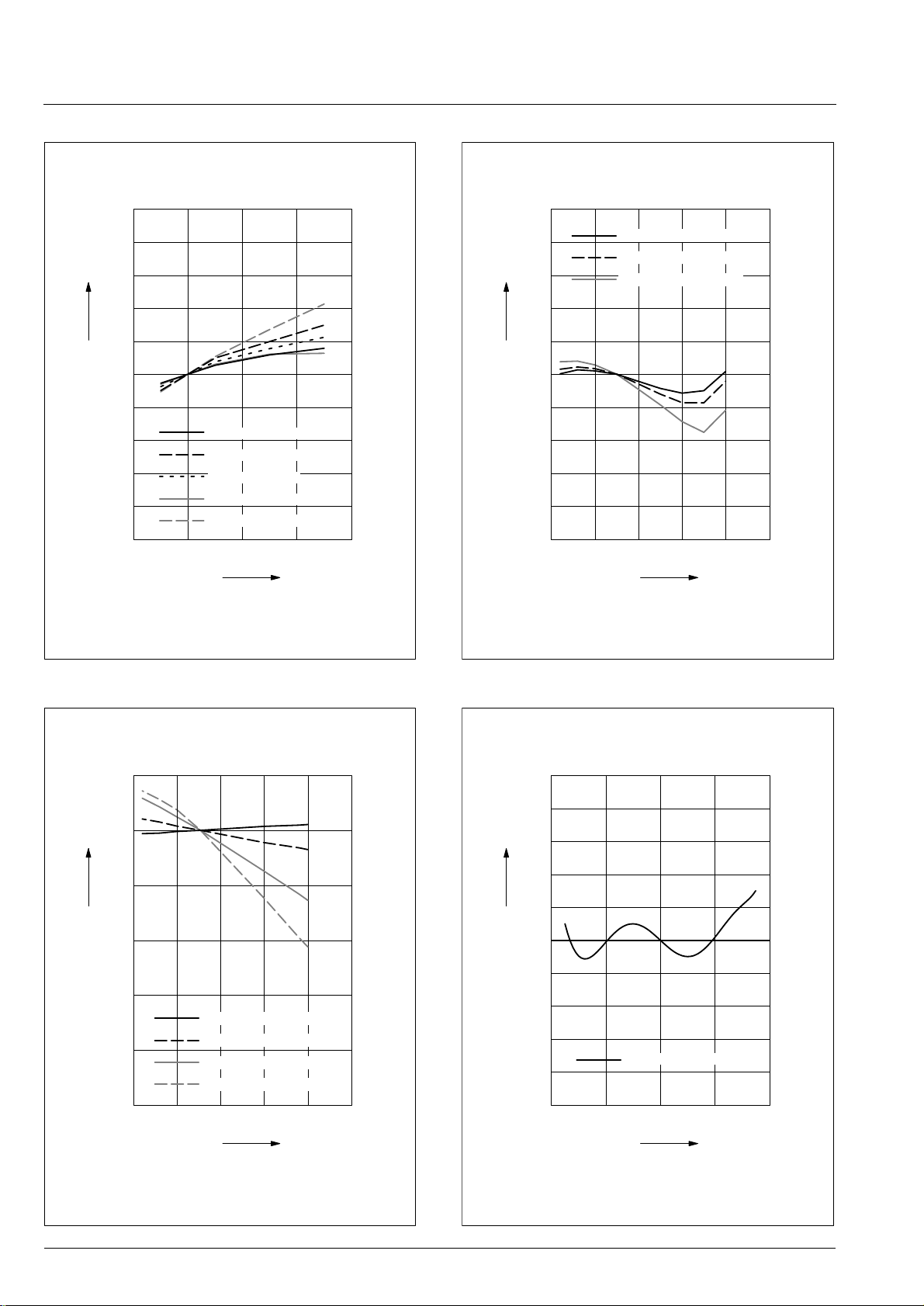
–1
–0.8
–0.6
–0.4
–0.2
–0.0
0.2
0.4
0.6
0.8
1.0
45678
V
%
V
DD
E
R
V
OUT/VDD
= 0.82
V
OUT/VDD
= 0.66
V
OUT/VDD
= 0.34
V
OUT/VDD
= 0.18
V
OUT/VDD
= 0.5
Fig. 3–6: Typical ratiometric error
versus supply voltage
0
20
40
60
80
100
120
–50 0 50 100 150 200
°C
%
T
A
1/sensitivity
TC = 16, TCSQ = 8
TC = 0, TCSQ = 12
TC = –20, TCSQ = 12
TC = –31, TCSQ = 0
Fig. 3–7: Typical 1/sensitivity
versus ambient temperature
mT
1.0
TC = 16, TCSQ = 8
TC = 0, TCSQ = 12
TC = –20, TCSQ = 12
B
0.8
Offset
0.6
0.4
0.2
–0.0
–0.2
–0.4
–0.6
–0.8
–1
–50 0 50 100 150 200
Fig. 3–8: Typical magnetic offset
versus ambient temperature
°C
T
A
%
1.0
0.8
INL
0.6
0.4
0.2
–0.0
–0.2
–0.4
–0.6
–0.8
–1
–40 –20 0 20 40
Range = 30 mT
mT
B
Fig. 3–9: Typical nonlinearity
versus magnetic field
16 Micronas
Page 17
PRELIMINARY DATA SHEET HAL805
4. Application Notes
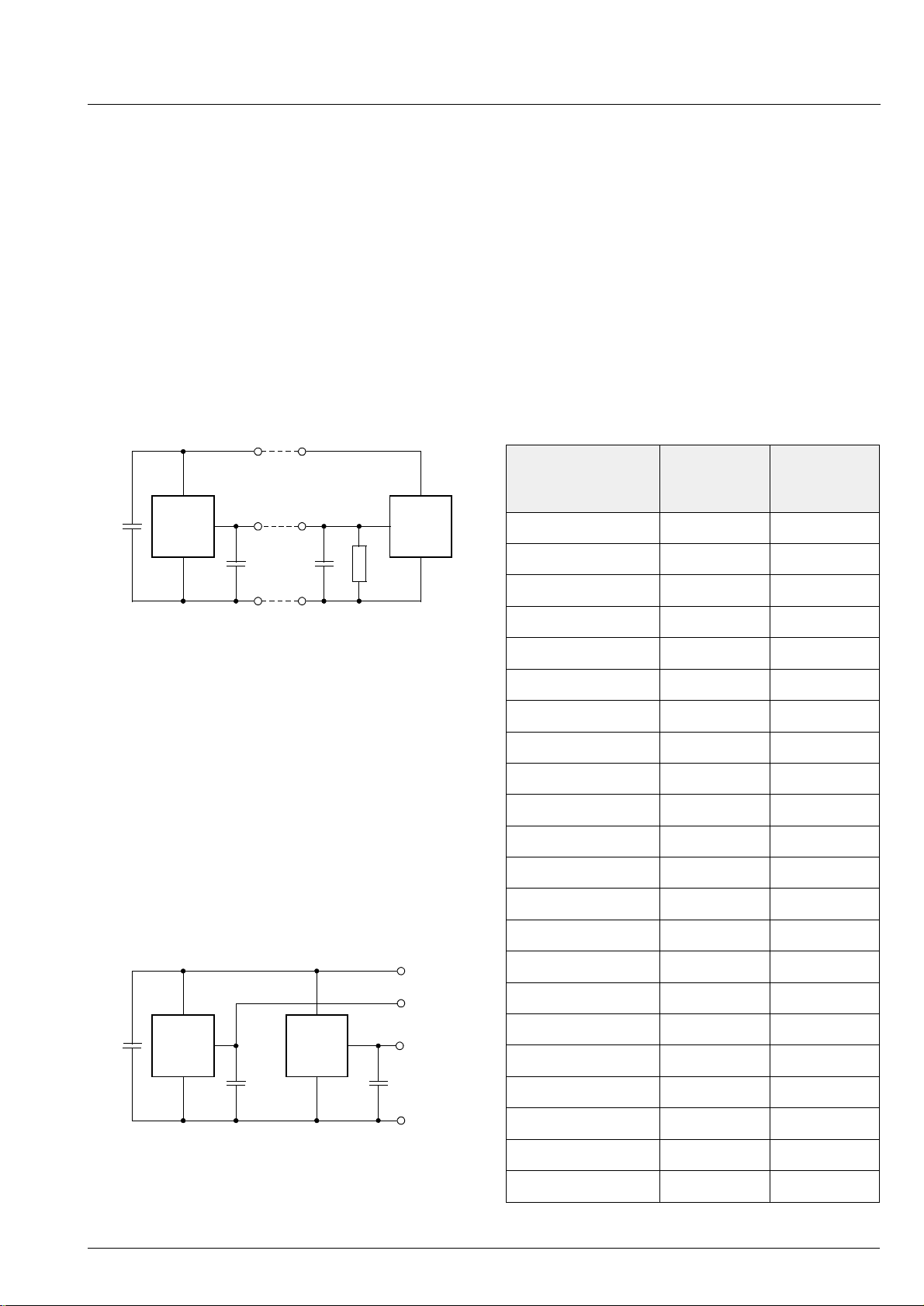
4.1. Application Circuit
For EMC protection, it is recommended to connect one
ceramic 4.7 nF capacitor each between ground and
the supply voltage, respecti vely the o utput voltage pin.
In addition, the input of the controller unit should be
pulled-down with a 4.7 kOhm resistor and a ceramic
4.7 nF capacitor.
Please note that during programming , the sensor will
be supplied repeatedl y with the programming voltage
of 12 V for 100 ms. All components conn ected to the
line at this time must be able to resist this voltage.
V
DD
V
DD
OUT
GND
4.7 k
µ
C
Ω
4.7 nF
HAL805
4.7 nF 4.7 nF
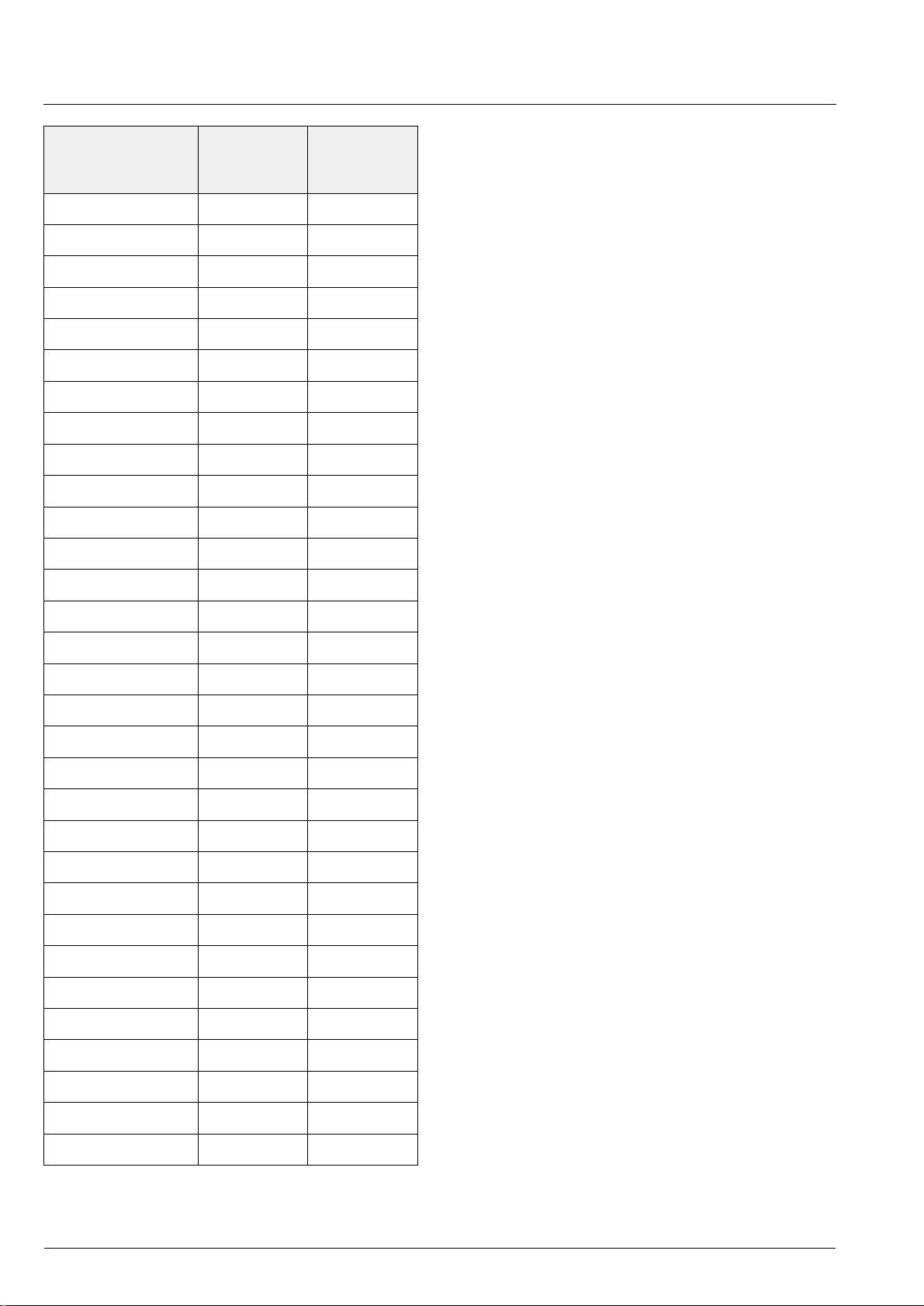
4.3. Temperature Compensation
The relationship between the temperature coefficient
of the magnet and the corresponding TC an d TCSQ
codes for linear compens ation is given in the following
table. In addition to the linear chan ge of the magnetic
field with temperature, the cu rvature can be adjusted
as well. For this purpose, other TC and TCSQ combi nations are required whi ch are not shown in the table.
Please contact MICRONAS for more detailed information on this higher order temperature compensation.
The HAL 800 and HAL 805 contain the same temperature compensation cir cuits. If an o ptimal s etting for the
HAL 800 is already available, the same settings may
be used for the HAL 805.
Temperature
TC TCSQ
Coefficient of
Magnet (ppm/K)
400 31 6
300 28 7
200 24 8
Fig. 4–1: Recommended application circuit
4.2. Use of two HAL 805 in Parallel
Two different HAL 805 sens ors which are operated in
parallel to the same supply and ground line can be
programmed individually. In order to select the IC
which should be programmed, bo th Hal l ICs ar e inac tivated by the “Deactivate” command on the common
supply line. Then, the appropri ate IC is activated by an
“Activate” pulse on its output . Only the activated sensor will react to all following read, write, and program
commands. If the second IC has to be programmed,
the “Deactivate” command is sent agai n, and the second IC can be selected.
V
DD
OUT A & Select A
OUT B & Select B
10 nF
HAL 805
Sensor A Sensor B
HAL 805
100 21 9
01810
−50 17 10
−90 16 11
−130 15 11
−170 14 11
−200 13 12
−240 12 12
−280 11 12
−320 10 13
−360 9 13
−410 8 13
−450 7 13
−500 6 14
−550 5 14
4.7 nF
4.7 nF
GND
−600 4 14
−650 3 14
Fig. 4–2: Parallel operation of two HAL 805
−700 2 15
−750 1 15
Micronas 17
Page 18
HAL805 PRELIMINARY DATA SHEET
Temperature
TC TCSQ
Coefficient of
Magnet (ppm/K)
−810 0 15
−860 −116
−910 −216
−960 −316
−1020 −417
−1070 −517
−1120 −617
−1180 −718
−1250 −818
−1320 −919
−1380 −10 19
−1430 −11 20
−1500 −12 20
−1570 −13 20
−1640 −14 21
−1710 −15 21
4.4. Undervoltage Behavior
In a voltage range below 4.5 V to approximately 3.5 V,
the operation of the HAL 805 is typically given and predictable for the most sensors. So me of the parameters
may be out of the speci ficat ion . B el ow abo ut 3.5 V, the
digital processing is reset. If the supply voltage once
again rises a bove about 3.5 V, a s tar tup time of about
µs elapses for the digital processing to occur. As
20
long as the supply voltage is still above about 2.8 V,
the analog output is kept at its last valid value ratiometric to V
. Below about 2.5 V, the entire sensor will
DD
reset.
4.5. Ambient Temperature
Due to the intern al power dissipation, th e temperature
on the silicon chi p (junction temperature T
) is higher
J
than the temperature outside the package (ambient
temperature T
= TA + ∆T
T
J
).
A
At static conditions, the following equation is valid:
∆T = I
* VDD * R
DD
thJA
For typical values, use the typical parameters. For
worst case calculation, use the max. parameters for
I
and Rth, and the max. value for VDD from the appli-
DD
cation.
−1780 −16 22
−1870 −17 22
−1950 −18 23
−2030 −19 23
−2100 −20 24
−2180 −21 24
−2270 −22 25
−2420 −24 26
−2500 −25 27
−2600 −26 27
−2700 −27 28
−2800 −28 28
−2900 −29 29
−3000 −30 30
−3100 −31 31
For V
temperature difference
For all sensors, the junction tem perature T
fied. The maximum ambient temperature T
= 5.5 V, Rth = 200 K/W and IDD = 10 mA the
DD
∆T = 11 K.
is speci-
J
can be
Amax
calculated as:
T
Amax
= T
Jmax
−∆T
4.6. EMC and ESD
The HAL 805 is designe d for a stabilized 5 V suppl y.
Interferences and disturbances conducted along the
12 V onboard system (product standards DIN40839
part 1 or ISO 7637 part 1) are not relevant for these
applications.
For applications with disturbances by capacitive or
inductive coupling on the supply line or radiat ed disturbances, the application circuit shown in Fig. 4–1 is recommended. Applications with this arrangement
passed the EMC tests acc ording to the product standards DIN 40839 pa rt 3 (Ele ctrical transient transmission by capacitive or inductive coupling) and part 4
(Radiated disturbances).
Please contact M icronas for the detailed investigation
reports with the EMC and ESD results.
18 Micronas
Page 19
PRELIMINARY DATA SHEET HAL805
5. Programming of the Sensor
5.1. Definition of Programming Pulses
The sensor is addre ssed by modulating a serial telegram on the supply voltage. The se nsor answers with
a serial telegram on the output pin.
The bits in the serial telegram have a different bit time
for the V
V
-line is defined through the length of the S ync Bit
DD
-line and the output. The bit time for the
DD
at the beginning of each tel egram. The bit time for the
output is defined through the Acknowledge Bit.
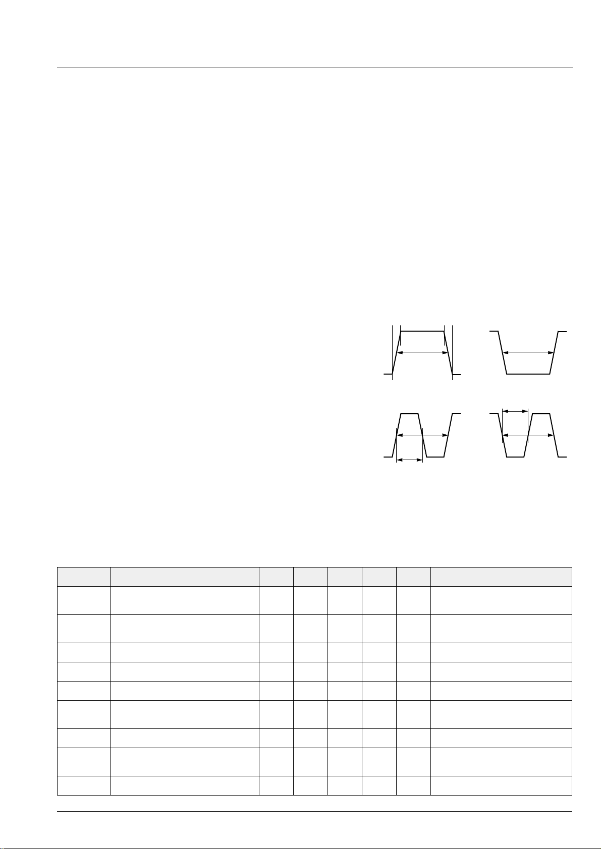
A logical “0” is coded as no voltage change within the
bit time. A logical “1” is coded as a voltage change
between 50% and 80% of the bit time. After each bit, a
voltage change occurs.
5.2. Definition of the Telegram
Each telegram starts with the Sync Bit (logical 0), 3
bits for the Command (COM), th e Comm and Parity B it
(CP), 4 bits for the Address ( ADR), and the Address
Parity Bit (AP).
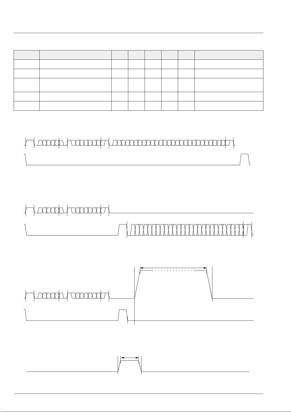
– Read a register (see Fig. 5–3)
After evaluating this command, the sensor answers
with the Acknowledge Bit, 14 Data Bits, and the
Data Parity Bit on the output.
– Programming the EEPROM cells (see Fig. 5–4)
After evaluating this command, the sensor answers
with the Acknowledge Bit. After the delay time t
the supply voltage ris es up to the p ro gramming voltage.
– Activate a sensor (see Fig. 5–5))
If more than one sensor is conne cted to the supply
line, selection ca n be done by first deactivating all
sensors. The output of all sensors will be pulled to
ground by the internal 10 k
Ω resistors. With an Acti-
vate pulse on the appropria te output pin, an ind ividual sensor can be selected. A ll following co mm and s
will only be accepted from the activated sensor.
logical 0
V
V
DDH
DDL
t
r
t
f
t
p0
or
t
p0
,
w
There are 4 kinds of telegrams:
V
V
DDH
DDL
t
p0
t
p1
– Write a register (see Fig. 5–2)
After the AP Bit, follow 14 Data Bits (DAT) and the
Data Parity Bit (DP). If the telegram is valid and the
command has been proces sed, th e sens or answers
logical 1
with an Acknowledge Bit (logical 0) on the output.
Fig. 5–1: Definition of logical 0 and 1 bit
Table 5–1: Telegram parameters
Symbol Parameter Pin Min. Typ. Max. Unit Remarks
V
V
t
t
t
r
f
p0
DDL
DDH
Supply Voltage for Low Level
during Programming
Supply Voltage for High Level
during Programming
Rise time 1 0.05 ms
Fall time 1 0.05 ms
Bit time on V
DD
155.66V
16.88.08.5V
1 1.7 1.75 1.8 ms tp0 is defined through the Sync Bit
t
p1
t
or
p0
t
pOUT
t
p1
V
DDPROG
t
PROG
Bit time on output pin 3 2 3 4 ms t
Voltage Change for logical 1 1, 3 50 65 80 % % of t
Supply Voltage for
Programming the EEPROM
Programming Time for EEPROM 1 95 100 105 ms
1 11.95 12 12.1 V
pOUT
Acknowledge Bit
is defined through the
or t
p0
pOUT
Micronas 19
Page 20
HAL805 PRELIMINARY DATA SHEET
Table 5–1: Telegram parameters, continued
Symbol Parameter Pin Min. Typ. Max. Unit Remarks
t
rp
t
fp
t
w
V
act
t
act
Rise time of programming voltage 1 0.2 0.5 1 ms
Fall time of programming voltage 1 0 1 ms
Delay time of programming voltage
10.50.71ms
after Acknowledge
Voltage for an Activate pulse 3 3 4 5 V
Duration of an Activate pulse 3 0.05 0.1 0.2 ms
WRITE
Sync COM CP ADR AP DAT DP
V
DD
V
OUT
Fig. 5–2: Telegram for coding a Write command
READ
Sync COM CP ADR AP
Acknowledge
V
DD
V
OUT
Fig. 5–3: Telegram for coding a Read command
V
DDPROG
ERASE, PROM, LOCK, and LOCKI
Sync COM CP ADR
V
DD
AP
Acknowledge
V
OUT
t
w
Fig. 5–4: Telegram for coding the EEPROM programming
DA T DPAcknowledge
t
rp
t
PROG
t
fp
t
V
OUT
t
r
V
ACT
ACT
t
f
Fig. 5–5: Activate pulse
20 Micronas
Page 21
PRELIMINARY DATA SHEET HAL805
5.3. Telegram Codes
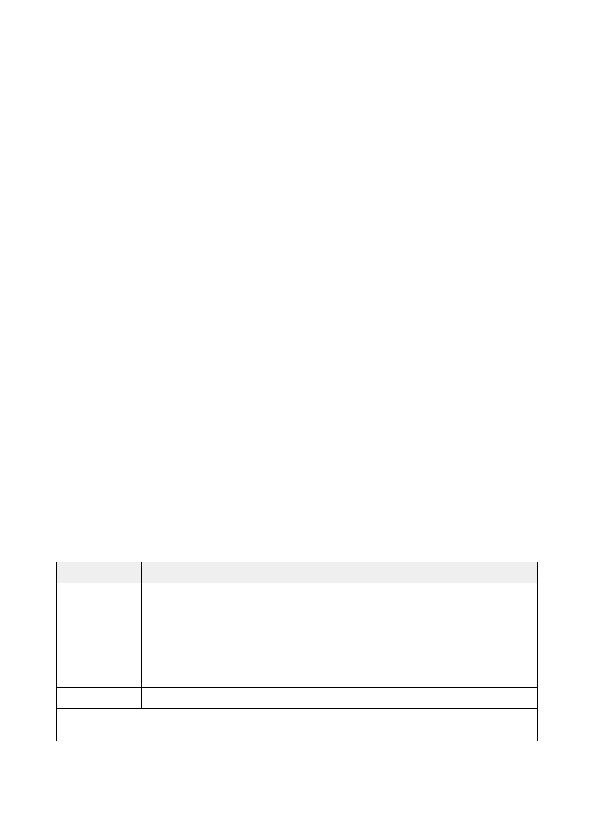
Sync Bit
Each telegram star ts wi th the Sync Bit. Thi s log ical “0”
pulse defines the exact timing for t
p0
.
Command Bits (COM)
The Command code contains 3 bits and is a binary
number. Table 5–2 shows the available commands
and the corresponding codes for the HAL 805.
Command Parity Bit (CP)
This parity bit is “1” if the number of zeros within the 3
Command Bits is uneven. The parity bit is “0”, if the
number of zeros is even.
Address Bits (ADR)
The Address code contains 4 bits and is a binary number. Table 5–3 shows the available addresses for the
HAL 805 registers.
Data Bits (DAT)
The 14 Data Bits contain the register information.
The registers use different number formats for the
Data Bits. These formats are explained in Section 5.4.
In the Write command, the last bits are valid. If, for
example, the TC register (6 bits) is written, only the
last 6 bits are valid.
In the Read command, the first bits are valid. If, for
example, the TC register (6 bits) is read, only the first 6
bits are valid.
Data Parity Bit (DP)
This parity bit is “1” if the number of zeros within the
binary num ber is even. The p arity bit is “0” if the number of zeros is uneven.
Acknowledge
After each telegram, the output answers with the
Acknowledge signal. This logical “0” pulse defines the
exact timing for t
pOUT
.
Address Parity Bit (AP)
This parity bit is “1” if the number of zeros within the 4
Address bits is uneven. The par ity b it is “0” if the number of zeros is even.
Table 5–2: Available commands
Command Code Explanation
READ 2 read a register
WRITE 3 write a register
PROM 4 program all nonvolatile registers (except the lock bits)
ERASE 5 erase all nonvolatile registers (except the lock bits)
LOCKI 6 lock MICRONAS lockable register
LOCK 7 lock the whole device and switch permanently to the analog-mode
Please note:
The MICRONAS lock bit (LOCKI) has already been set during production and cannot be reset.
Micronas 21
Page 22
HAL805 PRELIMINARY DATA SHEET
5.4. Number Formats
Binary number:
The most significant bit i s given as first, the least significant bit as last digit.
Example:
Signed binary number:
The first digit represents the sign of the following
binary number (1 for negative, 0 for positive sign).
Example:
101001 represents 41 decimal.
0101001 represents +41 decimal
1101001 represents −41 decimal
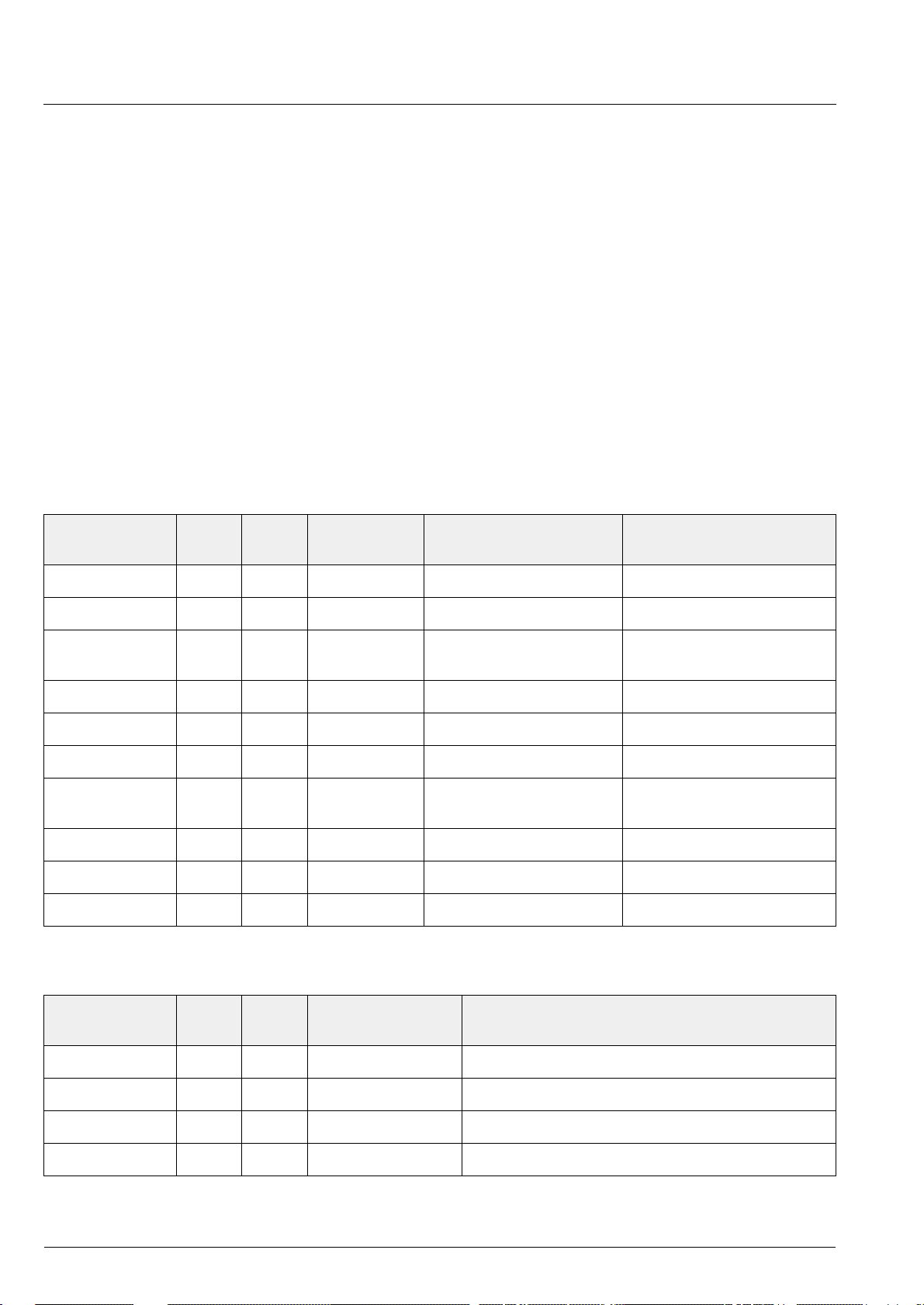
Table 5–3: Available register addresses
Register Code Data
Bits
Format Customer Remark
Two-complementary number:
The first digit of positive numbers is “0”, the rest of the
number is a binary number. Negative numbers start
with “1”. In or der to calc ulate the ab solut e value of the
number, calculate the complement of the remaining
digits and add “1”.
Example:
0101001 represents +41 decimal
1010111 represents −41 decimal
CLAMP-LOW 1 10 binary read/write/program Low clamping voltage
CLAMP-HIGH 2 11 binary read/write/program High clamping voltage
VOQ 3 11 two compl.
binary
SENSITIVITY 4 14 signed binary read/write/program
MODE 5 6 binary read/write/program Range and filter settings
LOCKR 6 1 binary lock Lock Bit
ADC-READOUT 7 14 two compl.
binary
TC 11 6 signed binary read/write/program
TCSQ 12 5 binary read/write/program
DEACTIVATE 15 12 binary write Deactivate the sensor
MICRONAS registers (read only for customers)
Register Code Data
Bits
Format Remark
read/write/program
read
OFFSET 8 4 two compl. binary ADC offset adjustment
FOSCAD 9 5 binary Oscillator frequency adjustment
SPECIAL 13 6 special settings
IMLOCK 14 1 binary Lock Bit for the Micronas registers
22 Micronas
Page 23

PRELIMINARY DATA SHEET HAL805
5.5. Register Information
CLAMP-LOW
– The register range is from 0 up to 1023.
– The register value is calculated by:
Low Clamping Voltage
V
DD
* 2048CLAMP-LOW =
CLAMP-HIGH
– The register range is from 0 up to 2047.
– The register value is calculated by:
High Clamping Voltage
V
DD
VOQ
– The register range is from
−1024 up to 1023.
– The register value is calculated by:
V
OQ
* 1024VOQ =
V
DD
ADC-READOUT
– This register is read only.
– The register range is from
−8192 up to 8191.
DEACTIVATE
– This register can only be written.
– The register has to be written with 2063 decimal
(80F hexadecimal) for the deactivation.
– The sensor can be r eset with an Activate pulse on
the output pin or by switching off and o n the suppl y
voltage.
5.6. Programming Information
* 2048CLAMP-HIGH =
If the content of any register (except the lock registers)
is to be changed, th e desired value must first be written into the correspond ing RAM registe r. Before reading out the RAM register again, the register value must
be permanently stored in the EEPROM.
Permanently storin g a value in the EEP ROM is done
by first sending an ERASE command followed by
sending a PROM command. The address within the
ERASE and PROM commands is not important.
ERASE and PROM act on all registers in parallel.
SENSITIVITY
– The register range is from
−8192 up to 8191.
– The register value is calculated by:
SENSITIVITY =
Sensitivity
2048
TC and TCSQ
– The TC register range is from
−31 up to 31 .
– The TCSQ register range is from 0 up to 31.
Please refer Section 4.2. on page 17 for the recom-
mended values.
MODE
– The register range is f rom 0 up to 63 and conta ins
the settings for FILTER and RANGE:
MODE = FILTER * 8 + RANGE
If all HAL 805 registers are to be cha nged, all writing
commands can be sent one after the other, followed by
sending one ERASE and PROM command at the end.
Please refer Section 2.2. on page 7 for the available
FILTER and RANGE values.
Micronas 23
Page 24

HAL805 PRELIMINARY DATA SHEET
6. Data Sheet History
1. Preliminary data sheet:
“HAL805 Programmable Linear Hall Effect Sensor”,
Feb. 2, 2000, 6251-513-1PD.
First release of the preliminary data sheet.
Micronas GmbH
Hans-Bunte-Strasse 19
D-79108 Freiburg (Germany)
P.O. Box 840
D-79008 Freiburg (Germany)
Tel. +49-761-517-0
Fax +49-761-517-2174
E-mail: [email protected]
Internet: www.micronas.com
Printed in Germany
Order No. 6251-513-1PD
All information and data contained in this data sheet are without any
commitment, are not to be considered as an offer for conclusion of a
contract, nor shall they be construed as to create any liability. Any new
issue of this data sheet invalidates previous issues. Product availability
and delivery are exclusively subject to our respective order confirmation
form; the same applies to orders based on development samples delivered. By this publication, Micronas GmbH does not assume responsibility for patent infr ingements or other right s of third parties whic h may
result from its use.
Further, Micronas GmbH reserves the right to revise this publication and
to make changes to its conte nt, at any t ime, withou t obligatio n to noti fy
any person or entity of such revisions or changes.
No part of this publication may be reproduced, photocopied, stored on a
retrieval system, or transmitted without the express written consent of
Micronas GmbH .
24 Micronas
 Loading...