

Page 1
3-161
Features
• Programmability
• High Rate Slew. . . . . . . . . . . . . . . . . . . . . . . . . . . 30V/µs
• Wide Gain Bandwidth . . . . . . . . . . . . . . . . . . . . . 40MHz
• High Gain . . . . . . . . . . . . . . . . . . . . . . . . . . . . . . 150kV/V
• Low Offset Current . . . . . . . . . . . . . . . . . . . . . . . . . .5nA
• High Input Impedance . . . . . . . . . . . . . . . . . . . . . . 30MΩ
• Single Capacitor Compensation
• DTL/TTL Compatible Inputs
Applications
• Thousands of Applications; Program
- Signal Selection/Multiplexing
- Operational Amplifier Gain
- Oscillator Frequency
- Filter Characteristics
- Add-Subtract Functions
- Integrator Characteristics
- Comparator Levels
Description
THA-2400/04/05 comprise a series of four-channel
programmable amplifiers providing a level of versatility
unsurpassed by any other monolithic operational amplifier.
Versatility is achieved by employing four input amplifier
channels, any one (or none) of which may be electronically
selected and connected to a single output stage through
DTL/TTL compatible address inputs. The device formed by
the output and the selected pair of inputs is an op amp which
delivers excellent slew rate, gain bandwidth and power
bandwidth performance. Other advantageous features for
these dielectrically isolated amplifiers include high voltage
gain and input impedance coupled with low input offset
voltage and offset current. External compensation is not
required on this device at closed loop gains greater than 10.
Each channel of the HA-2400/04/05 can be controlled and
operated with suitable feedback networks in any of the
standard op amp configurations. This specialization makes
these amplifiers excellent components for multiplexing signal
selection and mathematical function designs. With 30V/µs
slew rate, 40MHz gain bandwidth and 30MΩ input
impedance these devices are ideal building blocks for signal
generators, active filters and data acquisition designs.
Programmability, coupled with 4mV typical offset voltage and
5nA offset current, makes these amplifiers outstanding
components for signal conditioning circuits.
During Disable Mode V
OUT
goes to V-. For high output
impedance during Disable, see HA2444.
For further design ideas, see Application Note AN514.
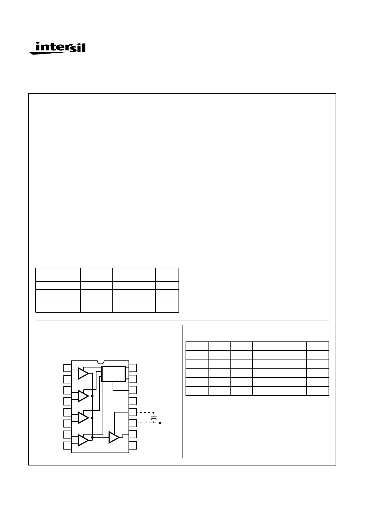
Pinout
HA-2400/04 (CERDIP)
HA-2405 (CERDIP, PDIP)
TOP VIEW)
Ordering Information
PART NUMBER
TEMP.
RANGE (oC) PACKAGE
PKG.
NO.
HA1-2400-2 -55 to 125 16 Ld CERDIP F16.3
HA1-2404-4 -25 to 85 16 Ld CERDIP F16.3
HA1-2405-5 0 to 75 16 Ld CERDIP F16.3
HA3-2405-5 0 to 75 16 Ld PDIP E16.3
14
15
16
9
13
12
11
10
1
2
3
4
5
7
6
8
3
OUTPUT AMP
ENABLE
D0
D1
GND
COMP
V+
OUT
V-
4
1
2
+IN3
-IN3
+IN4
-IN4
-IN1
+IN1
+IN2
-IN2
3
DECODE
CONTROL
+
-
+
-
+
-
+
-
TRUTH TABLE
D1 D0 EN SELECTED CHANNEL D1
LLH 1 L
LHH 2 L
HLH 3 H
HHH 4 H
X X L None, V
OUT
goes to V- X
November 1996
HA-2400, HA-2404,
HA-2405
40MHz, PRAM Four Channel
Programmable Amplifiers
File Number 2891.2
CAUTION: These devices are sensitive to electrostatic discharge; follow proper IC Handling Procedures.
1-888-INTERSIL or 321-724-7143 | Copyright © Intersil Corporation 1999
Page 2
3-162
Absolute Maximum Ratings T
A
=25oC Thermal Information
Voltage Between V+ and V- Terminals . . . . . . . . . . . . . . . . . . 45.0V
Differential Input Voltage. . . . . . . . . . . . . . . . . . . . . . . . . . . V
SUPPLY
Digital Input Voltage . . . . . . . . . . . . . . . . . . . . . . . -0.76V to +10.0V
Output Current . . . . . . . . . . . Short Circuit Protected, ISC <±33mA)
Internal Power Dissipation (Note 1)
Operating Conditions
Temperature Range
HA-2400-2. . . . . . . . . . . . . . . . . . . . . . . . . . . . . . -55oC to 125oC
HA-2404-4. . . . . . . . . . . . . . . . . . . . . . . . . . . . . . . -25oC to 85oC
HA-2405-5. . . . . . . . . . . . . . . . . . . . . . . . . . . . . . . . . 0oC to 75oC
Thermal Resistance (Typical, Note 2) θJA (oC/W) θJC (oC/W)
PDIP Package. . . . . . . . . . . . . . . . . . . 80 N/A
CERDIP Package . . . . . . . . . . . . . . . . 90 35
Maximum Junction Temperature (Ceramic Package). . . . . . . . 175oC
Maximum Junction Temperature (Plastic Package) . . . . . . . 150oC
Maximum Storage Temperature Range . . . . . . . . . -65oC to 150oC
Maximum Lead Temperature (Soldering 10s) . . . . . . . . . . . . 300oC)
CAUTION: Stresses above those listed in “Absolute Maximum Ratings” may cause permanent damage to the device. This is a stress only rating and operation
of the device at these or any other conditions above those indicated in the operational sections of this specification is not implied.
NOTES:
1. Maximum power dissipation including output load, must be designed to maintain the junction temperature below 175oC for the ceramic
package, and below 150oC for the plastic packages.
2. θJA is measured with the component mounted on an evaluation PC board in free air.
Electrical Specifications Test Conditions: V
SUPPLY
= ±15V, Unless Otherwise Specified. Digital Inputs: VIL = +0.5V, VIH = +2.4.
Limits apply to each of the four channels, when addressed
PARAMETER
TEST
CONDITIONS
TEMP.
(oC)
HA-2400/04 HA-2405
UNITSMIN TYP MAX MIN TYP MAX
INPUT CHARACTERISTICS
Offset Voltage 25 - 4 9 - 4 9 mV
Full - - 11 - - 11 mV
Bias Current (Note 8) 25 - 50 200 - 50 250 nA
Full - - 400 - - 500 nA
Offset Current (Note 8) 25 - 5 50 - 5 50 nA
Full - - 100 - - 100 nA
Input Resistance (Note 8) 25 - 30 - - 30 - MΩ
Common Mode Range Full ±9.0 - - ±9.0 - - V
TRANSFER CHARACTERISTICS
Large Signal Voltage Gain RL = 2kΩ 25 50 150 - 50 150 - kV/V
V
OUT
= 20V
P-P
Full 25 - - 25 - - kV/V
Common Mode Rejection Ratio VCM = ±5V Full 80 100 - 74 100 - dB
Gain Bandwidth (Notes 3, 9) 25 20 40 - 20 40 - MHz
Gain Bandwidth (Notes 4, 9) 25 4 8 - 4 8 - MHz
Minimum Stable Gain (C
COMP
= 0) 10 - - 10 - - V/V
OUTPUT CHARACTERISTICS
Output Voltage Swing RL = 2kΩ Full ±10.0 ±12.0 - ±10.0 ±12.0 - V
Output Current 25 10 20 - 10 20 - mA
Full Power Bandwidth (Notes 3, 10) V
OUT
= 20V
P-P
25 640 950 - 640 950 - kHz
Full Power Bandwidth (Notes 4, 10) V
OUT
= 20V
P-P
25 200 250 - 200 250 - kHz
TRANSIENT RESPONSE (Note 11)
Rise Time (Note 4) V
OUT
= 200mV
PEAK
25 - 20 45 - 20 50 ns
Overshoot (Note 4) V
OUT
= 200mV
PEAK
25 - 25 40 - 25 40 %
Slew Rate (Note 3) V
OUT
= 10V
P-P
25 20 30 - 20 30 - V/µs
Slew Rate (Notes 4, 9) V
OUT
= 10V
P-P
25 6 8 - 6 8 - V/µs
HA-2400, HA-2404, HA-2405
Page 3
3-163
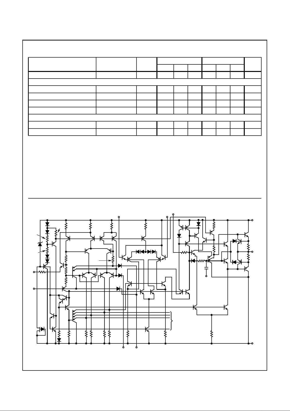
Schematic Diagram
HA-2400
Settling Time (Notes 4, 5, 9) V
OUT
= 10V
P-P
25 - 1.5 2.5 - 1.5 2.5 µs
CHANNEL SELECT CHARACTERISTICS
Digital Input Current VIN = 0V Full - 1 1.5 - 1 1.5 mA
Digital Input Current VIN = +5.0V Full - 5 - - 5 - nA
Output Delay (Notes 6, 9) 25 - 100 250 - 100 250 ns
Crosstalk (Note 7) 25 -80 -110 - -74 -110 - dB
POWER SUPPLY CHARACTERISTICS
Supply Current 25 - 4.8 6.0 - 4.8 6.0 mA
Power Supply Rejection Ratio VS = ±10V to ±20V Full 74 90 - 74 90 - dB
NOTES:
3. AV = +10, C
COMP
= 0, RL = 2kΩ, CL = 50pF.
4. AV = +1, C
COMP
= 15pF, RL = 2kΩ, CL = 50pF.
5. To 0.1% of final value.
6. To 10% of final value; output then slews at normal rate to final value.
7. Unselected input to output; VIN = ±10VDC.
8. Unselected channels have approximately the same input parameters.
9. Guaranteed by design.
10. Full Power Bandwidth based on slew rate measurement using: .
11. See Figure 13 for test circuit.
Electrical Specifications Test Conditions: V
SUPPLY
= ±15V, Unless Otherwise Specified. Digital Inputs: VIL = +0.5V, VIH = +2.4.
Limits apply to each of the four channels, when addressed (Continued)
PARAMETER
TEST
CONDITIONS
TEMP.
(oC)
HA-2400/04 HA-2405
UNITSMIN TYP MAX MIN TYP MAX
FPBW
SR
2πV
PEAK
-------------------------- -
V
PEAK
; 5V==
ENABLE
GND
OUT
R
2
2.4K
R
4
22.9K
Q
1
Q
3
Q
4
Q
6
Q
7
Q
8
R
1
1.6K
R
3
1.8K
Q
2
Q
5
R
5
8.0K
R
6
2.0K
R
35
1.6K R
7
5.6K
Q
10
Q
11
Q
13
Q
12
Q
15
Q
14
R
8
4K
Q
16
R
9
1.5K
R
10
10K
R
11
10K
VA
VC
Q17
VB
Q
18
Q
19
Q
20
VD
R
12
1.6K
Q
28
VE
R
13
0.8K
Q
22
R
15
10K
R
16
10K
Q
21
Q
26
Q
27
R
14
10K
Q
29
Q
23
Q
24
Q
25
Q
30
Q
32
Q
33
Q
102
Q
34
Q
38
R
18
2.0K
Q
103
Q
35
Q
31
Q
36
Q
37
Q
39
Q
40
Q
41
Q
79
Q
81
Q
82
Q
84
Q
80
Q
83
Q
86
Q
89
Q
88
R
35
0.75K
Q
85
Q
98
Q
92
R
30
1.2K
C
1
9.0pF
V+
Q
93
Q
42
R19
1.6K
TO ADDITIONAL
INPUT STAGES
R
29
0.4K
Q
90
Q
91
R
33
4K
Q
97
Q
100
Q
99
Q
95
Q
94
+V
CC
-V
EE
R
31
36.5
R
32
34
Q
96
COMPIN-IN+
D1D0
R
17
1.6K
Q
87
R
34
1.6K
Q
101
Q
9
Diagram Includes: One Input Stage, Decode Control, Bias Network, and Output Stage
HA-2400, HA-2404, HA-2405
Page 4

3-164
Typical Applications
FIGURE 1. HA-2400 AMPLIFIER, NONINVERTING
PROGRAMMABLE GAIN
FIGURE 2. HA-2400 SAMPLE AND HOLD
For more examples, see Intersil Application Note AN514.
+
2
1K
500
500
ENABLE
GND
COMP
OUTPUT
AMP
V-
13
8
1
2
3
4
5
7
6
V+
+
4
+
3
+
1
14
15
16
12
11
10
9
+
D1
D0
15pF
IN
2K
-15V
DECODE/
CONTROL
DIGITAL
DIGITAL
GROUND
CONTROL
+15V
OUT
1
ENABLE
GND
COMP
OUTPUT
AMP
V-
13
8
1
2
3
4
5
7
6
V+
+
4
+
3
+
+
2
14
15
16
12
11
10
9
D1
D0
-15V
DIGITAL
GROUND
+15V
C
OUT
S
H
IN
DECODE/
CONTROL
I1≈ 150 x 10-6A
I2≈ 200 x 10-9A at 25oC
≈ 600 x 10-9A at -55oC
≈ 100 x 10-9A at 125oC
Q ≈ 2 x 10
-12
C
Sample Charging Rate
I
1
C
---- -
Vs⁄=
Hold Drift Rate
I
2
C
---- -
Vs⁄=
Switch Pedestal Error
Q
C
----
V=
-
-
-
HA-2400, HA-2404, HA-2405
Page 5

3-165
Typical Performance Curves
FIGURE 3. INPUT BIAS CURRENT AND OFFSET CURRENT vs
TEMPERATURE
FIGURE 4. NORMALIZED AC PARAMETERS vs TEMPERATURE
FIGURE 5. POWER SUPPLY CURRENT vs TEMPERATURE
FIGURE 6. OPEN LOOP FREQUENCY AND PHASE RESPONSE
FIGURE 7. FREQUENCY RESPONSE vs C
COMP
FIGURE 8. NORMALIZED AC PARAMETERS vs SUPPLY
VOLTAGE
TEMPERATURE (oC)
-55 -50 -25 0 25 50 75 100 125
CURRENT (nA)
0
5
10
40
60
80
100
120
140
BIAS CURRENT
OFFSET CURRENT
TEMPERATURE (oC)
-55 -50 -25 0 25 50 75 100 125
NORMALIZED VALUE REFERRED TO 25
o
C
0.8
0.9
1.0
1.1
1.2
BANDWIDTH
SLEW RATE
TEMPERATURE (oC)
-55 -50 -25 0 25 50 75 100 125
SUPPLY CURRENT (mA)
3
4
5
V
SUPPLY
= ±20V
V
SUPPLY
= ±15V
V
SUPPLY
= ±10V
CROSST ALK REJECTION, AV = +1
C
COMP
= 0pF
PHASE
C
COMP
= 15pF
GAIN
OPEN LOOP VOLTAGE GAIN (dB)
-20
0
20
40
60
80
100
120
FREQUENCY (Hz)
10 100 1K 10K 100K 1M 10M 100M
0
30
60
90
120
150
180
210
PHASE (DEGREES)
FREQUENCY (Hz)
10 100 1K 10K 100K 1M 10M 100M
OPEN LOOP VOLTAGE GAIN (dB)
-20
0
20
40
60
80
100
120
1000pF
300pF
100pF
30pF
15pF
0pF
SLEW RATE
BANDWIDTH
SUPPLY VOLTAGE (V)
±10 ±20±15
0.8
0.9
1.0
1.1
1.2
NORMALIZED VALUE REFERRED TO ±15V
HA-2400, HA-2404, HA-2405
Page 6

3-166
FIGURE 9. OPEN LOOP VOLTAGE GAIN vs TEMPERATURE FIGURE 10. OUTPUT VOLTAGE SWING vs FREQUENCY
FIGURE 11. EQUIVALENT INPUT NOISE vs BANDWIDTH FIGURE 12. INPUT NOISE vs FREQUENCY
FIGURE 13. SLEW RATE AND TRANSIENT RESPONSE
Typical Performance Curves (Continued)
TEMPERATURE (oC)
-55 -50 -25 0 25 50 75 100 125
GAIN (dB)
90
100
110
V
SUPPLY
= ±20V
V
SUPPLY
= ±15V
V
SUPPLY
= ±10V
105
95
FREQUENCY (Hz)
10K 100K 1M 10M
OUTPUT SWING (V
P-P
)
0.1
1.0
10
20
C
COMP
= 0pF
C
COMP
= 15pF
100Hz 1kHz 10kHz 100kHz 1MHz
UPPER 3dB FREQUENCY (LOWER 3dB FREQUENCY-10Hz)
BROADBAND NOISE CHARACTERISTICS
INPUT NOISE (µV)
100
10
1.0
0.1
0 SOURCE RESISTANCE
10K SOURCE RESISTANCE
THERMAL NOISE OF 10K RESISTOR
1 100 1K 10K 100K10
FREQUENCY (Hz)
INPUT NOISE CURRENT (pA/√Hz)
INPUT NOISE VOLTAGE (nV/√
Hz)
1000
100
10
1
10
1
0.1
0.01
INPUT NOISE VOLTAGE
INPUT NOISE CURRENT
COMP
AV = 1
IN
15pF
+15.0V
OUT
SELECTED
CHANNEL
-15.0V
1800Ω
200Ω
+
-
AV = 10
50pF
45Ω
5Ω
HA-2400, HA-2404, HA-2405
Page 7

3-167
All Intersil semiconductor products are manufactured, assembled and tested under ISO9000 quality systems certification.
Intersil products are sold by description only. Intersil Corporation reserves the right to make changes in circuit design and/or specifications at any time without
notice. Accordingly, the reader is cautioned to verify that data sheets are current before placing orders. Information furnished by Intersil is believed to be accurate
and reliable. However, no responsibility is assumed by Intersil or its subsidiaries f or its use; nor for any infringements of patents or other rights of third parties which
may result from its use. No license is granted by implication or otherwise under an y patent or patent rights of Intersil or its subsidiaries.
For information regarding Intersil Corporation and its products, see web site http://www.intersil.com
Sales Office Headquarters
NORTH AMERICA
Intersil Corporation
P. O. Box 883, Mail Stop 53-204
Melbourne, FL 32902
TEL: (321) 724-7000
FAX: (321) 724-7240
EUROPE
Intersil SA
Mercure Center
100, Rue de la Fusee
1130 Brussels, Belgium
TEL: (32) 2.724.2111
FAX: (32) 2.724.22.05
ASIA
Intersil (Taiwan) Ltd.
Taiwan Limited
7F-6, No. 101 Fu Hsing North Road
Taipei, Taiwan
Republic of China
TEL: (886) 2 2716 9310
FAX: (886) 2 2715 3029
HA-2400, HA-2404, HA-2405
 Loading...