

Page 1
HA22033
GaAs MMIC
Low Noise Amplifier for Micro Wave Application
Features
• Suitable for low noise amplifier of Micro Wave Application(1.5 to 1.9GHz)
• Low voltage and low current operation (2.7V, 1.7mA typ.)
• Low noise (1.4 dB typ. @1.5GHz)
• High power gain (14 dB typ. @1.5GHz)
• Built–in matching circuits (50Ω)
• Small surface mount package (MPAK–5)
ADE-207-266 (Z)
1st. Edition
October 1998
Outline
MPAK–5
This document may, wholly or partially, be subject to change without notice.
This Device si sensitive to Electro Static Discharge.
An Adequate handling procedure is requested.
CAUTION
This product ues GaAs. Since dust or fume of GaAs is highly poisonous to human body, please do not
Page 2

HA22033
Absolute Maximum Ratings (Ta = 25°C)
Item Symbol Ratings Unit
Supply voltage Vdd 5 V
Maximum current Idd 6 mA
Power dissipation Pd 100 mW
Channel temperature Tch 150 °C
Storage temperature Tstg –55 to +125 °C
Operation temperature Topr –20 to +70 °C
Maximum input power Pin max +15 dBm
Electrical Characteristics (Ta = 25°C, Vdd = 2.7V)
Item Symbol Min Typ Max Unit Test Conditions Pin
Quiescent current Idd — 1.7 2.5 mA No signal
Power gain PG 12 14 — dB f = 1.5 GHz
Noise figure NF — 1.4 2 dB f = 1.5 GHz
Typical Performance (Ta = 25°C, Vdd = 2.7V)
Item Symbol Typ Unit Test Conditions Pin
VSWR (input) VSWR in 1.5 — f = 1.5 GHz 4
VSWR (output) VSWR out 2.2 — f = 1.5 GHz 1
3rd order intermodulation
distortion
IM3 50 dB f = 1.5 GHz, Pin = –30 dBm
Page 3
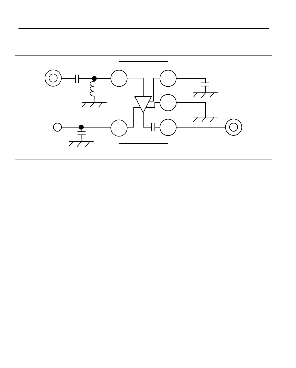
Block Diagram
HA22033
in
Vdd
1.5pF
5.6nH
100pF
4
5
3
2
1
Cs
100pF
GND
out
Page 4
HA22033
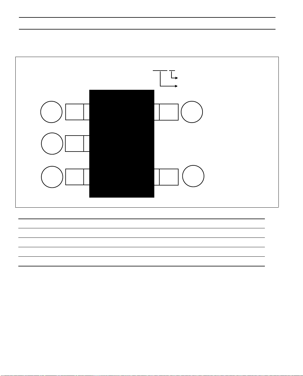
Pin Arrangement
G E A
Monthly code (variable)
Mark type
1
GEA
5
2
3
Top View
Pin No. Pin name Function
1 RF out RF output
2 GND Ground
3 Cs Bypath capacitor (>100 pF)
4 RF in RF input
5 Vdd Power supply
4
Page 5

Pattern Layout
HA22033
scale 4/1
: φ0.5mm
: φ0.3mm
RF in
Front Side view of PCB Pattern
100pF
5.6nH
1.5pF
Vdd
Front Side view of Part Layout(1.5GHz)
cs
GEA
100pF
scale 4/1
: Capacitor
: Inductor
RF out
ER=4.8
H=1mm
Page 6

HA22033
Main Characteristics
20
15
10
5
Power Gain PG (dB)
0
1.0 1.5 2.0 2.5
6
5
Power Gain vs. Frequency Noise Figure vs. Frequency
Vdd = 2.7 V
Ta = +25°C
Frequency f (GHz)
VSWR vs. Frequency
Vdd = 2.7 V
Ta = +25°C
4
3
2
1
Noise Figure NF (dB)
Vdd = 2.7 V
Ta = +25°C
0
1.0 1.5 2.0 2.5
Frequency f (GHz)
Output Power, 3rd Order Inter–
modlation Distortion vs. Input Power
20
Vdd = 2.7 V
f = 1.5 GHz
ud = 1.5006 GHz
0
Ta = +25°C
4
VSWR
3
2
1
1.0 1.5 2.0 2.5
Frequency f (GHz)
output
input
–20
–40
–60
Output Power Pout (dBm)
–80
–60 –50
Input Power Pin (dBm)
Pout
–30 –20 –10 0 10
–40
im3
Page 7

HA22033
Power Gain vs. Supply Voltage
20
f = 1.5 GHz
Ta = +25°C
15
10
5
Power Gain PG (dB)
0
2.5 3 3.5 4 4.5
2
Supply Voltage Vdd (V)
5
4
3
VSWR
VSWR vs. Supply Voltage
f = 1.5 GHz
Ta = +25°C
Noise Figure vs. Supply Voltage
4
f = 1.5 GHz
Ta = +25°C
3
2
1
Noise Figure NF (dB)
0
5
2 3 3.5 4 4.5 5
2.5
Supply Voltage Vdd (V)
Pout @ 1dB Gain Compression, 3rd Order
Inter–cept Point (out) vs. Supply Voltage
20
f = 1.5 GHz
ud = 1.5006 GHz
Ta = +25°C
15
10
5
IP3o
2
1
2.5 3 3.5 4 4.5
2
Supply Voltage Vdd (V)
output
input
P1dB, IP3o (dBm)
0
–5
5
2 3 3.5 4 4.5 5
P1dB
2.5
Supply Voltage Vdd (V)
Page 8

HA22033
20
15
10
Power Gain PG (dB)
Power Gain vs. Temperature
Vdd =2.7 V
f = 1.5 GHz
5
0
–250255075
Ambient Temperature Ta (°C)
VSWR vs. Temperature
5
Vdd = 2.7 V
f = 1.5 GHz
4
Noise Figure vs. Temperature
4
Vdd = 2.7 V
f = 1.5 GHz
3
2
1
Noise Figure NF (dB)
0
–250255075
Ambient Temperature Ta (°C)
Pout @ 1dB Gain Compression, 3rd Order
Inter–cept Point (out) vs. Ambient Temperature
20
Vdd = 2.7 V
f = 1.5 GHz
ud = 1.5006 GHz
15
3
VSWR
output
2
input
1
–250255075
Ambient Temperature Ta (°C)
10
5
P1dB, IP3o (dBm)
0
–5
–250255075
Ambient Temperature Ta (°C)
P1dB
IP3o
Page 9

HA22033
Quiescent Current vs. Supply Voltage
5
Ta = +25°C
4
3
2
1
Quiescent Current Idd (mA)
0
2 3 3.5 4 4.5 5
2.5
Supply Voltage Vdd (V)
Quiescent Current vs.
Ambient Temperature
5
Vdd = 2.7 V
4
3
2
1
Quiescent Current Idd (mA)
0
–250255075
Ambient Temperature Ta (°C)
Page 10

HA22033
Package Dimentions
2.9 ± 0.2
0.95 0.95
0.4 ± 0.1
1.9
0.3
+ 0.2
0.4 ± 0.1
– 0.1
1.1
0.6
0.16
+ 0.1
– 0.06
Unit: mm
0.4 ± 0.1
+ 0.2
1.6
– 0.1
0.6
+ 0.2
2.8
– 0.3
0 to 0.1
Hitachi code
EIAJ
JEDEC
MPAK–5
—
—
Page 11

HA22033
Cautions
1. Hitachi neither warrants nor grants licenses of any rights of Hitachi’s or any third party’s patent,
copyright, trademark, or other intellectual property rights for information contained in this document.
Hitachi bears no responsibility for problems that may arise with third party’s rights, including
intellectual property rights, in connection with use of the information contained in this document.
2. Products and product specifications may be subject to change without notice. Confirm that you have
received the latest product standards or specifications before final design, purchase or use.
3. Hitachi makes every attempt to ensure that its products are of high quality and reliability. However,
contact Hitachi’s sales office before using the product in an application that demands especially high
quality and reliability or where its failure or malfunction may directly threaten human life or cause risk
of bodily injury, such as aerospace, aeronautics, nuclear power, combustion control, transportation,
traffic, safety equipment or medical equipment for life support.
4. Design your application so that the product is used within the ranges guaranteed by Hitachi particularly
for maximum rating, operating supply voltage range, heat radiation characteristics, installation
conditions and other characteristics. Hitachi bears no responsibility for failure or damage when used
beyond the guaranteed ranges. Even within the guaranteed ranges, consider normally foreseeable
failure rates or failure modes in semiconductor devices and employ systemic measures such as failsafes, so that the equipment incorporating Hitachi product does not cause bodily injury, fire or other
consequential damage due to operation of the Hitachi product.
5. This product is not designed to be radiation resistant.
6. No one is permitted to reproduce or duplicate, in any form, the whole or part of this document without
written approval from Hitachi.
7. Contact Hitachi’s sales office for any questions regarding this document or Hitachi semiconductor
products.
1. This product must not be placed in the mouth, as it contains toxic substances that may cause poisoning.
If by chance the product is placed in the mouth, take emergency action such as inducing vomiting, then
consult a physician without delay.
2. Disposal of this product must be handled, separately from other general refuse, by a specialist
processing contractor in the same way as dangerous items.
Page 12

HA22033
Hitachi, Ltd.
Semiconductor & IC Div.
Nippon Bldg., 2-6-2, Ohte-machi, Chiyoda-ku, Tokyo 100-0004, Japan
Tel: Tokyo (03) 3270-2111 Fax: (03) 3270-5109
URL NorthAmerica : http:semiconductor.hitachi.com/
For further information write to:
Hitachi Semiconductor
(America) Inc.
2000 Sierra Point Parkway
Brisbane, CA 94005-1897
Tel: <1> (800) 285-1601
Fax: <1> (303) 297-0447
Europe : http://www.hitachi-eu.com/hel/ecg
Asia (Singapore) : http://www.has.hitachi.com.sg/grp3/sicd/index.htm
Asia (Taiwan) : http://www.hitachi.com.tw/E/Product/SICD_Frame.htm
Asia (HongKong) : http://www.hitachi.com.hk/eng/bo/grp3/index.htm
Japan : http://www.hitachi.co.jp/Sicd/indx.htm
Hitachi Europe GmbH
Electronic components Group
Dornacher Straße 3
D-85622 Feldkirchen, Munich
Germany
Tel: <49> (89) 9 9180-0
Fax: <49> (89) 9 29 30 00
Hitachi Europe Ltd.
Electronic Components Group.
Whitebrook Park
Lower Cookham Road
Maidenhead
Berkshire SL6 8YA, United Kingdom
Tel: <44> (1628) 585000
Fax: <44> (1628) 778322
Hitachi Asia Pte. Ltd.
16 Collyer Quay #20-00
Hitachi Tower
Singapore 049318
Tel: 535-2100
Fax: 535-1533
Hitachi Asia Ltd.
Taipei Branch Office
3F, Hung Kuo Building. No.167,
Tun-Hwa North Road, Taipei (105)
Tel: <886> (2) 2718-3666
Fax: <886> (2) 2718-8180
Copyright © Hitachi, Ltd., 1998. All rights reserved. Printed in Japan.
Hitachi Asia (Hong Kong) Ltd.
Group III (Electronic Components)
7/F., North Tower, World Finance Centre,
Harbour City, Canton Road, Tsim Sha Tsui,
Kowloon, Hong Kong
Tel: <852> (2) 735 9218
Fax: <852> (2) 730 0281
Telex: 40815 HITEC HX
 Loading...