

Page 1

HA1835P/HA1848P
Watchdog Timer
Description
The HA1835P and HA1848P is a monolithic voltage regulator control designed for microcomputer
systems. In addition to the voltage regulator, it include watchdog timer function and power-on reset
function.
These ICs can perform many function in various microcomputer systems with few external parts.
Features
• Regulated power supply control function
Wide area of operational voltage; VCC = 6 V to 30 V
Available external PNP-type transistor, suited to any system power supply
Built-in overcurrent limiter for external PNP-type transistor
Output voltage can be adjusted exactry in the range from 4 V to 6 V
• Watchdog timer
Internal bandpass filter control circuit (pulse width detect type) and reset signal oscillator
Fail-safe utility
Bandpass filter characteristics can be set by external resister (Rf) and capacitance (Cf)
• Automatic reset
Automatic power-on reset
Pulse generator characteristics can be set by external resistor (RR) and capacitance (CR)
Alternative between RES and RES output
Page 2
HA1835P/HA1848P
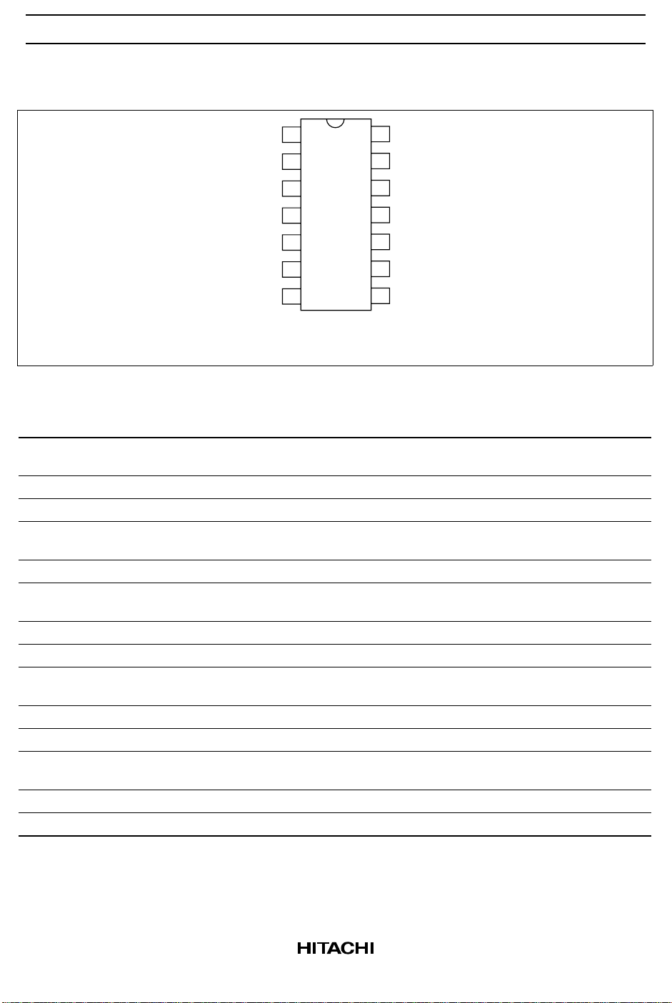
Pin Arrangement
R
C
P-RUN
Rf
Cf
Vout
GND
1
R
2
R
3
4
5
6
7
14
13
12
11
10
RES
RES
CS
V
CC
V
CONT
Comp *
9
Vadj
8
(Top View)
Note: HA1848P: 9 pin is non connection.
Pin Functions
Pin No. Symbol Functions
1R
2C
R
R
3 P-RUN Clock pulse input terminal for watchdog timer
4 Rf Frequency band width of filter circuit depends on resistance connected to Rf
5 Cf Frequency band width of filter circuit depends on capacitance connected to Cf
6 Vout Connect to external PNP transistor's collector: This pin supplies 5 V regulated
7 GND Ground
8 Vadj Output voltage fine tuning terminal
9 Comp Phase compensation terminal: Connect less than 100 pF capacitor between V
10 V
11 V
CONT
CC
12 CS Connect current sense resistor, which protects the external PNP transistor,
13 RES * Reset pulse output terminal for low level reset type microcomputer
14 RES * Reset pulse output terminal for high level reset type microcomputer
Note: RES and RES are open-collector output terminals, so connect a pull-up resistor of about 5 kΩ.
Reset pulse width depends on resistance connected to R
R
Recommended range: 100 kΩ to 1 MΩ
Reset pulse width depends on capacitance connected to C
R
Recommended range: 100 kΩ to 500 kΩ
voltage for internal circuit
and Comp. HA1848P is non connection
External PNP transistor's base control terminal
Supply voltage terminal: Operating supply voltage range is 6 V to 30 V
between V
and CS
CC
CC
2
Page 3
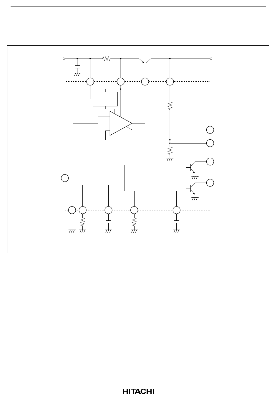
Block Diagram
V
CC
C
1
Reference
Voltage
11
R
V
CC
Current
Limiter
CS
12
Error
Amp
CS
Q
10
V
CONT
HA1835P/HA1848P
Vout
Vout HA1835P
6
5 kΩ
2 kΩ
9 Comp *
8 Vadj
14 RES
Fail Detector
3P-RUN
(Band Pass Filter)
4 5
Rf
300 kΩCf0.01 µF
Power on Reset Detector
Reset Signal Oscillator
1 27
R
R
560 kΩ
GND
Note: HA1848P: 9 pin is non connection.
C
R
0.1 µF
13 RES
3
Page 4

HA1835P/HA1848P
Absolute Maximum Ratings (Ta = 25°C)
Item Symbol Rating Unit
Supply voltage V
P-RUN input voltage V
Output voltage V
Output current I
Control terminal voltage V
Control terminal current I
CC
P-RUN
RES
V
RES
RES
I
RES
CONT
CONT
Power dissipation (Note) PT * 400 mW
Operating temperature range Topr –40 to +85 °C
Storage temperature range Tstg –50 to +125 °C
Soldering temperature Tsol +260 (< 10 sec) °C
Note: Ta ≤ 77°C. If Ta > 77°C, derate by 8.3 mW/°C.
30 V
–0.3 to Vout V
17.5 V
17.5 V
2mA
2mA
V
CC
V
20 mA
4
Page 5
HA1835P/HA1848P
Electrical Characteristics (VCC = 12 V, Vout = 5 V, Ta = 25°C)
Item Symbol Min Typ Max Unit Test Conditions
Power supply terminal current I
CC
Regulator Output voltage Vout1 4.75 5.00 5.25 V VCC = 6 to 17.5 V, Iout = 0.5 A
section Vout2 4.70 5.00 5.30 V VCC = 6 to 17.5 V, Iout = 1 A
Line regulation δV
Load regulation δV
Ripple rejection R
Limiter operating current I
Output voltage temperature
Oline
Oload
REJ
CS
δVout/δT — –0.6 — mV/°C
coefficient
P-RUN input Low-level input voltage V
section High-level input voltage V
Low-level input current I
High-level input current I
Reset circuit
section
Reset terminal low-level
voltage
Reset terminal I
leakage current I
Reset time Power on time t
Clock off reset time t
Reset pulse low-level time t
Reset pulse high-level time t
V
IL
IH
IL
IH
OL1
OH1
OH3
on
off
RL
RH
— 6.3 12 mA VCC = 17.5 V (No load),
with PNP transistor
–50 — +50 mV VCC = 6 to 17.5 V, Iout = 1 A
–100 — +100 mV Iout = 10 mA to 0.5 A
40 75 — dB ei = 0.5 Vrms, fi = 1 kHz
1.0 — 2.0 A RSC = 0.2 Ω
— — 0.8 V
2.0 — — V
–120 –60 — µAVIL = 0 V
— 1.8 3.0 mA Vout = 5 V, VIH = 5 V
— — 0.4 V IOL = 2 mA
— — 5.0 µAVOH = 5 V
——30µAVOH = 17.5 V
80 130 200 ms Rf = 300 kΩ, RR = 560 kΩ,
60 130 220 ms Cf = 0.01 µF, CR = 0.1 µF
40 80 160 ms
50 100 200 ms
5
Page 6

HA1835P/HA1848P
Test Circuit
S
12 CS Vout
0.2 Ω
R
SC
11 V
S
1
V
Batt
Rf
2
CC
4
3
P-RUN
Cf
5
2SB857D
10
V
CONT
HA1835P
GND
7
+
C
5 kΩ
5 kΩ
−
100 µF
2
RES 14
13
RES
Vadj68
R
R
1
C
R
2
Counter
300 kΩ
0.01 µF
560 kΩ
0.1 µF
6
Page 7

HA1835P/HA1848P
Functional Description
Voltage Regulator
The HA1835P, and HA1848P supplies 5 V regulated output from a wide VCC input range (VCC = 6 V to
17.5 V). The external PNP transistor should be selected according to the supply current demand of the
system. Connect a more than 100 µF capacitor between Vout and GND to realize the 5 V regulated output.
The resistor connected from the Vadj terminal to the Vout or GND terminal fine tunes the output voltage.
A resistor between Vadj and the Vout decreases the output voltage, and a resistor between Vadj and GND
increases the output voltage.
R (Vout − Vadj) ≈ (kΩ)
R (Vadj − GND) ≈ (kΩ)
5 ⋅ Vout − 7.14
5 − Vout
7.14
Vout − 5
Current Limiter
To protect the external transistor from overcurrent, connect a current-sense resistor between the CS
terminal and the VCC terminal. The value of this resistor should be:
R
SC
0.3 V
≈ (at Ta = 25°C)
Iout (Limit)
Power-On Reset
The HA1835P, and HA1848P can output a reset pulse to start the microcomputer at power on (figure 6).
The external resistor RR and capacitor CR determine the power-on reset timing.
Note that RES and RES are open-collector terminals. They should therefore be connected to a pull-up
resistor of about 5 kΩ.
Watchdog Timer
The watchdog timer is a fail-safe function. It can reset the microcomputer system if the system runs out of
control. It does this be monitoring a pulse output by the system's software. It uses a bandpass filter to
determine whether the pulse frequency is within the system's normal frequency band (figure 7, 8). External
resistor and capacitor Rf and Cf determine the frequency range of the bandpass filter. If the pulse
frequency is not within the frequency band, the HA1835P, and HA1848P outputs a reset pulse.
7
Page 8

HA1835P/HA1848P
Application Circuit Example
R
V
CC
SC
0.2 Ω
1211
CS
V
Batt
+
C
1
−
10 µF
Q
2SB857D
10
V
CONT
6
Vout
5 kΩ
13
RES RES
V
C
2
100 µF
Reg
+
−
V
CC
Microcomputer
system
Rf
4
Rf
300 kΩ
Cf
5
Cf
0.01 µF
GND
7
R
R
1
P-RUN
R
R
560 kΩ
C
2
3
R
C
R
0.1 µF
I/O port
System burst
V
CC
P-RUN
RES
t
on
Power-on reset signal
t
RL
t
off
t
RH
Reset output signal 3 Hz
8
Page 9

Characteristic Curves
HA1835P/HA1848P
5
4
(V)
OUT
V
3
I
= 0.1 A
2
Output voltage
1
0
0510
OUT
0.5 A
1.0 A
Input voltage
Figure 1 Output Voltage vs. Input Voltage
6
(V)
OUT
4
V
Ta = 25°C
VIN (V)
Ta = 25°C
Ω
2
R = 0.5
0.2 Ω
Output voltage
0
012
Output current
I
(A)
OUT
Figure 2 Output Voltage vs. Output Current
5.1
(V)
OUT
V
5.0
VIN = 12 V
= 1 A
I
OUT
Output voltage
4.9
−50 500 100
Ambient temperature
Ta (°C)
Figure 3 Output Voltage vs. Ambient Temperature
9
Page 10

HA1835P/HA1848P
200
(ms)
100
RH
t
0
Automatic reset pulse high time
200
(ms)
100
RL
t
VIN = 12 V
Ta = 25°C
= 0.22 µF
R
C
C
200 k 500 k
Resistor R
R
(Ω)
Figure 4 Automatic Reset Pulse High Time vs. Resistor
V
= 12 V
IN
Ta = 25°C
C
= 0.1 µF
R
C
= 0.047 µF
R
= 0.22 µF
R
1 M50 k 100 k
0
Automatic reset pulse low time
Figure 5 Automatic Reset Pulse Low Time vs. Resistor
100
(ms)
on
VIN = 12 V
Ta = 25°C
50
0
Power-on reset time t
Figure 6 Power-on Reset Time vs. Resistor
Resistor RR (Ω)
= 0.22 µF
R
C
Resistor R
R
(Ω)
= 0.1 µF
C
R
= 0.047 µF
C
R
= 0.1 µF
R
C
= 0.047 µF
R
C
1 M50 k 100 k 200 k 500 k
1 M50 k 100 k 200 k 500 k
10
Page 11

HA1835P/HA1848P
5 k
Ta = 25°C
V
= 12 V
IN
2 k
1 k
500
Allowable operation
clock pulse duty
200
Clock pulse frequency f (Hz)
100
50
30
0 20 40 60 80 100
Clock pulse duty cycle (%)
Figure 7 Clock Pulse Frequency vs. Clock Pulse Duty Cycle
cycle
Duty =
AB
B
A + B
Ta = 25°C
20 k
V
= 12 V
IN
Duty = 50%
10 k
5 k
2 k
1 k
500
System run-away
sense region
Normal operation region
200
Clock pulse frequency f (Hz)
100
50
System run-away
sense region
20
100 k 200 k 500 k
Resistor Rf (Ω)
Figure 8 Clock Pulse Frequency vs. Resistor
11
Page 12
HA1835P/HA1848P
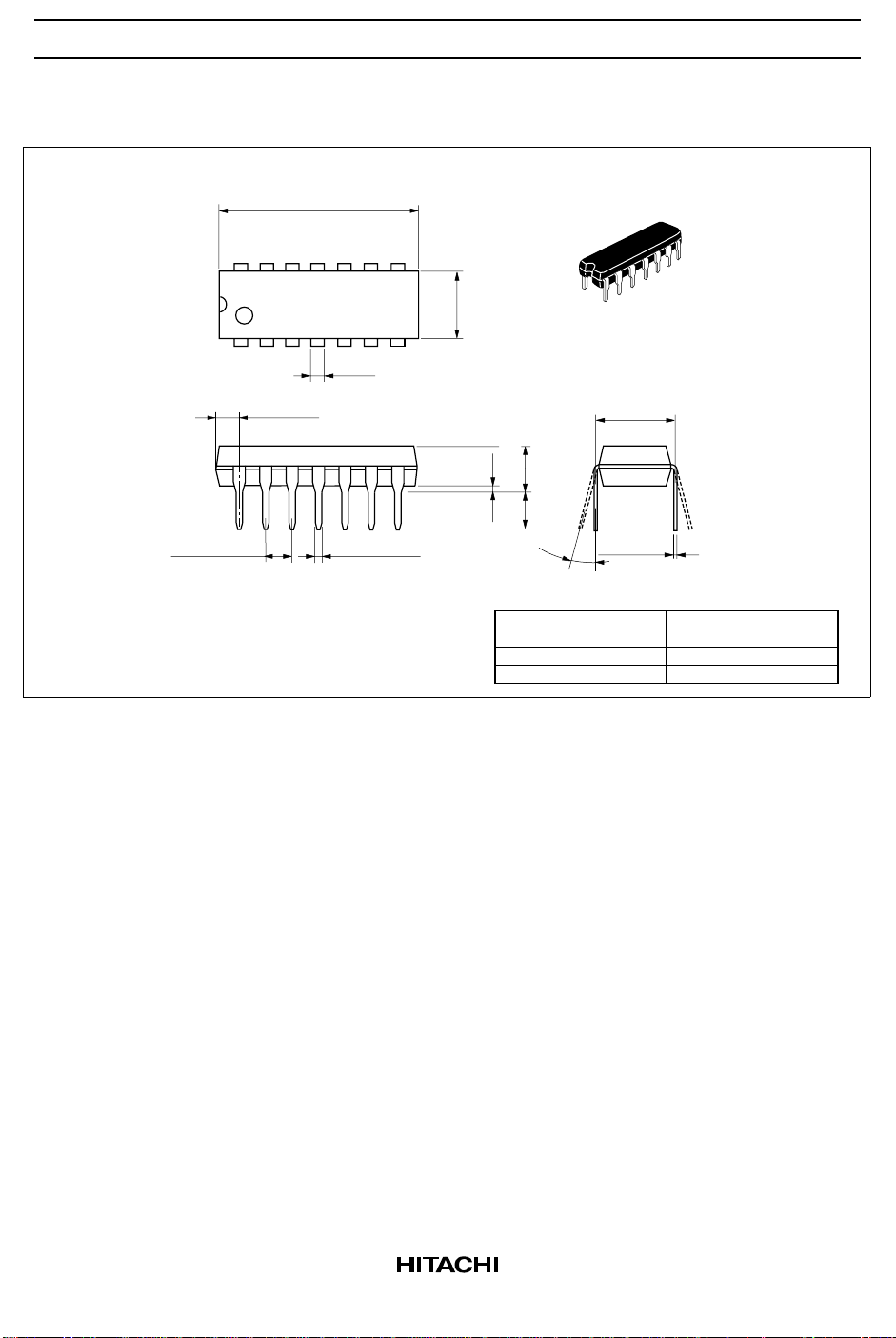
Package Dimensions
1
19.20
20.32 Max
1.30
Unit: mm
814
6.30
7.40 Max
7
2.54 ± 0.25
2.39 Max
0.48 ± 0.10
2.54 Min 5.06 Max
0.51 Min
Hitachi Code
JEDEC
EIAJ
Mass
7.62
+ 0.10
0.25
– 0.05
0° – 15°
(reference value)
DP-14
Conforms
Conforms
0.97 g
12
Page 13

HA1835P/HA1848P
Cautions
1. Hitachi neither warrants nor grants licenses of any rights of Hitachi’s or any third party’s patent,
copyright, trademark, or other intellectual property rights for information contained in this document.
Hitachi bears no responsibility for problems that may arise with third party’s rights, including
intellectual property rights, in connection with use of the information contained in this document.
2. Products and product specifications may be subject to change without notice. Confirm that you have
received the latest product standards or specifications before final design, purchase or use.
3. Hitachi makes every attempt to ensure that its products are of high quality and reliability. However,
contact Hitachi’s sales office before using the product in an application that demands especially high
quality and reliability or where its failure or malfunction may directly threaten human life or cause risk
of bodily injury, such as aerospace, aeronautics, nuclear power, combustion control, transportation,
traffic, safety equipment or medical equipment for life support.
4. Design your application so that the product is used within the ranges guaranteed by Hitachi particularly
for maximum rating, operating supply voltage range, heat radiation characteristics, installation
conditions and other characteristics. Hitachi bears no responsibility for failure or damage when used
beyond the guaranteed ranges. Even within the guaranteed ranges, consider normally foreseeable
failure rates or failure modes in semiconductor devices and employ systemic measures such as failsafes, so that the equipment incorporating Hitachi product does not cause bodily injury, fire or other
consequential damage due to operation of the Hitachi product.
5. This product is not designed to be radiation resistant.
6. No one is permitted to reproduce or duplicate, in any form, the whole or part of this document without
written approval from Hitachi.
7. Contact Hitachi’s sales office for any questions regarding this document or Hitachi semiconductor
products.
Hitachi, Ltd.
Semiconductor & Integrated Circuits.
Nippon Bldg., 2-6-2, Ohte-machi, Chiyoda-ku, Tokyo 100-0004, Japan
Tel: Tokyo (03) 3270-2111 Fax: (03) 3270-5109
URL NorthAmerica : http:semiconductor.hitachi.com/
For further information write to:
Hitachi Semiconductor
(America) Inc.
179 East Tasman Drive,
San Jose,CA 95134
Tel: <1> (408) 433-1990
Fax: <1>(408) 433-0223
Europe : http://www.hitachi-eu.com/hel/ecg
Asia (Singapore) : http://www.has.hitachi.com.sg/grp3/sicd/index.htm
Asia (Taiwan) : http://www.hitachi.com.tw/E/Product/SICD_Frame.htm
Asia (HongKong) : http://www.hitachi.com.hk/eng/bo/grp3/index.htm
Japan : http://www.hitachi.co.jp/Sicd/indx.htm
Hitachi Europe GmbH
Electronic components Group
Dornacher Straβe 3
D-85622 Feldkirchen, Munich
Germany
Tel: <49> (89) 9 9180-0
Fax: <49> (89) 9 29 30 00
Hitachi Europe Ltd.
Electronic Components Group.
Whitebrook Park
Lower Cookham Road
Maidenhead
Berkshire SL6 8YA, United Kingdom
Tel: <44> (1628) 585000
Fax: <44> (1628) 778322
Hitachi Asia Pte. Ltd.
16 Collyer Quay #20-00
Hitachi Tower
Singapore 049318
Tel: 535-2100
Fax: 535-1533
Hitachi Asia Ltd.
Taipei Branch Office
3F, Hung Kuo Building. No.167,
Tun-Hwa North Road, Taipei (105)
Tel: <886> (2) 2718-3666
Fax: <886> (2) 2718-8180
Copyright ' Hitachi, Ltd., 1998. All rights reserved. Printed in Japan.
Hitachi Asia (Hong Kong) Ltd.
Group III (Electronic Components)
7/F., North Tower, World Finance Centre,
Harbour City, Canton Road, Tsim Sha Tsui,
Kowloon, Hong Kong
Tel: <852> (2) 735 9218
Fax: <852> (2) 730 0281
Telex: 40815 HITEC HX
13
 Loading...