

Page 1
HA17902 Series
Quad Operational Amplifier
Description
The HA17902 is an internal phase compensation quad operational amplifier that operates on a singlevoltage power supply and is appropriate for use in a wide range of general-purpose control equipment.
Features
• Wide usable power-supply voltage range and single-voltage supply operation
• Internal phase compensation
• Wide common-mode voltage range and operation for inputs close to the 0 level
Ordering Information
Type No. Application Package
HA17902PJ Car use DP-14
HA17902FPJ FP-14DA
HA17902FPK FP-14DA
HA17902P Industrial use DP-14
HA17902FP FP-14DA
HA17902 Commercial use DP-14
Page 2
HA17902 Series
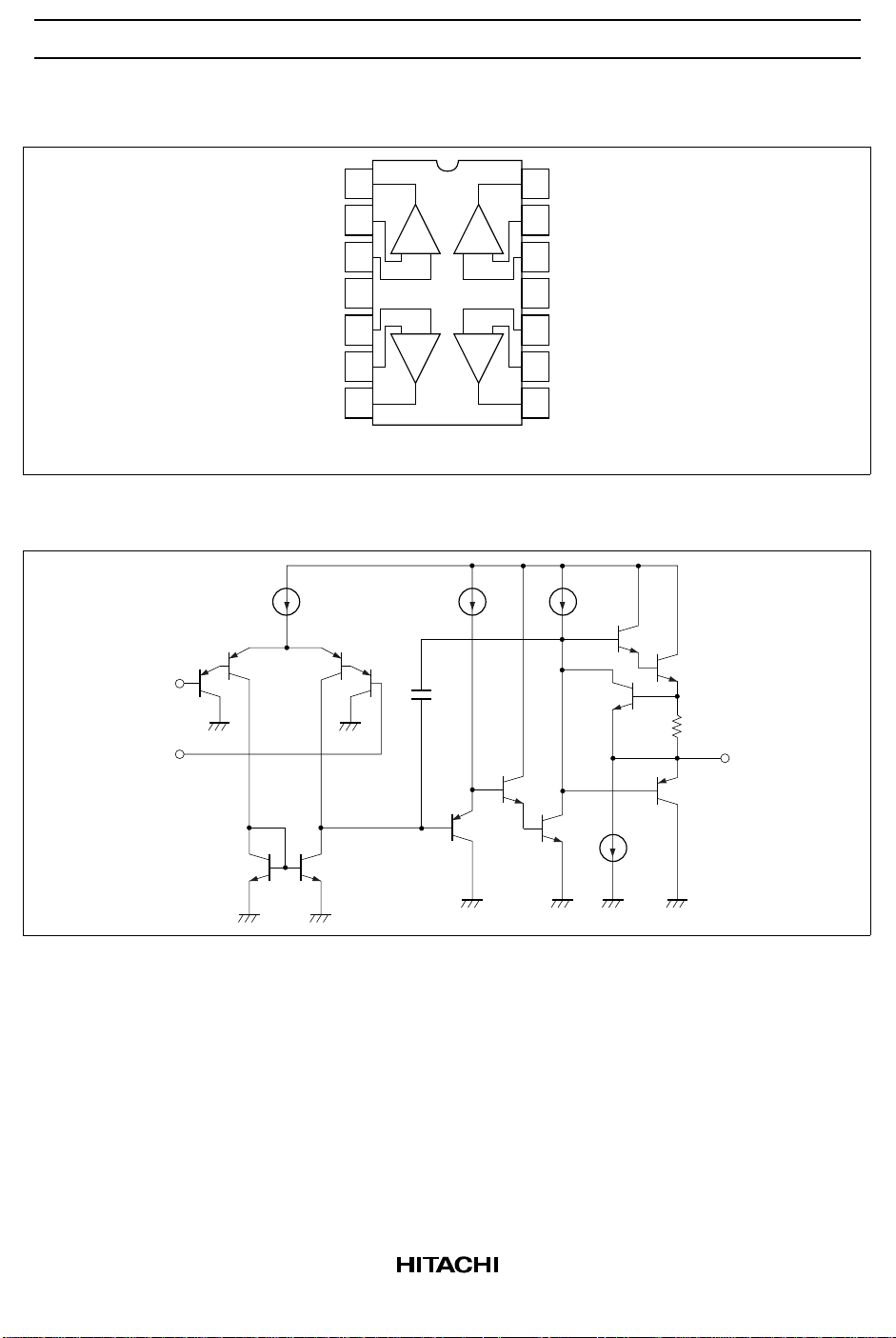
Pin Arrangement
Circuit Structure (1/4)
Q
Vin(–)
Vin(+)
Q
1
2
Vout1
Vin(–)1
Vin(+)1
V
CC
Vin(+)2
Vin(–)2
Vout2
Q
1
2
–+ +–
3
4
5
–+ +–
23
6
7
14
Vout4
13
12
11
10
9
8
Vin(–)4
Vin(+)4
GND
Vin(+)3
Vin(–)3
Vout3
41
(Top view)
Q
5
3
Q
4
C
Q
Q
6
7
R
1
Vout
Q
11
Q
10
Q
12
Q
13
Q
8
Q
9
2
Page 3
Absolute Maximum Ratings (Ta = 25°C)
HA17902 Series
Item Symbol HA17902/PHA17902PJHA17902FPHA17902
FPJ
Power supply
V
CC
28 28 28 28 28 V
HA17902
FPK
Unit
voltage
Sink current Io sink 50 50 50 50 25 mA
Allowable power
P
T
625*
1
625*
1
625*
2
625*
2
625*
2
mW
dissipation
Common-mode
input voltage
Differential-mode
V
CM
–0.3 to
V
Vin(diff) ±V
–0.3 to
CC
CC
V
±V
CC
CC
–0.3 to
V
CC
±V
CC
–0.3 to
V
CC
±V
CC
–0.3 to
V
CC
±V
CC
V
V
input voltage
Operating
temperature
Storage
temperature
Topr –20 to +75 –40 to +85 –20 to +75 –40 to +85 –40 to
+125
Tstg –55 to
+125
–55 to
+125
–55 to
+125
–55 to
+125
–55 to
+150
°C
°C
Notes: 1. These are the allowable values up to Ta = 50°C. Derate by 8.3mW/°C above that temperature.
2. See notes on SOP Package Usage in Reliability section.
3
Page 4
HA17902 Series
Electrical Characteristics 1 (VCC = + 15V, Ta = 25°C)
Item Symbol Min Typ Max Unit Test Conditions
Input offset voltage V
Input offset current I
Input bias current I
Power-supply
IO
IO
IB
PSRR — 93 — dB f = 100Hz, RS = 1kΩ, Rf = 100kΩ
—38mVV
— 5 50 nA IIO = | I
— 30 500 nA VCM = 7.5V
rejection ratio
Voltage gain A
Common-mode
VD
CMR — 80 — dB RS = 50Ω, Rf = 5kΩ
75 90 — dB RS = 1kΩ, Rf = 100kΩ, RL = ∞
rejection ratio
Common-mode input
V
CM
–0.3 — 13.5 V RS = 1kΩ, Rf = 100kΩ, f = 100Hz
voltage range
Maximum output
V
OP-P
— 13.6 — V f = 100Hz, RS = 1kΩ, Rf = 100kΩ,
voltage amplitude
Output voltage V
OH1
V
OH2
V
OL1
V
OL2
13.2 13.6 — V IOH = –1mA
12 13.3 — V IOH = –10mA
— 0.8 1 V IOL = 1mA
— 1.1 1.8 V IOL = 10mA
Output source current Io source 15 — — mA VOH = 10V
Output sink current Io sink 3 9 — mA VOL = 1V
Supply current I
CC
— 0.8 2 mA Vin = GND, RL = ∞
Slew rate SR — 0.19 — V/µs f = 1.5kHz, VCM = 7.5V, RL = ∞
Channel separation CS — 120 — dB f = 1kHz
= 7.5V, RS = 50Ω, Rf = 5kΩ
CM
–
+
– I
|, VCM = 7.5V
I
I
R
= 20kΩ
L
Electrical Characteristics 2 (VCC = + 15V, Ta = – 40 to 125°C)
Item Symbol Min Typ Max Unit Test Conditions
Input offset voltage V
Input offset current I
Input bias current I
Common-mode input
voltage range
Output voltage V
Supply current I
4
IO
IO
IB
V
CM
OH
V
OL
CC
——8 mVV
— — 200 nA VCM = 7.5V , IIO = | I
— — 500 nA VCM = 7.5V
0 — 13.0 V RS = 1kΩ, Rf = 100kΩ, f = 100Hz
13.0 ——VIOH = –1mA
——1.3VI
— — 4 mA Vin = GND, RL = ∞
= 7.5V, RS = 50Ω, Rf = 5kΩ
CM
= 1mA
OL
I
–
– I
+
|
I
Page 5
HA17902 Series
Test Circuits
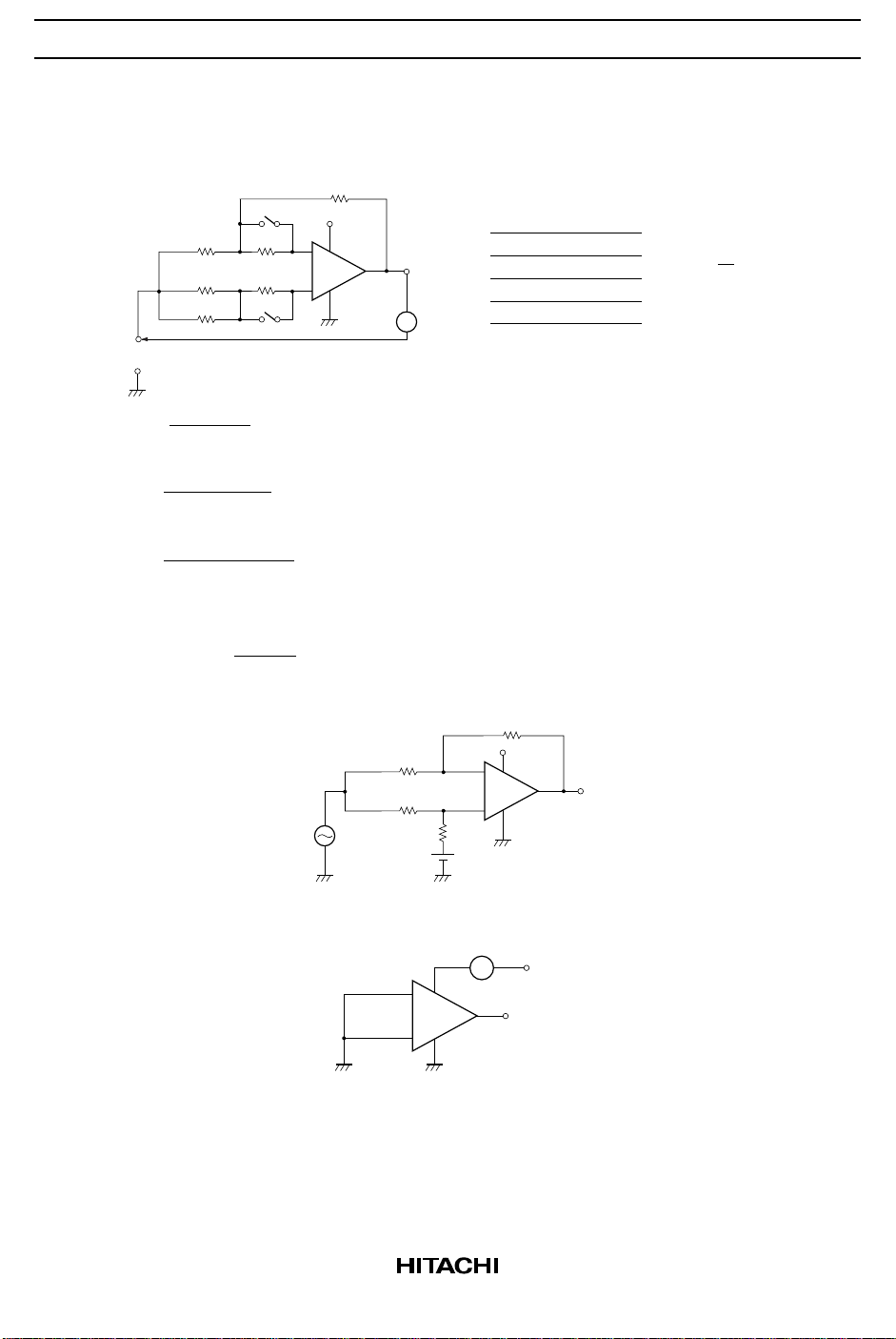
1. Input offset voltage (VIO), input offset current (IIO), and Input bias current (IIB) test circuit
Rf 5k
V
CM
VIO =
1 + Rf / R
V
IIO =
R(1 + Rf / RS)
IIB =
2 · R(1 + Rf / R
R
S
R
S
Rf 5k
V
O2
| V
O4
50
50
O1
– V
– VO3 |
R 10k
R 10k
SW2
S
O1
SW1
)
S
V
–
+
(mV)
(nA)
(nA)
CC
V
Vout
SW1
On
Off
On
Off
SW2
On
Off
Off
On
V
O
V
O1
V
O2
V
O3
V
O4
VCM =
1
2
V
CC
2. Common-mode rejection ratio (CMR) test circuit
V
· Rf
CMR = 20 log
IN
V
· R
O
S
Vin
(dB)
R
50
S
50
R
S
3. Supply current (ICC) test circuit
–
+
Rf
5.0k
Rf 5.0k
–
+
A
V
CC
Vout
Vout
V
CC
5
Page 6

HA17902 Series
4. Voltage gain (AVD), slew rate (SR), common-mode input voltage range (VCM), and maximum output
voltage amplitude (V
) test circuit.
OP-P
Vin
Vin
40dB
47µ
–
Rf
100k
R
51k
+
R
R
S
S
1k
1k
V
2
+
–
–
D.U.T
+
Rf
100k
V
1
V
CC
Vout
SW1
+
–
Rf
20k
47µ47µ
(1) A
(2) SR: f = 1.5kHz, RL = ∞, V1 = V2 = 1/2 V
: RS = 1kΩ, Rf = 100kΩ, RL = ∞, V1 = V2 = 1/2 V
VD
V
AVD = 20 log + 40
O
V
IN
(dB)
CC
V
CC
SR =
V
T
T
(3) VCM:RS = 1kΩ, Rf = 100kΩ, f = 100Hz, V1 = 1/2 VCC, RL = ∞,
and the value of V2 just slightly prior to the point where the output waveform changes.
(4) V
= 1kΩ, Rf = 100kΩ, RL: 20kΩ, f = 100Hz, V
OP-P:RS
= VOH ↔ VOL [V
OP-P
5. Output source current (Iosource) test circuit
Io source: VOH = 10V
V
10k
+
–
CC
V
OH
A
[V/µs]
P-P
]
6. Output sink current (Iosink) test circuit
Io sink: VOL = 1V
6
10k
V
CC
–
V
OH
+
A
Page 7

Characteristics Curve
HA17902 Series
Input Bias Current vs.
Power-Supply
100
(nA)
IB
75
50
25
Voltage Characteristics
Ta = 25°C
Vin = 7.5 V
Input Bias Current I
0
10 20 30
Power-Supply Voltage VCC (V)
Output Sink Current vs.
Ambient Temperature Characteristics
90
80
70
(mA)
60
o sink
50
40
30
20
Output Sink Current I
10
0
–55 –15 85 125
–35 5 25 45 65 105 –55 –15 85 125
VCC = 15 V
V
OH
Ambient Temperature Ta (°C)
= 1 V
Input Bias Current vs.
Ambient
90
80
70
(nA)
IB
60
50
40
30
20
Input Bias Current I
10
Temperature Characteristics
0
–55 –35 125
–15 5 25 45 65 85 105
Ambient Temperature Ta (°C)
Output Source Current vs.
Ambient Temperature Characteristics
90
80
(mA)
70
60
o source
50
40
30
20
Output Sink Current I
10
0
–35 5 25 45 65 105
VCC = 15 V
V
OH
Ambient Temperature Ta (°C)
= 10 V
7
Page 8

HA17902 Series
Voltage Gain vs.
160
140
120
(dB)
100
VD
80
60
40
Voltage Gain A
20
0
Frequency Characteristics
VCC = 15 V
Ta = 25°C
110 1 M
100 1 k 10 k 100 k 30
Frequency f (Hz)
Maximum Output Voltage Amplitude vs.
Frequency Characteristics
20
15
)
P-P
(V
10
OP-P
V
5
Power-Supply Voltage Characteristics
160
140
120
(dB)
100
VD
80
60
40
Voltage Gain A
20
0
10 20
Power-Supply Voltage VCC (V)
Supply Current vs.
Power-Supply Voltage Characteristics
4
3
(mA)
CC
2
1
Supply Current I
Voltage Gain vs.
Ta = 25°C
Ta = 25°C
Vin = GND
Maximum Output Voltage Amplitude
0
1 k
10 k 100 k
Frequency f (Hz)
8
1 M
0
10 20
Power-Supply Voltage VCC (V)
30
Page 9

HA17902 Series
Power-Supply Voltage Characteristics
Slew Rate vs.
0.8
0.6
0.4
Slew Rate SR (V/µs)
0.2
0
10 20
Power-Supply Voltage VCC (V)
V1 = V2 = 1/2 V
f = 1.5 kHz
Common-Mode Rejection Ratio vs.
Frequency Characteristics
120
CC
100
80
60
VCC = 15 V
Ta = 25°C
R
= 50 Ω
S
CMR (dB)
40
20
Common-Mode Rejection Ratio
30
0
100 100 k
1 k 10 k
1 M
Frequency f (Hz)
9
Page 10

HA17902 Series
Power-Supply Voltage Characteristics
Slew Rate vs.
0.8
0.6
0.4
Slew Rate SR (V/ s)
0.2
0
10 20
Power-Supply Voltage VCC (V)
V1 = V2 = 1/2 V
f = 1.5 kHz
Common-Mode Rejection Ratio vs.
Frequency Characteristics
120
CC
100
80
60
VCC = 15 V
Ta = 25¡C
= 50 Ω
R
S
CMR (dB)
40
20
Common-Mode Rejection Ratio
30
0
100 100 k
1 k 10 k
1 M
Frequency f (Hz)
10
Page 11

HA17902 Series
HA17902 Application Examples
The HA17902 is a quad operational amplifier, and consists of four operational amplifier circuits and one
bias current circuit. It features single-voltage power supply operation, internal phase compensation, a wide
zero-cross bandwidth, a low input bias current, and a high open-loop gain. Thus the HA17902 can be used
in a wide range of applications. This section describes several applications using the HA17902.
1. Noninverting Amplifier
Figure 1 shows the circuit diagram for a noninverting amplifier. The voltage gain of this amplifier is
given by the following formula.
= 1 +
R2
R1
Vout
Vin
+Vin
10k
10k
+
Vout
–
R
2
1M
R
1
Figure 1 Noninverting Amplifier
2. Summing Amplifier
Since the circuit shown in figure 2 applies +V1 and +V2 to the noninverting input and +V3 and +V4 to
the inverting input, the total output will be Vout = V1 + V2 – V3 – V4.
R
+V
+V
+V
+V
100k
1
R
100k
2
R
100k
3
R
100k
4
Vin(+)
100k
Vin(–)
+
HA17902
–
R
100 k
V
CC
Vout
Figure 2 Summing Amplifier
11
Page 12

HA17902 Series
3. High Input Impedance DC Differential Amplifier
The circuit shown in figure 3 is a high input impedance DC differential amplifier. This circuit’s
common-mode rejection ratio (CMR) depends on the matching between the R1/R2 and R4/R3 resistance
ratios. This amplifier’s output is given by the following formula.
R
Vout = 1 + (V2 – V1)
4
R
3
R
2
R
100kΩ 100kΩ
1
–
100kΩ
V
1
V
2
+
R
100kΩ
R
4
3
–
+
Vout
Figure 3 High Input Impedance DC Differential Amplifier
4. Voltage Controlled Oscillator
Figure 4 shows an oscillator circuit in which the amplifier A1 is an integrator, the amplifier A2 is a
comparator, and transistor Q1 operates as a switch that controls the oscillator frequency. If the output
Vout1 is at the low level, this will cut off transistor Q1 and cause the A1 inverting input to go to a higher
potential than the noninverting input. Therefore, A1 will integrate this negative input state and its output
level will decrease. When the A1 integrator output becomes lower than the A2 comparator noninverting
input level (VCC/2) the comparator output goes high. This turns on transistor Q1 causing the integrator to
integrate a positive input state and for its output to increase. This operation generates a square wave on
Vout1 and a triangular wave on Vout2.
+V
C 0.05µF
–
HA17902
+
V
CC
A
1
R
100k
C
51k
R/2
51k
50k
Q
1
10k
100k
V
CC
A
–
2
HA17902
/2
V
CC
+
Vout1
Vout2
12
Figure 4 Voltage Controlled Oscillator
Page 13

Package Dimensions
1
19.20
20.32 Max
1.30
HA17902 Series
Unit: mm
814
6.30
7.40 Max
7
2.54 ± 0.25
10.5 Max
14
1
1.27
2.39 Max
10.06
1.42 Max
0.48 ± 0.10
8
5.5
7
2.20 Max
2.54 Min 5.06 Max
0.51 Min
Hitachi Code
JEDEC
EIAJ
Mass
7.80
0.20 ± 0.04
*0.22 ± 0.05
0.70 ± 0.20
7.62
+ 0.10
0.25
– 0.05
0° – 15°
(reference value)
+ 0.20
– 0.30
1.15
0° – 8°
DP-14
Conforms
Conforms
0.97 g
Unit: mm
*0.42 ± 0.08
0.40 ± 0.06
*Dimension including the plating thickness
Base material dimension
0.12
0.10 ± 0.10
0.15
M
Hitachi Code
JEDEC
EIAJ
Mass
(reference value)
FP-14DA
—
Conforms
0.23 g
13
Page 14

HA17902 Series
Cautions
1. Hitachi neither warrants nor grants licenses of any rights of Hitachi’s or any third party’s patent,
copyright, trademark, or other intellectual property rights for information contained in this document.
Hitachi bears no responsibility for problems that may arise with third party’s rights, including
intellectual property rights, in connection with use of the information contained in this document.
2. Products and product specifications may be subject to change without notice. Confirm that you have
received the latest product standards or specifications before final design, purchase or use.
3. Hitachi makes every attempt to ensure that its products are of high quality and reliability. However,
contact Hitachi’s sales office before using the product in an application that demands especially high
quality and reliability or where its failure or malfunction may directly threaten human life or cause risk
of bodily injury, such as aerospace, aeronautics, nuclear power, combustion control, transportation,
traffic, safety equipment or medical equipment for life support.
4. Design your application so that the product is used within the ranges guaranteed by Hitachi particularly
for maximum rating, operating supply voltage range, heat radiation characteristics, installation
conditions and other characteristics. Hitachi bears no responsibility for failure or damage when used
beyond the guaranteed ranges. Even within the guaranteed ranges, consider normally foreseeable
failure rates or failure modes in semiconductor devices and employ systemic measures such as failsafes, so that the equipment incorporating Hitachi product does not cause bodily injury, fire or other
consequential damage due to operation of the Hitachi product.
5. This product is not designed to be radiation resistant.
6. No one is permitted to reproduce or duplicate, in any form, the whole or part of this document without
written approval from Hitachi.
7. Contact Hitachi’s sales office for any questions regarding this document or Hitachi semiconductor
products.
Hitachi, Ltd.
Semiconductor & Integrated Circuits.
Nippon Bldg., 2-6-2, Ohte-machi, Chiyoda-ku, Tokyo 100-0004, Japan
Tel: Tokyo (03) 3270-2111 Fax: (03) 3270-5109
URL NorthAmerica : http:semiconductor.hitachi.com/
For further information write to:
Hitachi Semiconductor
(America) Inc.
179 East Tasman Drive,
San Jose,CA 95134
Tel: <1> (408) 433-1990
Fax: <1>(408) 433-0223
Europe : http://www.hitachi-eu.com/hel/ecg
Asia (Singapore) : http://www.has.hitachi.com.sg/grp3/sicd/index.htm
Asia (Taiwan) : http://www.hitachi.com.tw/E/Product/SICD_Frame.htm
Asia (HongKong) : http://www.hitachi.com.hk/eng/bo/grp3/index.htm
Japan : http://www.hitachi.co.jp/Sicd/indx.htm
Hitachi Europe GmbH
Electronic components Group
Dornacher Straβe 3
D-85622 Feldkirchen, Munich
Germany
Tel: <49> (89) 9 9180-0
Fax: <49> (89) 9 29 30 00
Hitachi Europe Ltd.
Electronic Components Group.
Whitebrook Park
Lower Cookham Road
Maidenhead
Berkshire SL6 8YA, United Kingdom
Tel: <44> (1628) 585000
Fax: <44> (1628) 778322
Hitachi Asia Pte. Ltd.
16 Collyer Quay #20-00
Hitachi Tower
Singapore 049318
Tel: 535-2100
Fax: 535-1533
Hitachi Asia Ltd.
Taipei Branch Office
3F, Hung Kuo Building. No.167,
Tun-Hwa North Road, Taipei (105)
Tel: <886> (2) 2718-3666
Fax: <886> (2) 2718-8180
Copyright ' Hitachi, Ltd., 1998. All rights reserved. Printed in Japan.
14
Hitachi Asia (Hong Kong) Ltd.
Group III (Electronic Components)
7/F., North Tower, World Finance Centre,
Harbour City, Canton Road, Tsim Sha Tsui,
Kowloon, Hong Kong
Tel: <852> (2) 735 9218
Fax: <852> (2) 730 0281
Telex: 40815 HITEC HX
 Loading...