

Page 1

HA17901, HA17339 Series
Quadruple Comparators
Description
The HA17901 and HA17339 series products are comparators designed for use in power or control systems.
These IC operate from a single power-supply voltage over a wide range of voltages, and feature a reduced
power-supply current since the power-supply voltage is determined independently.
These comparators have the unique characteristic of ground being included in the common-mode input
voltage range, even when operating from a single-voltage power supply. These products have a wide range
of applications, including limit comparators, simple A/D converters, pulse/square-wave/time delay
generators, wide range VCO circuits, MOS clock timers, multivibrators, and high-voltage logic gates.
Features
• Wide power-supply voltage range: 2 to 36V
• Extremely low current drain: 0.8mA
• Low input bias current: 25nA
• Low input offset current: 5nA
• Low input offset voltage: 2mV
• The common-mode input voltage range includes ground.
• Low output saturation voltage: 1mV (5µA), 70mV (1mA)
• Output voltages compatible with CMOS logic systems
Page 2
HA17901, HA17339 Series
Ordering Information
Type No. Application Package
HA17901PJ Car use DP-14
HA17901FPJ FP-14DA
HA17901FPK FP-14DA
HA17901P Industrial use DP-14
HA17901FP FP-14DA
HA17339 Commercial use DP-14
HA17339F FP-14DA
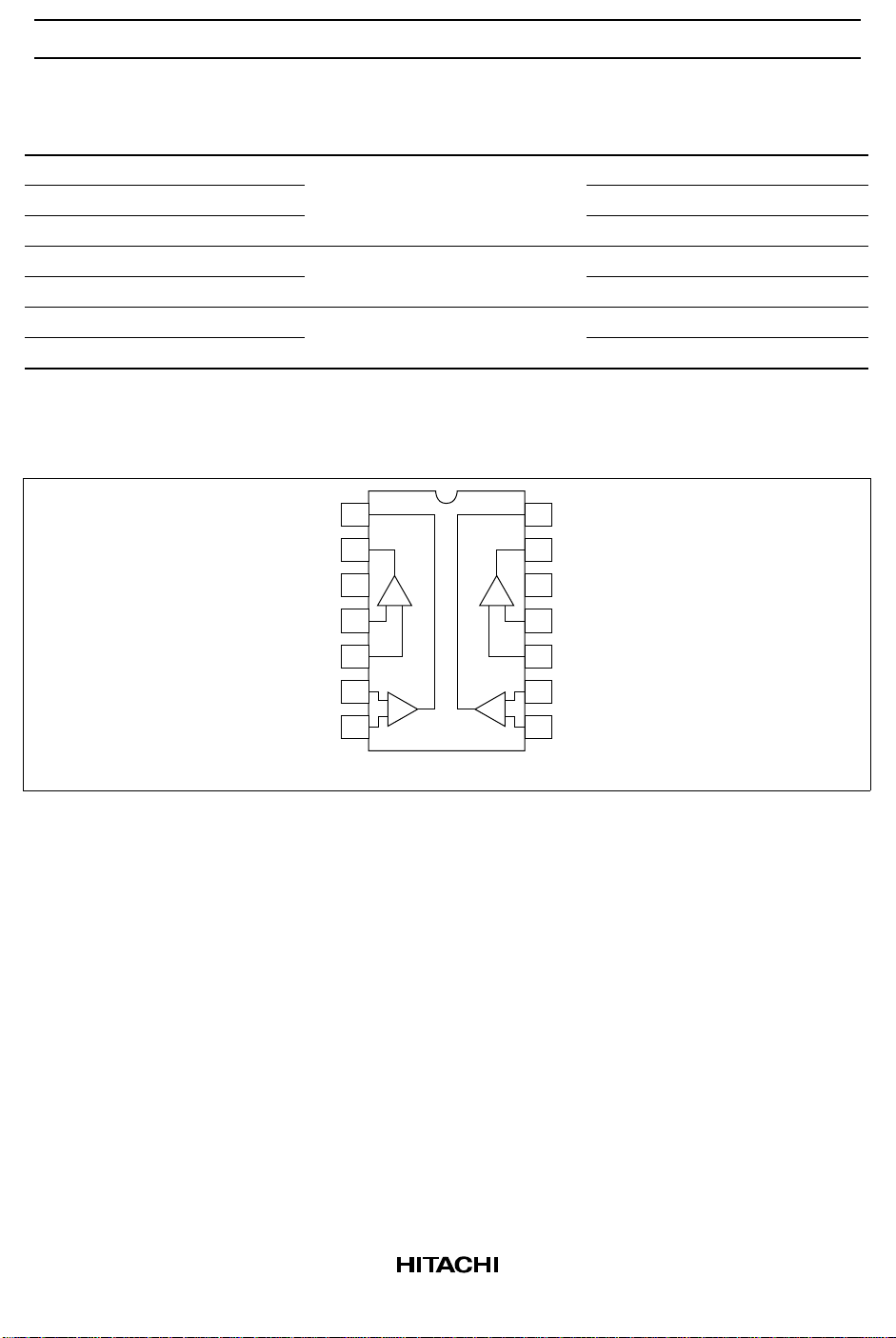
Pin Arrangement
Vout2
Vout1
V
CC
Vin(–)1
Vin(+)1
Vin(–)2
Vin(+)2
1
2
3
1
+
–
4
–
4
5
6
–
2
+
7
+
3
–
Vout3
14
Vout4
13
GND
12
+
Vin(+)4
11
Vin(–)4
10
Vin(+)3
9
Vin(–)3
8
(Top view)
2
Page 3
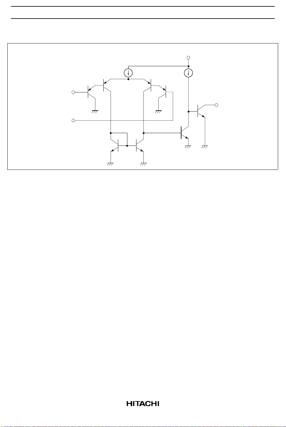
Circuit Structure (1/4)
HA17901, HA17339 Series
V
CC
Vin(–)
Q
2
Q
1
Q
3
Q
4Vin(+)
Vout
Q
8
Q
7
Q
5
Q
6
3
Page 4
HA17901, HA17339 Series
Absolute Maximum Ratings (Ta = 25°C)
Item Symbol
Power-
V
CC
17901
P
36 36 36 36 36 36 36 V
17901
PJ
17901FP17901
FPJ
17901
FPK
17339 17339
F Unit
supply
voltage
Differential
Vin(diff) ±V
CC
±V
CC
±V
CC
±V
CC
±V
CC
±V
CC
±V
CC
V
input
voltage
Input
voltage
Output
Vin –0.3 to
+V
CC
2
Iout*
20 20 20 20 20 20 20 mA
–0.3 to
+V
CC
–0.3 to
+V
CC
–0.3 to
+V
CC
–0.3 to
+V
CC
–0.3 to
+V
CC
–0.3 to
+V
CC
V
current
Allowable
P
T
625*
1
625*
1
625*
3
625*
3
625*
3
625*
1
625*
3
mW
power
dissipation
Operating
temperature
Storage
temperature
Output pin
Topr –20 to
+75
Tstg –55 to
+125
–40 to
+85
–55 to
+125
–20 to
+75
–55 to
+125
–40 to
+85
–55 to
+125
–40 to
+125
–55 to
+150
–20 to
+75
–55 to
+125
–20 to
+75
–55 to
+125
Vout 36 36 36 36 36 36 36 V
°C
°C
voltage
Notes: 1. These are the allowable values up to Ta = 50°C. Derate by 8.3mW/°C above that temperature.
2. These products can be destroyed if the output and V
are shorted together. The maximum
CC
output current is the allowable value for continuous operation.
3. See notes of SOP Package Usage in Reliability section.
4
Page 5
HA17901, HA17339 Series
Electrical Characteristics 1 (VCC = 5V, Ta = 25°C)
Item Symbol Min Typ Max Unit Test Condition
Input offset
V
IO
voltage
Input bias current I
Input offset
IB
I
IO
current
Common-mode
input voltage*
Supply current I
Voltage Gain A
Response time*2t
Output sink
V
1
CM
CC
VD
R
Iosink 6 16 — mA V
current
Output saturation
VO sat — 200 400 mV V
voltage
Output leakage
I
LO
current
Notes: 1. Voltages more negative than –0.3V are not allowed for the common-mode input voltage or for
either one of the input signal voltages.
2. The stipulated response time is the value for a 100 mV input step voltage that has a 5mV
overdrive.
— 2 7 mV Output switching point: when
V
= 1.4V, RS = 0Ω
O
— 25 250 nA I
— 5 50 nA I
0—V
– 1.5 V
CC
IN(+)
IN(+)
or I
– I
IN(–)
IN(–)
— 0.8 2 mA RL = ∞
— 200 — V/mV RL = 15kΩ
— 1.3 — µsVRL = 5V, RL = 5.1kΩ
= 1V, V
IN(–)
= 1V, V
IN(–)
= 0, VO ≤ 1.5V
IN(+)
= 0, Iosink =
IN(+)
3mA
— 0.1 — nA V
= 1V, V
IN(+)
= 0, VO = 5V
IN(–)
Electrical Characteristics 2 (VCC = 5V, Ta = – 41 to + 125°C)
Item Symbol Min Typ Max Unit Test Condition
Input offset
V
IO
voltage
Input offset
I
IO
current
Input bias current I
Common-mode
input voltage*
1
Output saturation
IB
V
VO
CM
sat
voltage
Output leakage
I
LO
current
Supply current I
CC
Note: 1. Voltages more negative than –0.3V are not allowed for the common-mode input voltage or for
either one of the input signal voltages.
— — 7 mV Output switching point: when
V
= 1.4V, RS = 0Ω
O
— — 200 nA I
IN(-)
– I
IN(+)
— — 500 nA
0—V
— — 440 mV V
– 2.0 V
CC
≥ 1V, V
IN(–)
= 0, Iosink ≤
IN(+)
4mA
— 1.0 — µAV
= 0V, V
IN(–)
≥ 1V, VO = 30V
IN(+)
— — 4.0 mA All comparators: RL = ∞,
All channels ON
5
Page 6

HA17901, HA17339 Series
Test Circuits
1. Input offset voltage (VIO), input offset current (IIO), and Input bias current (IIB) test circuit
Rf 5k
V
(mV)
(nA)
(nA)
CC
RL 51k
–
470µ
+
–
V
+
SW1
On
Off
V
O
On
Off
SW2
On
Off
Off
On
Vout
V
O1
V
O2
V
O3
V
O4
VC1 =
VC2 = 1.4V
R
R
V
C1
VIO =
1 + Rf / R
| V
IIO =
R(1 + Rf / R
IIB =
2 · R(1 + Rf / R
S
S
| V
50
50
| V
O2
|
O1
– VO1 |
– VO3 |
O4
SW1
R 20 k
R 20 k
Rf 5 k
V
C2
S
S
SW2
)
)
S
1
V
CC
2
2. Output saturation voltage (VO sat) output sink current (Iosink), and common-mode input voltage (VCM)
test circuit
V
SW1
V
V
CC
50
SW2
1
1
2
2
C1
5k
50 50
C2
1.6k
−
+
4.87k
SW3
Item
V
V
V
C3
C1
sat
2V
O
V
0V
C2
V
SW11SW21SW3
C3
—
1 at
V
3 at
V
CC
CC
Iosink 2V 0V 1.5V 1 1 2 mA
V
CM
2V –1 to
V
CC
—2
Switched
between
1 and 2
3V
= 5V
= 15V
Unit
V
3. Supply current (ICC) test circuit
1V
A
+
–
V
CC
ICC: RL = ∞
6
Page 7

4. Voltage gain (AVD) test circuit (RL = 15kΩ)
AVD = 20 log
+V
20k
10k
20k
–V
V
— V
O1
O2
V
— V
IN1
(dB)
IN2
30k
Vin
10µ
+
–
V
CC
RL 15k
+
–
5050
5. Response time (tR) test circuit
V
CC
RL 5.1k
50
–
+
SW120k
24k
VR
5 k
+V
–V
Vin
50
P.G
30k
tR: RL = 5.1kΩ, a 100mV input step voltage that has a 5mV overdrive
HA17901, HA17339 Series
V
O
V
O
12V
• With VIN not applied, set the switch SW to the off position and adjust VR so that VO is in the vicinity of
1.4V.
• Apply VIN and turn the switch SW on.
90%
10%
t
R
7
Page 8

HA17901, HA17339 Series
Characteristics Curve
Input Bias Current vs.
Ambient Temperature Characteristics
90
80
70
(nA)
IB
60
50
40
30
20
Input Bias Current I
10
0
–55 –15 45 85 125
–35 5 25 65 105
VCC = 5 V
Ambient Temperature Ta (°C)
Supply Current vs.
Ambient Temperature Characteristics
1.8
1.6
1.4
(mA)
1.2
CC
1.0
0.8
0.6
0.4
Supply Current I
0.2
0
–55 –15 45 85 125
–35 5 25 65 105
VCC = 5 V
R
Ambient Temperature Ta (°C)
= ∞
L
Input Bias Current vs.
Power-Supply Voltage Characteristics
60
50
(nA)
IB
40
30
20
10
Input Bias Current I
010203040
Ta = 25°C
Power-Supply Voltage VCC (V)
Supply Current vs.
Power-Supply Voltage Characteristics
1.6
1.4
(mA)
1.2
CC
1.0
0.8
Supply Current I
0.6
010203040
Ta = 25°C
R
= ∞
L
Power-Supply Voltage VCC (V)
8
Page 9

HA17901, HA17339 Series
Output Sink Current vs.
Ambient Temperature Characteristics
45
40
35
30
25
20
15
10
5
Output Sink Current Iosink (mA)
0
–55 –15 45 85 125
–35 5 25 65 105
VCC = 5 V
Vin(–) = 1 V
Vin(+) = 0
Vout = 1.5 V
Ambient Temperature Ta (°C)
Voltage Gain vs.
Ambient Temperature Characteristics
130
125
120
(dB)
115
VD
110
105
100
Voltage Gain A
95
90
85
–55 –15 45 85 125
–35 5 25 65 105
VCC = 5 V
= 15 kΩ
R
L
Ambient Temperature Ta (°C)
Output Sink Current vs.
Power-Supply Voltage Characteristics
30
25
20
15
10
5
Output Sink Current Iosink (mA)
0
010203040
Power-Supply Voltage VCC (V)
Voltage Gain vs.
Power-Supply Voltage Characteristics
130
120
(dB)
110
VD
100
90
Voltage Gain A
80
70
010203040
Ta = 25°C
= 15 kΩ
R
L
Power-Supply Voltage VCC (V)
9
Page 10

HA17901, HA17339 Series
HA17901 Application Examples
The HA17901 houses four independent comparators in a single package, and operates over a wide voltage
range at low power from a single-voltage power supply. Since the common-mode input voltage range starts
at the ground potential, the HA17901 is particularly suited for single-voltage power supply applications.
This section presents several sample HA17901 applications.
HA17901 Application Notes
1. Square-Wave Oscillator
The circuit shown in figure one has the same structure as a single-voltage power supply astable
multivibrator. Figure 2 shows the waveforms generated by this circuit.
V
CC
100k
R
V
75pF
C
V
CC
100k
CC
–
HA17901
+
4.3k
Vout
100k
Figure 1 Square-Wave Oscillator
(1)
Horizontal: 2 V/div, Vertical: 5 µs/div, VCC = 5 V
Figure 2 Operating Waveforms
100k
(2)
Horizontal: 5 V/div, Vertical: 5 µs/div, VCC = 15 V
10
Page 11

HA17901, HA17339 Series
2. Pulse Generator
The charge and discharge circuits in the circuit from figure 1 are separated by diodes in this circuit. (See
figure 3.) This allows the pulse width and the duty cycle to be set independently. Figure 4 shows the
waveforms generated by this circuit.
V
CC
R1 1M D1 IS2076
80pF
V
CC
Figure 3 Pulse Generator
Horizontal: 2 V/div, Vertical: 20 µs/div, V
Figure 4 Operating Waveforms
R2 100k
C
1M
= 5 V
CC
D2 IS2076
V
CC
–
HA17901
+
1M
1M
Horizontal: 5 V/div, Vertical: 20 µs/div, VCC = 15 V
Vout
3. Voltage Controlled Oscillator
In the circuit in figure 5, comparator A1 operates as an integrator, A2 operates as a comparator with
hysteresis, and A3 operates as the switch that controls the oscillator frequency. If the output Vout1 is at
the low level, the A3 output will go to the low level and the A1 inverting input will become a lower
level than the A1 noninverting input. The A1 output will integrate this state and its output will increase
towards the high level. When the output of the integrator A1 exceeds the level on the comparator A
inverting input, A2 inverts to the high level and both the output Vout1 and the A3 output go to the high
level. This causes the integrator to integrate a negative state, resulting in its output decreasing towards
the low level. Then, when the A1 output level becomes lower than the level on the A2 noninverting
input, the output Vout1 is once again inverted to the low level. This operation generates a square wave
on Vout1 and a triangular wave on Vout2.
2
11
Page 12

HA17901, HA17339 Series
100k
V
CC
A
+
HA17901
–
V
CC
3k
2
Output 1
Output 2
100k
+V
C
Frequency
control
voltage
input
V
= 30V
CC
+250mV < +VC < +50V
700Hz < / < 100kHz
50k
20k
0.1µ
10
20k
V
CC
A
–
HA17901
+
V
A
3
HA17901
1
CC
500p
–
+
0.01µ
VCC/2
3k
V
CC
5.1k
VCC/2
Figure 5 Voltage Controlled Oscillator
4. Basic Comparator
The circuit shown in figure 6 is a basic comparator. When the input voltage VIN exceeds the reference
voltage V
, the output goes to the high level.
REF
Vin
V
CC
+
3kΩ
V
REF
–
Figure 6 Basic Comparator
5. Noninverting Comparator (with Hysteresis)
Assuming +VIN is 0V, when V
is applied to the inverting input, the output will go to the low level
REF
(approximately 0V). If the voltage applied to +VIN is gradually increased, the output will go high when
the value of the noninverting input, +VIN × R2/(R1 + R2), exceeds +V
. Next, if +VIN is gradually
REF
lowered, Vout will be inverted to the low level once again when the value of the noninverting input,
(Vout – VIN) × R1/(R1 + R2), becomes lower than V
assuming VCC = 15V and +V
= 6V, the following formula can be derived, i.e. +VIN × 10M/(5.1M +
REF
. With the circuit constants shown in figure 7,
REF
10M) > 6V, and Vout will invert from low to high when +VIN is > 9.06V.
R
(Vout – VIN) ×
1
R1 + R
+ VIN < 6V
2
(Assuming Vout = 15V)
When +VIN is lowered, the output will invert from high to low when +VIN < 1.41V. Therefore this
circuit has a hysteresis of 7.65V. Figure 8 shows the input characteristics.
12
Page 13

HA17901, HA17339 Series
+V
REF
+Vin
V
–
R
HA17901
1
+
CC
V
CC
5.1M
10M
R
2
Figure 7 Noninverting Comparator
20
16
12
8
4
Output Voltage Vout (V)
0
0 5 10 15
VCC = 15 V, +V
+Vin = 0 to 10 V
REF
Input Voltage VIN (V)
= 6 V
3k
Vout
Figure 8 Noninverting Comparator I/O Transfer Characteristics
6. Inverting Comparator (with Hysteresis)
In this circuit, the output Vout inverts from high to low when +VIN > (VCC + Vout)/3. Similarly, the
output Vout inverts from low to high when +VIN < VCC/3. With the circuit constants shown in figure 9,
assuming VCC = 15V and Vout = 15V, this circuit will have a 5V hysteresis. Figure 10 shows the I/O
characteristics for the circuit in figure 9.
+Vin
V
CC
1M
HA17901
1M
V
CC
–
+
1M
V
CC
3k
Vout
Figure 9 Inverting Comparator
13
Page 14
HA17901, HA17339 Series
20
16
12
8
4
Output Voltage Vout (V)
0
0 5 10 15
Input Voltage VIN (V)
Figure 10 Inverting Comparator I/O Transfer Characteristics
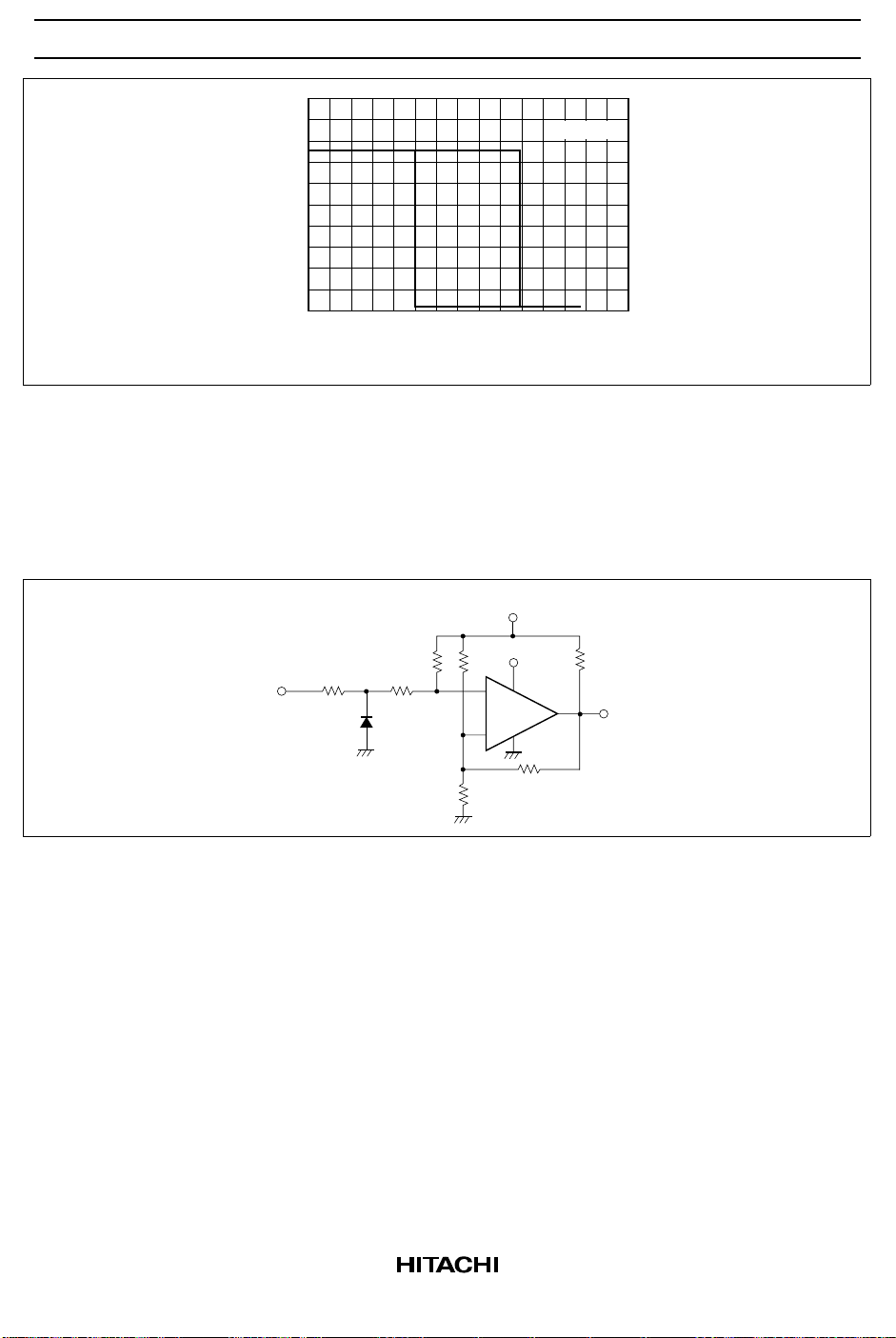
7. Zero-Cross Detector (Single-Voltage Power Supply)
In this circuit, the noninverting input will essentially beheld at the potential determined by dividing V
with 100kΩ and 10k Ω resistors. When VIN is 0V or higher, the output will be low, and when VIN is
negative, Vout will invert to the high level. (See figure 11.)
VCC = 15 V
CC
Vin
V
CC
V
–
HA17901
+
10k
CC
20M
5.1k5.1k
100k100k
1S2076
Figure 11 Zero-Cross Detector
5.1k
Vout
14
Page 15

Package Dimensions
1
19.20
20.32 Max
1.30
HA17901, HA17339 Series
Unit: mm
814
6.30
7.40 Max
7
2.54 ± 0.25
10.5 Max
14
1
1.27
2.39 Max
10.06
1.42 Max
0.48 ± 0.10
8
5.5
7
2.20 Max
2.54 Min 5.06 Max
0.51 Min
Hitachi Code
JEDEC
EIAJ
Mass
7.80
0.20 ± 0.04
*0.22 ± 0.05
0.70 ± 0.20
7.62
+ 0.10
0.25
– 0.05
0° – 15°
(reference value)
+ 0.20
– 0.30
1.15
0° – 8°
DP-14
Conforms
Conforms
0.97 g
Unit: mm
*0.42 ± 0.08
0.40 ± 0.06
*Dimension including the plating thickness
Base material dimension
0.12
0.10 ± 0.10
0.15
M
Hitachi Code
JEDEC
EIAJ
Mass
(reference value)
FP-14DA
—
Conforms
0.23 g
15
Page 16

HA17901, HA17339 Series
Cautions
1. Hitachi neither warrants nor grants licenses of any rights of Hitachi’s or any third party’s patent,
copyright, trademark, or other intellectual property rights for information contained in this document.
Hitachi bears no responsibility for problems that may arise with third party’s rights, including
intellectual property rights, in connection with use of the information contained in this document.
2. Products and product specifications may be subject to change without notice. Confirm that you have
received the latest product standards or specifications before final design, purchase or use.
3. Hitachi makes every attempt to ensure that its products are of high quality and reliability. However,
contact Hitachi’s sales office before using the product in an application that demands especially high
quality and reliability or where its failure or malfunction may directly threaten human life or cause risk
of bodily injury, such as aerospace, aeronautics, nuclear power, combustion control, transportation,
traffic, safety equipment or medical equipment for life support.
4. Design your application so that the product is used within the ranges guaranteed by Hitachi particularly
for maximum rating, operating supply voltage range, heat radiation characteristics, installation
conditions and other characteristics. Hitachi bears no responsibility for failure or damage when used
beyond the guaranteed ranges. Even within the guaranteed ranges, consider normally foreseeable
failure rates or failure modes in semiconductor devices and employ systemic measures such as failsafes, so that the equipment incorporating Hitachi product does not cause bodily injury, fire or other
consequential damage due to operation of the Hitachi product.
5. This product is not designed to be radiation resistant.
6. No one is permitted to reproduce or duplicate, in any form, the whole or part of this document without
written approval from Hitachi.
7. Contact Hitachi’s sales office for any questions regarding this document or Hitachi semiconductor
products.
Hitachi, Ltd.
Semiconductor & Integrated Circuits.
Nippon Bldg., 2-6-2, Ohte-machi, Chiyoda-ku, Tokyo 100-0004, Japan
Tel: Tokyo (03) 3270-2111 Fax: (03) 3270-5109
URL NorthAmerica : http:semiconductor.hitachi.com/
For further information write to:
Hitachi Semiconductor
(America) Inc.
179 East Tasman Drive,
San Jose,CA 95134
Tel: <1> (408) 433-1990
Fax: <1>(408) 433-0223
Europe : http://www.hitachi-eu.com/hel/ecg
Asia (Singapore) : http://www.has.hitachi.com.sg/grp3/sicd/index.htm
Asia (Taiwan) : http://www.hitachi.com.tw/E/Product/SICD_Frame.htm
Asia (HongKong) : http://www.hitachi.com.hk/eng/bo/grp3/index.htm
Japan : http://www.hitachi.co.jp/Sicd/indx.htm
Hitachi Europe GmbH
Electronic components Group
Dornacher Straβe 3
D-85622 Feldkirchen, Munich
Germany
Tel: <49> (89) 9 9180-0
Fax: <49> (89) 9 29 30 00
Hitachi Europe Ltd.
Electronic Components Group.
Whitebrook Park
Lower Cookham Road
Maidenhead
Berkshire SL6 8YA, United Kingdom
Tel: <44> (1628) 585000
Fax: <44> (1628) 778322
Hitachi Asia Pte. Ltd.
16 Collyer Quay #20-00
Hitachi Tower
Singapore 049318
Tel: 535-2100
Fax: 535-1533
Hitachi Asia Ltd.
Taipei Branch Office
3F, Hung Kuo Building. No.167,
Tun-Hwa North Road, Taipei (105)
Tel: <886> (2) 2718-3666
Fax: <886> (2) 2718-8180
Copyright ' Hitachi, Ltd., 1998. All rights reserved. Printed in Japan.
16
Hitachi Asia (Hong Kong) Ltd.
Group III (Electronic Components)
7/F., North Tower, World Finance Centre,
Harbour City, Canton Road, Tsim Sha Tsui,
Kowloon, Hong Kong
Tel: <852> (2) 735 9218
Fax: <852> (2) 730 0281
Telex: 40815 HITEC HX
 Loading...