

Page 1
HA17324 Series
Quad Operational Amplifier
Description
HA17324 is quad operational amplifier that provide high gain and internal phase compensation, with single
power supply. They can be widely used to control equipments.
Features
• Wide range of supply voltage, and single power supply used
• Internal phase compensation
• Wide range of common mode voltage, and possible to operate with an input about 0V
Ordering Information
Type No. Application Package
HA17324FP Industrial use FP-14DA
HA17324F Commercial use FP-14DA
HA17324 Commercial use DP-14
HA17324P Industrial use DP-14
Page 2
HA17324 Series
2
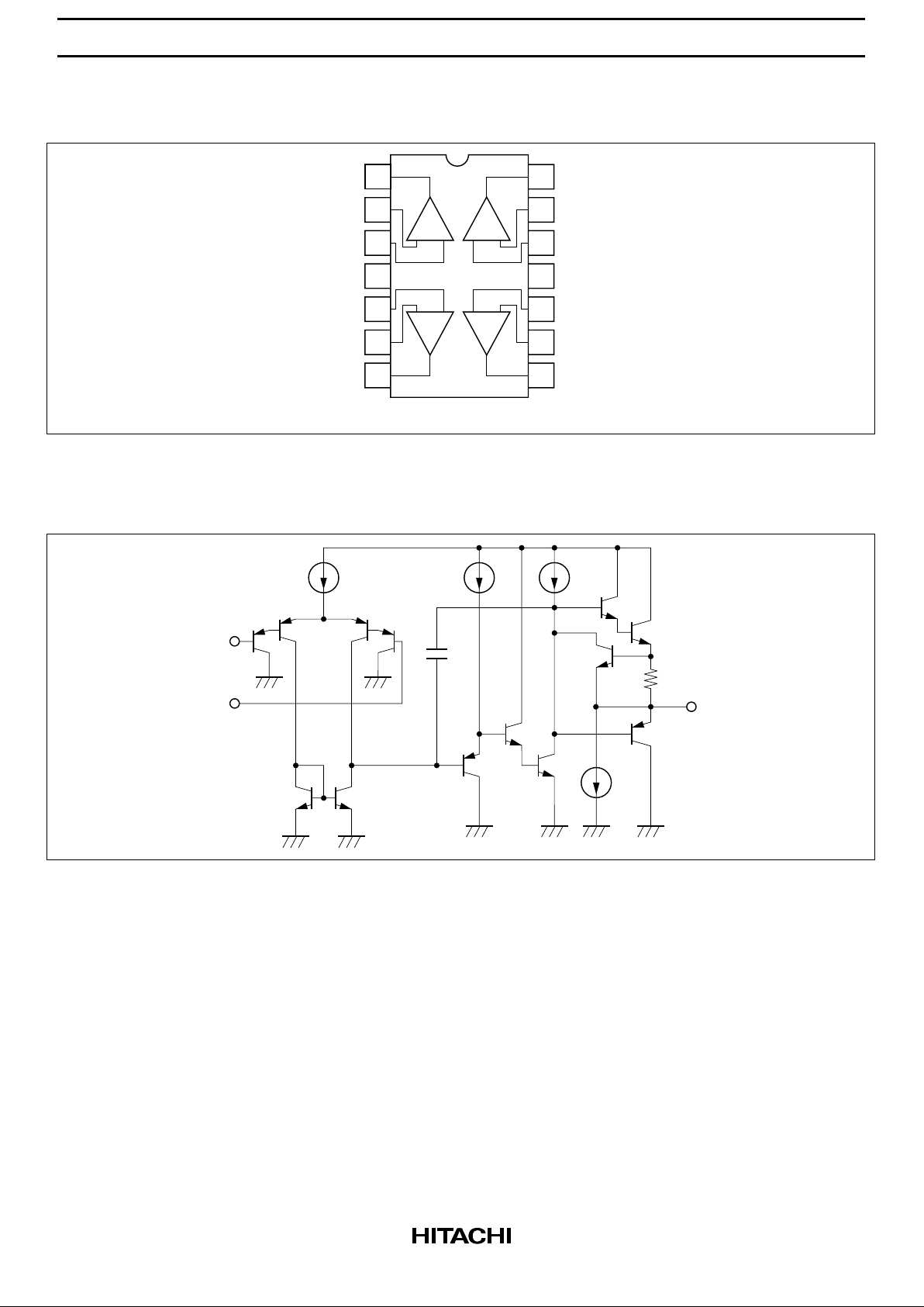
Pin Arrangement
Vout1
Vin(–)1
Vin(+)1
V
CC
Vin(+)2
Vin(–)2
Vout2
Vout4
Vin(–)4
Vin(+)4
V
EE
Vin(+)3
Vin(–)3
Vout3
–
1
+
2
(Top View)
1
3
2
3
4
5
6
7
14
13
12
11
10
9
8
+
4
–
–
+
+
–
Circuit Schematic (1/4)
Q1 Q4
Q2 Q3
Q5
Q6
Q7
Q13
Q12
Q11
Q10
Q8 Q9
Vout
R
1
Vin(+)
Vin(–)
C
Page 3
HA17324 Series
3
Absolute Maximum Ratings (Ta = 25°C)
Item Symbol Rating Unit
Supply voltage V
CC
32 V
Sink current Isink 50 mA
Power dissipation P
T
625* mW
Common mode input voltage V
CM
–0.3 to V
CC
V
Differential input voltage Vin (diff) ±V
CC
V
Operating temperature Topr –20 to +75 °C
Storage temperature Tstg –55 to +125 °C
Note: These are allowable values up to Ta=50°C.
Derate by 8.3mW/°C above that temperature.
In case of SOP, see notes on SOP Package Usage in Reliability section.
Page 4

HA17324 Series
4
Electrical Characteristics (VCC = +15V, Ta = 25°C)
Item Symbol Min Typ Max Unit Test Conditions
Input offset voltage V
IO
—2 7 mVV
CM
= 7.5V, RS = 50Ω, Rf = 50kΩ
Input offset current I
IO
— 5 50 nA VCM = 7.5V, IIO = | I
I (–)
– I
I (+)
|
Input bias current I
IB
— 30 500 nA VCM = 7.5V
Power source rejection
ratio
PSRR — 93 — dB f = 100Hz, RS = 1kΩ, Rj = 100kΩ
Voltage gain A
VD
75 90 — dB RS = 1 kΩ, Rf = 100kΩ, RL = ∞
Common mode rejection
ratio
CMR — 80 — dB RS = 50Ω, Rf = 5kΩ
Common mode input
voltage range
V
CM
–0.3 — 13.5 V RS = 1kΩ, Rf = 100kΩ, f = 100Hz
Maximum output voltage Vop-p — 13.6 — V f = 100Hz, RS = 1kΩ, Rf = 100kΩ,
R
L
= 20kΩ
Output source current Iosource 20 40 — mA V
IN
+
= 1V, V
IN
–
= 0V, VOH = 10V
Output sink current Iosink 10 20 — mA VIN = 0V, VIN = 1V, VOL = 2.5V
Supply current I
CC
— 0.8 2 mA VIN = GND, RL = ∞
Slew rate SR — 0.19 — V/µs f = 1.5kHz, VCM = 7.5V, RL = ∞
Channel separation CS — 120 — dB f = 1kHz
Output sink current Iosink 15 50 — µAV
IN
+
= 0V, V
IN
–
= 1V, VOL = 200mV
Iosink 3 9 — mA V
IN
+
= 0V, V
IN
–
= 1V, VOL = 1V
Output voltage V
OH
13.2 13.6 — V IOH = –1mA
V
OH
12.0 13.3 — V IOH = –10mA
Output voltage V
OL
— 0.8 1.0 V IOL = 1mA
V
OL
— 1.1 1.8 V IOL = 10mA
Page 5

HA17324 Series
5
Characteristic Curves
Output Source Current
vs. Ambient Temperature
80
Output Source Current Iosource (mA)
Ambeint Temperature Ta (°C)
70
60
50
40
30
20
10
0
–200 20406080
VCC = 15 V
V
OH
= 10 V
Input Bias Current
vs. Ambient Temperature
80
Input Bias Current I
IB
(nA)
Ambeint Temperature Ta (°C)
70
60
50
40
30
20
10
0
–200 20406080
VCC = 15 V
V
CM
= 7.5 V
Supply Current vs. Supply Voltage
4
Supply Current I
CC
(mA)
Supply Voltage VCC (V)
3
2
1
0
8 16243240
Ta = 25°C
Input Bias Current vs. Supply Voltage
80
Input Bias Current I
IB
(nA)
Supply Voltage VCC (V)
60
40
20
0
8 16243240
Ta = 25°C
Voltage Gain vs. Supply Voltage
160
Voltage Gain A
VD
(dB)
Supply Voltage VCC (V)
120
80
40
0
8 16243240
Ta = 25°C
R
L
= ∞
Maxlmum Output Voltage vs. Frequency
20
Maximum Output Voltage V
OP–P
(V)
Frequency f (Hz)
1 k 3 k 10 k 30 k 100 k 300 k
16
12
8
4
0
VCC = 15 V
Ta = 25°C
R
L
= 20 kΩ
1 M
Page 6

HA17324 Series
6
Voltage Gain vs. Frequency
V
CC
= 15V
Ta = 25°C
RL = ∞
Voltage Gain A
VD
(dB)
120
100
80
60
40
20
0
1 3 10 30 100 300 1 k 3 k 10 k 30 k 100 k 300 k 1 M
Frequency f (Hz)
V
CC
= 15V
Ta = 25°C
RS = 50 Ω
120
100
80
60
40
20
0
100 300 1 k 3 k 10 k 30 k 100 k 300 k 1M
Frequency f (Hz)
Common Mode Rejection Ratio vs. Frequency
Common Mode Rejection Ratio CMR (dB)
Page 7

HA17324 Series
7
Package Dimensions
Hitachi Code
JEDEC
EIAJ
Mass
(reference value)
DP-14
Conforms
Conforms
0.97 g
Unit: mm
7.62
0.25
0° – 15°
19.20
20.32 Max
1
814
7
1.30
2.54 ± 0.25
0.48 ± 0.10
6.30
7.40 Max
0.51 Min
2.54 Min 5.06 Max
+ 0.10
– 0.05
2.39 Max
Hitachi Code
JEDEC
EIAJ
Mass
(reference value)
FP-14DA
—
Conforms
0.23 g
Unit: mm
*Dimension including the plating thickness
Base material dimension
*0.22 ± 0.05
*0.42 ± 0.08
0.70 ± 0.20
0.12
0.15
0° – 8°
M
0.10 ± 0.10
2.20 Max
5.5
10.06
1.42 Max
14
8
1
7
10.5 Max
+ 0.20
– 0.30
7.80
1.15
1.27
0.40 ± 0.06
0.20 ± 0.04
Page 8

HA17324 Series
8
Cautions
1. Hitachi neither warrants nor grants licenses of any rights of Hitachi’s or any third party’s patent,
copyright, trademark, or other intellectual property rights for information contained in this document.
Hitachi bears no responsibility for problems that may arise with third party’s rights, including
intellectual property rights, in connection with use of the information contained in this document.
2. Products and product specifications may be subject to change without notice. Confirm that you have
received the latest product standards or specifications before final design, purchase or use.
3. Hitachi makes every attempt to ensure that its products are of high quality and reliability. However,
contact Hitachi’s sales office before using the product in an application that demands especially high
quality and reliability or where its failure or malfunction may directly threaten human life or cause risk
of bodily injury, such as aerospace, aeronautics, nuclear power, combustion control, transportation,
traffic, safety equipment or medical equipment for life support.
4. Design your application so that the product is used within the ranges guaranteed by Hitachi particularly
for maximum rating, operating supply voltage range, heat radiation characteristics, installation
conditions and other characteristics. Hitachi bears no responsibility for failure or damage when used
beyond the guaranteed ranges. Even within the guaranteed ranges, consider normally foreseeable
failure rates or failure modes in semiconductor devices and employ systemic measures such as failsafes, so that the equipment incorporating Hitachi product does not cause bodily injury, fire or other
consequential damage due to operation of the Hitachi product.
5. This product is not designed to be radiation resistant.
6. No one is permitted to reproduce or duplicate, in any form, the whole or part of this document without
written approval from Hitachi.
7. Contact Hitachi’s sales office for any questions regarding this document or Hitachi semiconductor
products.
Hitachi, Ltd.
Semiconductor & Integrated Circuits.
Nippon Bldg., 2-6-2, Ohte-machi, Chiyoda-ku, Tokyo 100-0004, Japan
Tel: Tokyo (03) 3270-2111 Fax: (03) 3270-5109
Copyright ' Hitachi, Ltd., 1998. All rights reserved. Printed in Japan.
Hitachi Asia Pte. Ltd.
16 Collyer Quay #20-00
Hitachi Tower
Singapore 049318
Tel: 535-2100
Fax: 535-1533
URL NorthAmerica : http:semiconductor.hitachi.com/
Europe : http://www.hitachi-eu.com/hel/ecg
Asia (Singapore) : http://www.has.hitachi.com.sg/grp3/sicd/index.htm
Asia (Taiwan) : http://www.hitachi.com.tw/E/Product/SICD_Frame.htm
Asia (HongKong) : http://www.hitachi.com.hk/eng/bo/grp3/index.htm
Japan : http://www.hitachi.co.jp/Sicd/indx.htm
Hitachi Asia Ltd.
Taipei Branch Office
3F, Hung Kuo Building. No.167,
Tun-Hwa North Road, Taipei (105)
Tel: <886> (2) 2718-3666
Fax: <886> (2) 2718-8180
Hitachi Asia (Hong Kong) Ltd.
Group III (Electronic Components)
7/F., North Tower, World Finance Centre,
Harbour City, Canton Road, Tsim Sha Tsui,
Kowloon, Hong Kong
Tel: <852> (2) 735 9218
Fax: <852> (2) 730 0281
Telex: 40815 HITEC HX
Hitachi Europe Ltd.
Electronic Components Group.
Whitebrook Park
Lower Cookham Road
Maidenhead
Berkshire SL6 8YA, United Kingdom
Tel: <44> (1628) 585000
Fax: <44> (1628) 778322
Hitachi Europe GmbH
Electronic components Group
Dornacher Straβe 3
D-85622 Feldkirchen, Munich
Germany
Tel: <49> (89) 9 9180-0
Fax: <49> (89) 9 29 30 00
Hitachi Semiconductor
(America) Inc.
179 East Tasman Drive,
San Jose,CA 95134
Tel: <1> (408) 433-1990
Fax: <1>(408) 433-0223
For further information write to:
 Loading...