

Page 1

HA16666P/FP
600kHz PWM Controlled Switching Regulator
Description
The HA16666P/FP is a voltage mode PWM (pulse width modulation) control IC for switching regulator
control. It can drive a power MOS FET efficiently on 600 kHz. Its stanby current is 0.3 mA (max), and it is
used as the primary control power supply.
Functions
• +5 V reference voltage circuit
• Triangular waveform oscillator
• PWM comparator
• Output circuit (Totem pole output)
• Overcurrent protection circuit (with one-pulselatch mode)
• Undervoltage lockout protectoin circuit
• Soft start and quick shutdown function
• Remote control function
• Comparator with internal 1.3 V reference voltage
Features
• High-speed switching;
tr = 80 ns (15 V amplitude)
tf = 40 ns (15 V amplitude)
• Low power dissipation;
0.3 mA max in standby state
12 mA max in operation state (VIN = 15 V)
• Dual-slope highly accurate dead-band duty setup circuit; Setup accuracy Du = ±3% (max)
• Wide output pulse width control range; 0 to 75%
Page 2

HA16666P/FP
• Undervoltage lockout protection;
VIN high threshold voltage 10 V typ
VIN low threshold voltage 8 V typ
• Two input threshold voltage for overcurrent protection cmparator;
fixed voltage (1.3 V)
variable voltage
• Double pulse output protection by overcurrent protection circuit with one-pulse latch mode
• Wide input supply voltage range; VCC = 11 to 40 V
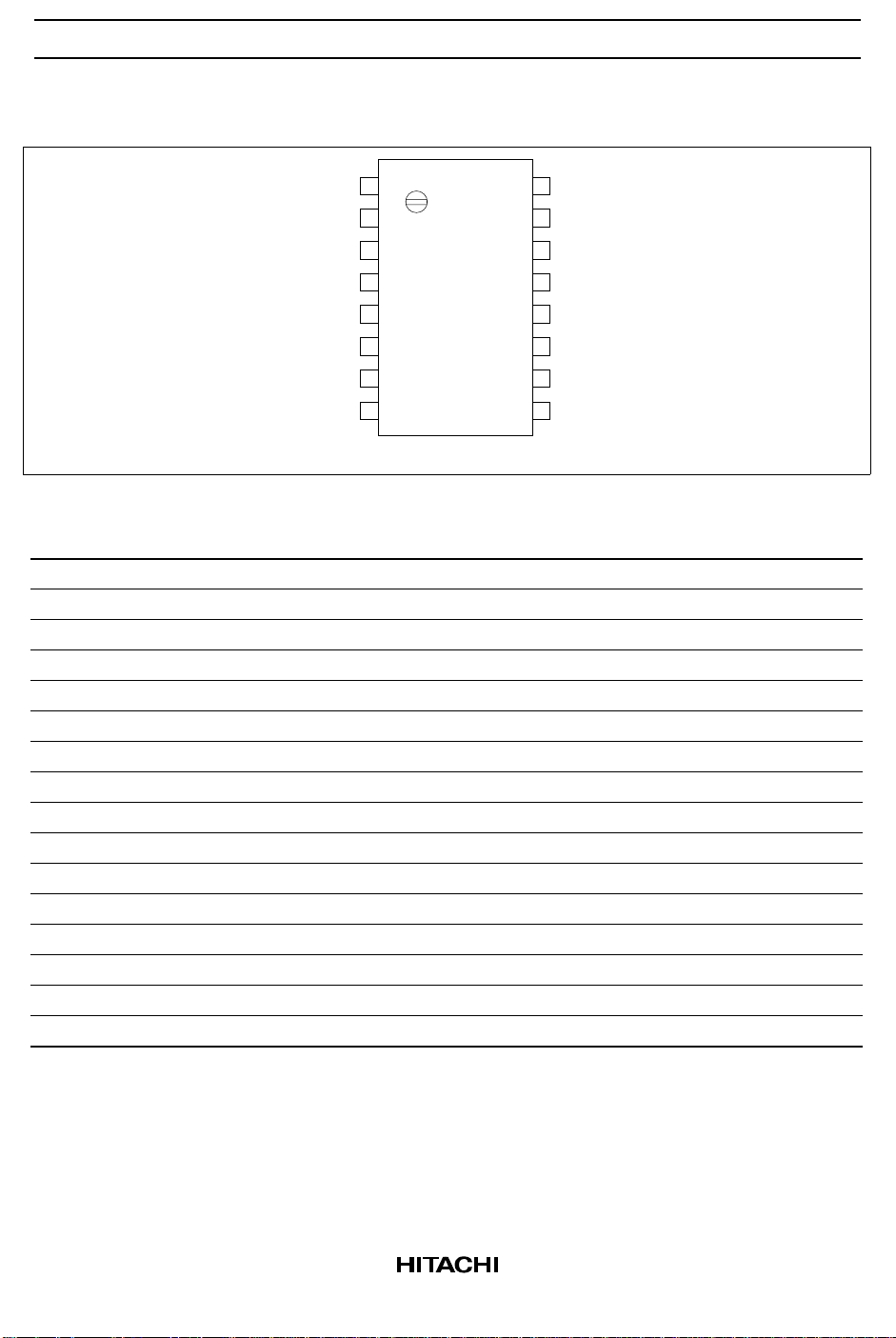
Ordering Information
Type Package
HA16666P DP-16
HA16666FP FP-16DA
2
Page 3
Pin Arrangement
HA16666P/FP
E/I
ST
C
R
T1
R
T2
OSC Out
GND
N.C
1
2
3
T
4
5
6
7
8
16
15
14
13
12
11
10
9
N.INV
–
INV
CS
Vref
V
IN
RM
OUT
N.C
+
(Top View)
Pin Functions
Pin No. Symbol Descreption
1 E/I Error input
2 ST Soft start
3C
T
4RT1Timing resistor (rise section)
5RT2Timing resistor (fall section)
6 OSC Out Triangular waveform oscillator
7 GND Ground
8 N.C No connect
9 N.C No connect
10 OUT Pulse output
11 RM Remote control
12 V
IN
13 Vref Reference voltage (5 V) output
14 CS Comparator input (–) with reference voltage (1.3 V)
15 INV
16 N.INV
–
+
Timing capacitance
Power supply voltage
Comparator input (–) for overcurrent protection
Comparator input (+) for overcurrent protection
3
Page 4
HA16666P/FP
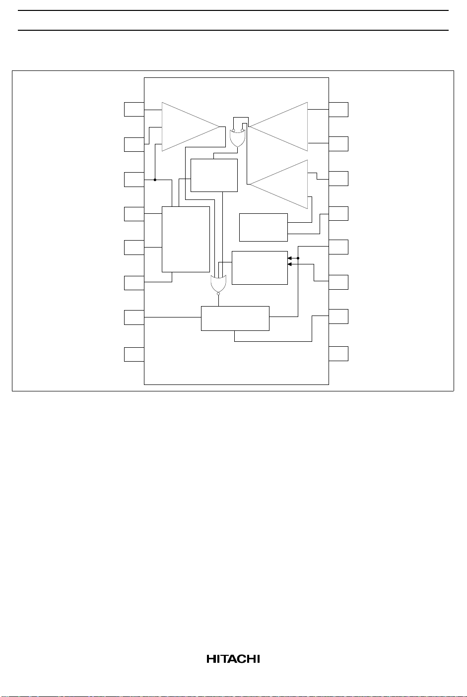
Block Diagram
E/I
ST
C
R
T1
R
T2
OSC Out
GND
N.C
+
1
2
3
T
4
5
6
7
89
PWM
+
comparator
–
R
Triangular
waveform
oscillator
S
S/R
Flip-flop
Output driver
current
detector
Comparator
Reference
voltage
Undervoltage
lockout
protection
Over-
1.3 V
5 V
+
16
–
15
–
14
+
13
12
11
10
N.INV
INV
CS
Vref
V
IN
RM
OUT
N.C
+
–
4
Page 5

HA16666P/FP
Absolute Maximum Ratings (Ta = 25°C)
Rating
Item Symbol HA16666P HA16666FP Unit
Power supply voltage V
Output current DC I
(Push-pull)
Peak I
Error input V
OSC input voltage V
CS input voltage V
RM input voltage V
RT2 input current I
RT1 input current I
Power dissipation P
IN
O(DC)
O(peak)
EI
OSC
CS
RM
R2
R1
T
Operation temperature Topr –20 to +85 –20 to +85 °C
Storage temperature Tstg –55 to +125 –55 to +125 °C
Notes: 1. Value at 300 ns of switiching time
2. Value at Ta ≤ 45°C. If Ta > 45°C, derated by 8.3 mW/°C
3. Value under the condition of 40 mm × 40 mm × 0.8 t ceramics board epoxy board
+40 +40 V
100 100 mA
500*1 500*
1
mA
Vref Vref V
VIN – 3V
BE
VIN – 3V
BE
V
Vref Vref V
V
IN
V
IN
V
11mA
11mA
680*
2
680*
3
mW
Electrical Characteristics (VIN = 15 V, Ta = 25°C, fosc = 300 kHz)
Item Symbol Min Typ Max Unit Test Condition
Voltage Output voltage Vref 4.75 5.00 5.25 V no load
reference
Triangular Maximum frequency f
waveform
oscillator
Line regulation Line — 50 100 mV V
= 11 to 40 V
IN
Load regulation Load — 9 20 mV IO = 0 to 10 mA
Temperature stability V
Short circuit current I
Minimum frequency f
Frequency accuracy f
Voltage stability f
Temperature coefficient
of frequency
RTC
OS
max
min
der
T
f
i
— +60 — ppm/°C no load
10 35 — mA Vref = 0 V
600 — — kHz CT = 150 pF
— — 1 kHz CT = 0.15 µF
–10 0 +10 %
— 1 — % 11 V≤ VIN ≤ 40 V
— 2 — % –20°C ≤ Ta
≤ +85°C
5
Page 6

HA16666P/FP
Electrical Characteristics (VIN = 15 V, Ta = 25°C, fosc = 300 kHz) (cont)
Item Symbol Min Typ Max Unit Test Condition
PWM Maximum duty cycle Du 75 — — %
comparator
Overcurrent Input bias current I
detector
Comparator Input bias current I
Remote
controller
Undervoltage
lockout
protector
Output driver Output low-level V
Total current Standby current I
Note: 1. Measurement conditions of ICS, ICL, tr, tf are defined as following diagram.
Input bias current I
Low-level threshold
B
V
OSCL
–2 — — µA Pin 1
— 1.5 — V Pin 1
voltage
High-level threshold
V
OSCH
— 2.5 — V Pin 1
voltage
Dead-band duty
∆ Du — ±1 ±3%
accuracy
Dead-band duty input
D
T
— 1 — % 11 V≤ VIN ≤ 40 V
voltage stability
Temperature coefficient
D
uT
— 1 — % –20°C ≤ Ta
of dead-band duty
–2 — — µA Pin 15, 16
0 to
V
IN
— — V Pin 15, 16
– 3
—513µAVCS = 5 V
Common-mode input
voltage range
B1
V
CM1
B2
Input threshold voltage Vth 1.2 1.3 1.4 V
Input voltage range V
Input current to remote
CS
I
RM
0 — Vref V
— — 1.5 mA VRM = 5 V
control pin
Input high-voltage V
Input low-voltage V
High-level threshold
INH
INL
V
THH
1——V
— — 0.4 V
91011V
voltage
Low-level threshold
V
THL
789V
voltage
Hysteresis width Hys 1.5 2.0 2.8 V
— 0.7 1.4 V IO
V
IN
——V I
Output high-level V
L
H
– 2.2
Output rise time t
Output fall time t
Operation current I
r
f
CS
CL
— 80 150 ns Note 1
— 40 100 ns Note 1
— 0.15 0.3 mA Note 1
— 8 12 mA Note 1
≤ +85°C
(SINK)
= 10 mA
O
(SOURCE)
= 10 mA
6
Page 7

Waveform Timing
A
9.1
k
330 pF
h
of 2SD667 is defined as 60 min and 200 max.
FE
Ω
Vref V
EI
OSC O/P
R
T2
C
T
R
GND
T1
9.1
Ω
k
V
THH
IN
2SD667
Out
15
2SB647
Ω
2,200 pF
HA16666P/FP
V
THL
V
IN
Remote
control
input
–
INV
+
-N.INV
Overcurrent
detection
signal
E/I
Triangular
waveform
Output
Overcurrent
detection
threshold
Dead-band area
7
Page 8

HA16666P/FP
Characteristic Curves
5.10
Vref Output Voltage vs. Temperature Reference Voltage vs. Input Voltage
5.00
4.90
Reference Output Voltage Vref (V)
4.80
–30 0 50 100
Ambient Temperature T a (°C)
Soft Start Time vs. Soft Start Capacitance
1.0
Ta = 25°C
0.8
0.6
0.4
Soft Start Time (sec)
0.2
Vref
HA16666
ST
51 k
Cs
6.0
Ta = 25
°C
5.0
4.0
3.0
2.0
1.0
Reference Output Voltage Vref (V)
010203040
Input Voltage V (V)
Error Input Voltage/Set Voltage in PWM Comparator
Pulse Duty Cycle vs.
100
90
80
IN
V = 15 V
IN
≅
f 300 kHz
Ta = 25
°C
70
60
50
40
30
Pulse Duty Cycle (%)
20
10
Soft Start Capacitor Capacitance Cs (µF)
100806040200
0.2
0 0.3 0.4 0.5 0.6
Error Input Voltage V
/ ref Voltage
E.I
∆f/f vs. Temperature Dead Band Duty vs. Temperature
+10
C = 330 pF
T
R = R
T2
T1
= 9.1 kΩ
≅
0
f 300 kHz
70
60
C = 330 pF
T
R = R
T2
T1
= 9.1 kΩ
≅
f 300 kHz
f/f (%)
∆
–10
–20020406080
Ambient Temperature T a (°C)
50
Dead-band duty (%)
40
–20 0 20 40 60 80
Ambient Temperature T a (°C)
8
Page 9

VIN Bias Point
10
Back-up supply voltage
HA16666P/FP
C = 330 pF
T
R = R = 9.1 k
T1
V
B
R
B
T2
Ω
15 Ω
+
1 F
2200 pF
5
IN
I (mA)
Quick
shutdown
area
Soft start area
I
IN
12
HA16666
7
D667
10
B647
Under
voltage
lockout
1/R
B
0102083040
V
(V)
IN
9
Page 10

HA16666P/FP
Formula for the oscillation frequency Frequency vs. R
800 k
HA16666
Vref
C
T
C
T
T1
R
Out
T2
R
T1
R
OSC
R
T2
100 k
HA16666 summary formula of the oscillation ferquency
log (f) ≈ a × log (RT1) + b
)
(= R
T2
The following table show empirical values of
a and b for different values of C
C
T
180pF
330pF
1000pF
0.01µF
0.15µF
a
−0.50
−0.61
−0.75
−0.86
−0.86
.
T
b
7.58
7.86
8.09
7.57
6.45
10 k
Frequency f (Hz)
, RT2 Dependence
T1
C
T
120 pF
180 pF
430 pF
1000 pF
3300 pF
0.01 F
µ
10
1 k
51020304050
R = R (k )
T1 T2
Ω
0.033 Fµ
0.15 Fµ
Page 11

System Connection Example
Over current protection; Resistance sensing method
2
R
D
D
10/1 W
2
HA16666P/FP
Output
PHOTO
COUPLER
10
11
R
1 k
R
1 k
9
R
+
7
8
C
R
1 k
6
SHUNT
REGULATOR
K552R330
D667
HA17431P
13
14
R
12
R
B647
C
0.2
1 k
8
C
+
4
3
D
3
C
10
+
Ω
C: F
Unit R:
1,000 p
IN
R
220 k
1
C
+
RFI filter
AC
680
Input
C
2
0.01
876543
N.CGND
RM OUT N.C
IN
CS Vref V
—
15 14 13 12 11 10 9
INV
+
16
N.INV
O/P
OSC
T2
R
T1
R
HA16666P/FP
T
C
2
STE/I
1
6
R
5
R
5
C
3
R
0.047
9.1 k
9.1 k
330 p
50 k
4
C
4
R
10 k
11
Page 12

HA16666P/FP
Over current protection; Current transformer method
Output
PHOTO
COUPLER
10
11
R
1 k
R
1 k
9
R
+
7
8
C
R
1 k
6
SHUNT
REGULATOR
C
+
HA17431P
Ω
C: F
Unit R:
C.T
2
R
2
D
3
D
10/1 W
IN
R
220 k
1
C
680 µ
+
4
D
K552
3
C
10 µ
+
2
C
0.01 µ
R
C
14
R
470
13
3.3 k
8
1,000 p
R
D667
9
C
470 p
6
D
12
11
R
B647
876543
N.CGND
RM OUT N.C
IN
CS Vref V
–
INV
+
16 15 14 13 12 11 10 9
N.INV
O/P
OSC
T2
R
T1
R
HA16666P/FP
T
C
2
STE/I
1
6
R
9.1 k
5
R
9.1 k
5
C
330 p
3
4
R
50 k
R
10 k
4
C
0.047 µ
12
RFI filter
AC
Input
Page 13

Over current protection; Current transformer method
Output
PHOTO
COUPLER
10
11
R
1 k
R
1 k
9
R
+
7
8
C
R
1 k
+
6
C
SHUNT
REGULATOR
HA17431P
HA16666P/FP
Ω
C: F
Unit R:
C.T
2
R
D
3
D
10/1 W
2
IN
R
220 k
1
C
680 µ
+
4
D
K552
3
C
10 µ
+
2
C
0.01 µ
R
C
14
R
470
13
3.3 k
8
1,000 p
R
D667
9
C
470 p
6
D
12
11
R
B647
87654321
N.CGND
RM OUT N.C
IN
CS Vref V
–
INV
+
16 15 14 13 12 11 10 9
N.INV
O/P
OSC
T2
R
T1
R
HA16666P/FP
T
C
STE/I
6
R
9.1 k
5
R
9.1 k
5
C
330 p
3
4
R
50 k
R
10 k
4
C
0.047 µ
RFI filter
AC
Input
13
Page 14

HA16666P/FP
Package Dimensions
19.20
20.00 Max
16 9
1.3
1.11 Max
2.54 ± 0.25
81
0.48 ± 0.10
6.30
7.40 Max
5.06 Max
2.54 Min
0.51 Min
0° – 15°
Hitachi Code
JEDEC
EIAJ
Mass
(reference value)
0.25
7.62
+ 0.13
– 0.05
Unit: mm
DP-16
Conforms
Conforms
1.07 g
10.06
10.5 Max
16
1
0.80 Max
1.27
*0.42 ± 0.08
± 0.06
0.40
*Dimension including the plating thickness
Base material dimension
9
8
0.12
5.5
0.10 ± 0.10
0.15
M
2.20 Max
7.80
0.20 ± 0.04
*0.22 ± 0.05
0.70 ± 0.20
Hitachi Code
JEDEC
EIAJ
(reference value)
Mass
+ 0.20
– 0.30
1.15
0
° – 8°
FP-16DA
—
Conforms
0.24 g
Unit: mm
14
Page 15

HA16666P/FP
Cautions
1. Hitachi neither warrants nor grants licenses of any rights of Hitachi’s or any third party’s patent,
copyright, trademark, or other intellectual property rights for information contained in this document.
Hitachi bears no responsibility for problems that may arise with third party’s rights, including
intellectual property rights, in connection with use of the information contained in this document.
2. Products and product specifications may be subject to change without notice. Confirm that you have
received the latest product standards or specifications before final design, purchase or use.
3. Hitachi makes every attempt to ensure that its products are of high quality and reliability. However,
contact Hitachi’s sales office before using the product in an application that demands especially high
quality and reliability or where its failure or malfunction may directly threaten human life or cause risk
of bodily injury, such as aerospace, aeronautics, nuclear power, combustion control, transportation,
traffic, safety equipment or medical equipment for life support.
4. Design your application so that the product is used within the ranges guaranteed by Hitachi particularly
for maximum rating, operating supply voltage range, heat radiation characteristics, installation
conditions and other characteristics. Hitachi bears no responsibility for failure or damage when used
beyond the guaranteed ranges. Even within the guaranteed ranges, consider normally foreseeable
failure rates or failure modes in semiconductor devices and employ systemic measures such as failsafes, so that the equipment incorporating Hitachi product does not cause bodily injury, fire or other
consequential damage due to operation of the Hitachi product.
5. This product is not designed to be radiation resistant.
6. No one is permitted to reproduce or duplicate, in any form, the whole or part of this document without
written approval from Hitachi.
7. Contact Hitachi’s sales office for any questions regarding this document or Hitachi semiconductor
products.
Hitachi, Ltd.
Semiconductor & Integrated Circuits.
Nippon Bldg., 2-6-2, Ohte-machi, Chiyoda-ku, Tokyo 100-0004, Japan
Tel: Tokyo (03) 3270-2111 Fax: (03) 3270-5109
URL NorthAmerica : http:semiconductor.hitachi.com/
For further information write to:
Hitachi Semiconductor
(America) Inc.
179 East Tasman Drive,
San Jose,CA 95134
Tel: <1> (408) 433-1990
Fax: <1>(408) 433-0223
Europe : http://www.hitachi-eu.com/hel/ecg
Asia (Singapore) : http://www.has.hitachi.com.sg/grp3/sicd/index.htm
Asia (Taiwan) : http://www.hitachi.com.tw/E/Product/SICD_Frame.htm
Asia (HongKong) : http://www.hitachi.com.hk/eng/bo/grp3/index.htm
Japan : http://www.hitachi.co.jp/Sicd/indx.htm
Hitachi Europe GmbH
Electronic components Group
Dornacher Straβe 3
D-85622 Feldkirchen, Munich
Germany
Tel: <49> (89) 9 9180-0
Fax: <49> (89) 9 29 30 00
Hitachi Europe Ltd.
Electronic Components Group.
Whitebrook Park
Lower Cookham Road
Maidenhead
Berkshire SL6 8YA, United Kingdom
Tel: <44> (1628) 585000
Fax: <44> (1628) 778322
Hitachi Asia Pte. Ltd.
16 Collyer Quay #20-00
Hitachi Tower
Singapore 049318
Tel: 535-2100
Fax: 535-1533
Hitachi Asia Ltd.
Taipei Branch Office
3F, Hung Kuo Building. No.167,
Tun-Hwa North Road, Taipei (105)
Tel: <886> (2) 2718-3666
Fax: <886> (2) 2718-8180
Copyright ' Hitachi, Ltd., 1998. All rights reserved. Printed in Japan.
Hitachi Asia (Hong Kong) Ltd.
Group III (Electronic Components)
7/F., North Tower, World Finance Centre,
Harbour City, Canton Road, Tsim Sha Tsui,
Kowloon, Hong Kong
Tel: <852> (2) 735 9218
Fax: <852> (2) 730 0281
Telex: 40815 HITEC HX
15
 Loading...