

Datasheet HA16117FPCJ, HA16117FPC, HA16117FPBJ, HA16117FPB, HA16117FPAJ Datasheet (HIT)
...Page 1

HA16117F Series
CMOS Watchdog Timer
Description
The HA16117F Series of ICs make a micro-processor (MPU) system fail-safe by monitoring its power
supply to detect voltage drops, and monitoring a P-RUN (program running) pulse to detect system crashes.
Also referred to as watchdog timers, these devices are essential in systems that aim for high levels of crash
protection. Fabricated by a CMOS process, they consume little power and are ideally suited for batteryoperated systems.
These ICs are available in versions for industrial and communications equipment and automotive
applications, as well as for consumer products.
Functions
• Power-on reset
Sends a RES signal to the MPU for a fixed time at power-on
• Watchdog timer (WDT)
Monitors a P-RUN signal from the MPU and sends the MPU a RES signal if P-RUN departs from a
set frequency range
• Auto-reset
Outputs RES signals to the MPU at clocked intervals while P-RUN remains abnormal
• Supply voltage supervision
Outputs a low RES signal if the supply voltage (same as the MPU's VCC) falls below a low threshold
level (VTL). The threshold differs for different ICs in the series, allowing designers to choose an IC
matching system requirements (see ordering information)
Features
• Low power consumption : Operating (ACC pin low) = 0.5 mW (Typ)
: Standby (ACC pin high) = 0.2 mW (Typ)
• Watchdog timer on/off control by ACC input signal
• Independent auto-reset high and low times (tRH and tRL)
• Watchdog monitoring by frequency filtering (independent of duty cycle)
• High-precision low voltage detection (±2%)
• Space- and weight-saving 8-pin SOP package
Page 2
HA16117F Series
Ordering Information
The HA16117F Series includes three ICs with different low threshold levels (VTL).
Type No. Low Threshold Voltage (VTL)
HA16117FPA/FPAJ 4.4 V Typ
HA16117FPB/FPBJ 4.2 V Typ
HA16117FPC/FPCJ 4.0 V Typ
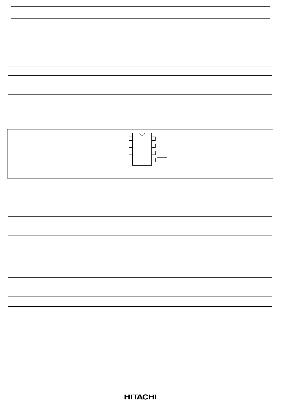
Pin Arrangement
V
CC
P-RUN
C
C
F
R
8
1
7
2
6
3
5
4
(Top view)
Tadj
ACC
GND
RES
Pin Description
Pin No. Symbol Function
1V
CC
2 P-RUN Watchdog timer (WDT) input
3C
4C
F
R
5 RES Reset signal output from WDT and voltage supervision circuits
6 GND Ground
7 ACC WDT on/off control input (on when ACC is low)
8 Tadj * For adjusting tRH and t
Note: The low-voltage threshold cannot be modified by changing the external resistors connected to the
Tadj pin.
Power supply voltage input
Connected capacitor CF determines WDT filter characteristic
(normal frequency range)
Connected capacitor CR determines tON for power-on reset and t
and t
for auto-reset
RL
(divide VCC to get the adjustment voltage)
OFF
OFF
, tRH,
2
Page 3
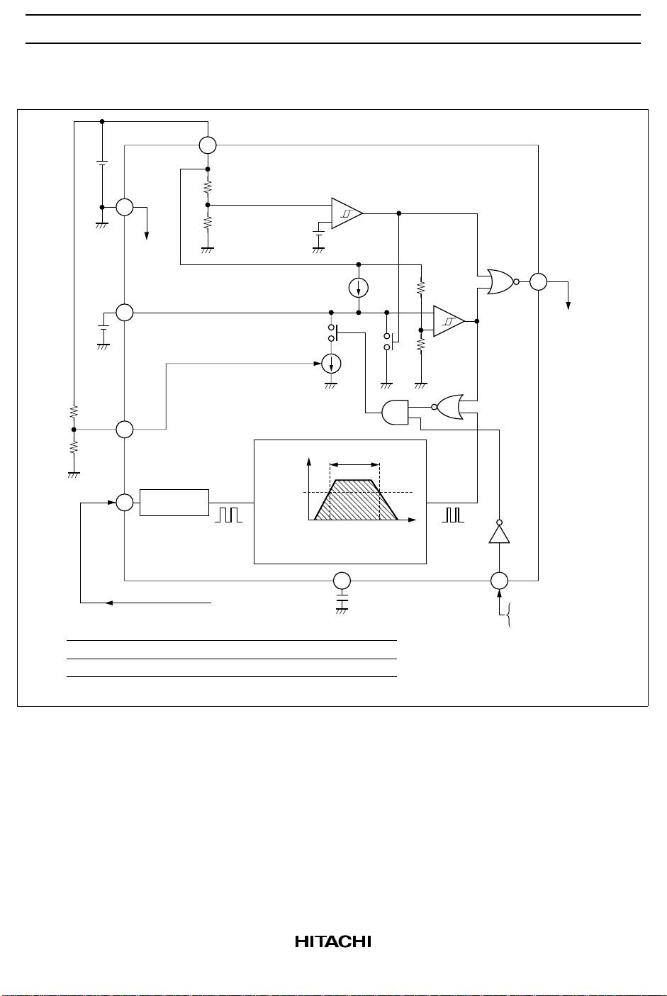
Block Diagram
5 V
6
0.1 µ
4
1
V
CC
2.52 (117FA)
2.36 (117FB)
GND
GND
Power-on and auto-reset circuit
C
R
2.20 (117FC)
1
I2 adjustment
(*I
< I2)
1
Low voltage detector
−
+
≈1.25 V
COMP.
SW2
I
HA16117F Series
RES
I
1
−
+
COMP.
2
SW1
5
to Microcomputer
R
1
510 k
R
2
750 k
Mode
Operating
Standby High
Note: The power-on reset circuit operates in both operating and standby modes.
Tadj
8
P-RUN
1/2 frequency
2
divider
PULSE from I/O port
ACC Voltage Function
Low Low voltage detection and WDT
(SW1 and SW2 are active high)
Watchdog timer
Watchdog filter (f-duty converter)
W.D out
duty (%)
W.D in
duty 50%
Low voltage detection
n
Normal range
f
/2 fH/2
L
W.D in frequency (Hz)
C
F
3 7
0.01 µ
W.D out
duty n%
ACC
Operating: "Low"
Standby: "High"
The HA16117F consists of a low voltage detector, power-on and auto-reset circuit, and watchdog timer.
Low Voltage Detector
Uses a reference voltage source (≈ 1.25 V) and high-precision comparator to detect drops in the supply
voltage.
Power-On and Auto-Reset Circuit
Generates the RES waveform, using a multivibrator consisting of a current source I1 that charges the
external capacitor CR, a current source I2 that discharges CR, and a comparator.
3
Page 4
HA16117F Series
Watchdog Timer
Reshapes the P-RUN signal (programming-running pulse) from the MPU to obtain a 50% duty cycle, then
converts frequency to duty cycle in the watchdog filter (WD filter).
The watchdog filter is a bandpass filter. The duty cycle of the filter output is highest in the normal
frequency range of P-RUN.
The watchdog filter output controls I2 in the multivibrator, the higher the duty cycle of the watchdog filter
output, the shorter the time during which I2 discharges CR. If the duty cycle is high enough then CR is held
at a high potential, preventing the multivibrator from firing, and the RES output remains high.
Absolute Maximum Ratings (Ta = 25°C)
Ratings
Item Symbol HA16117FPA/FPB/FPC HA16117FPAJ/FPBJ/FPCJ Unit
Power supply voltage V
P-RUN input voltage V
ACC input voltage V
RES output current I
Permissible dissipation *
1
CC
P
ACC
RES
P
T
Operating temperature range Topr –30 to +85 –40 to +85 °C
Storage temperature Tstg –55 to +125 –55 to +125 °C
Note: 1. This is the value when mounted on a glass epoxy substrate with 30% wiring density, up to an
ambient temperature of 83°C. Above that temperature, derate by 7.14 mW/°C.
–0.3 to +14 –0.3 to +14 V
V
CC
V
CC
V
14 14 V
10 10 mA
300 300 mW
40mm
(mW)
T
400
60 80
83°C
85°C
100
300
200
100
0
−30 −20 0 20 40
Ambient operating temperature range Ta (°C)
Permissible dissipation P
−7.14 mW/°C
(30% wiring density)
Substrate
0.8 mm ceramic or
1.5 mm epoxy
4
Page 5
HA16117F Series
Electrical Characteristics
(VCC = 5 V, Ta = 25°C, CF = 0.01 µF, CR = 0.1 µF, R1 = 510 kΩ, R2 = 750 kΩ)
Item Symbol Min Typ Max Unit Test Conditions
General Operating supply current I
Standby supply current I
Low
voltage
detector
Low voltage
threshold
level
HA16117FPA/FPAJ V
HA16117FPB/FPBJ 4.1 4.2 4.3 V
HA16117FPC/FPCJ 3.9 4.0 4.1 V
Hysteresis width V
ACC Low input voltage V
High input voltage V
P-RUN Low input voltage V
input High input voltage V
WDT Power-on reset time t
Reset-clock off time t
Reset low time t
Reset high time t
Low setup time t
High setup time t
RES RES low voltage V
output RES high voltage V
Reset function starting voltage V
Constant
Constant range of R1 and R
2
range
Operating supply voltage range V
Note: 1. Reset-clock off time t
is provided a shown in the under figure.
OFF
CC1
I
CC2
STBY
TL
HYS
IL1
IH1
IL2
IH2
ON
OFF
RL
RH
SL
SH
OL
OH
RES
K 0.55 0.6 0.8 — K =R2 / (R1 + R2)
CCRNG
— 100 — µAV
— 200 600 µAV
— 43 100 µAV
4.3 4.4 4.5 V
50 100 150 mV
— — 0.8 V
2.0 — — V
— — 0.8 V
2.0 — — V
24 40 56 ms
1
*
78 130 182 ms
12 20 28 ms
36 60 84 ms P-RUN pin = 0 V
1——ms
——1 ms
— — 0.4 V IOL = 1 mA
—VCC— V Open
— 0.8 1.4 V
V
TL
— 6.0 V
= 0 V,
ACC
f
= 100 Hz
P-RUN
= 0 V,
ACC
f
= 20 kHz
P-RUN
= 12 V
ACC
When VCC drops
P-RUN
RES
f = 500 Hz, Duty = 50%
t
OFF
5
Page 6
HA16117F Series
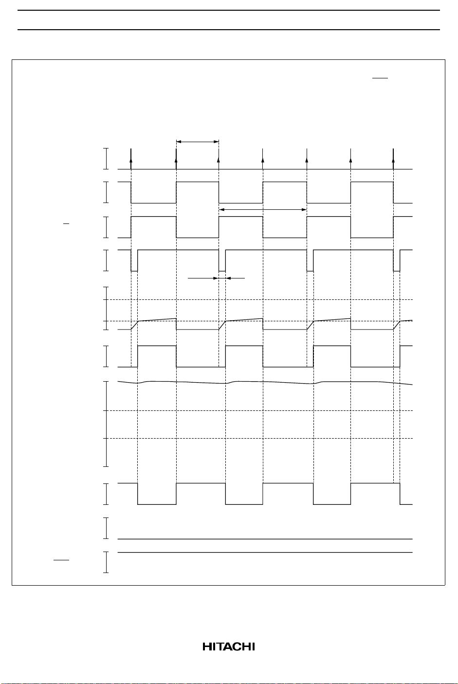
Timing Waveforms and Functional Description
V
CC
V
TL
P-RUN
Watchdog function on
RES
(V
= "Low")
ACC
Watchdog function off
RES
(V
= "High")
ACC
t
ON
t
ON
Crash
t
RH
t
OFF
t
RL
t
ON
t
ON
Figure 1 Timing Waveforms
Watchdog On/Off Function
A feature of the HA16117F is that watchdog supervision can be switched on and off. When the watchdog
function is switched on, both the supply voltage and
P-RUN input are monitored to detect abnormal conditions. When the watchdog function is switched off
(standby mode), only the supply voltage is monitored. Watchdog supervision is switched on and off by the
input at the ACC pin (pin 7): Supervision is on when ACC is low, and off when ACC is high.
Many MPUs have a standby mode in which the CPU stops running but memory contents are retained. In
standby mode, program execution halts and I/O ports go to the high-impedance state, so there is no need for
the watchdog timer to supervise pulse output from an I/O port to detect abnormal conditions. Power can be
saved by placing both the MPU and HA16117F in standby mode at the same time. The HA16117F is
designed to draw a typical standby current I
of only 43 µA Typ when the watchdog function is switched
STBY
off.
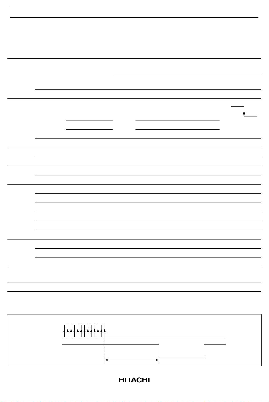
ACC Pin (pin 7) and RES Output
When the MPU returns from standby mode to normal operation it generally takes 10 to 200 ms for the
clock oscillator in the MPU to stabilize. The RES signal is not output during this setup time. After the
setup time (tSL) has elapsed, RES is output if the P-RUN signal from the MPU is still abnormal.
ACC pin
RES (due to MPU crash)
t
SH
Adjust according to
MPU’s setup time
t
SL
Figure 2 ACC Pin and RES Output
6
Page 7
HA16117F Series
Internal Operation and Usage Notes
Figure 3 shows an equivalent circuit of the watchdog timer block with a VCC pin level of 5 V and ACC pin
level of 0 V, and the following pages show internal operation timing charts for different P-RUN
frequencies. (Descriptions apply to conditions CF = 0.01 µF, CR = 0.1 µF, R2/(R1 + R2) = 0.6.)
Operation
The power-on and auto-reset circuit is a multivibrator with timing controlled by CR charge current I1 and
discharge current I2. As I1 : I2 ≈ 3 : 1 (Typ design value), when the (WD) (watchdog filter circuit output)
on-duty is 25% or above, the CR pin potential does not fall below 1.6 V. Therefore, (C) in the figure below
is fixed low, and RES is not output. The (WD) on-duty varies according to the P-RUN frequency. If the
frequency is lower or higher than the design value, the (WD) on-duty decreases, and at 25% or below, RES
is output. Refer to the timing charts on the following pages for an explanation of the operation of the
watchdog filter.
Usage Notes
• When the P-RUN frequency reaches 20 kHz or above, t
is short (see the timing charts on the
OFF
following pages). This must be borne in mind in the design stage.
• If the P-RUN frequency fluctuates, RES may also be output within the normal detection set frequency
(see the timing charts on the following pages).
• Detection frequencies fH and fL described in the Data Book are Typ values, and a certain amount of
dispersion can be expected. A margin of ±30% or more should be allowed for in the design.
0.1 µ
B
C
R
I
1
8 µ typ
3.2 V
1.6 V
I
2
10.7 µ
typ
Power-on and auto-reset circuitWatchdog filter circuit
Low voltage detection block
C
−
+
RES
I
w
0.8 µ
typ
C
F
0.01 µ
P-RUN
A
3.6 V
Q
QD
φ
Q
1/2
frequency divider
0.9 V
Q
VCC (5 V)
−
+
−
+
WD
Figure 3 Watchdog Timer Evaliation Circuit
7
Page 8
HA16117F Series
1. When P-RUN signal is not input
P-RUN
C
WD
The watchdog filter circuit output (WD) is fixed low, so the RES signal is output as shown in
the figure below in accordance with power-on and auto-reset circuit C
H
L
H
Q
L
H
Q
L
H
A
L
5 V
3.6 V
F
0.9 V
0 V
H
L
5 V
charge/discharge.
R
3.2 V
C
R
1.6 V
0 V
H
B
L
H
C
L
H
RES
L
20 ms
60 ms
8
Page 9
2. With a low-frequency P-RUN signal ( 13 Hz to 26 Hz)
HA16117F Series
P-RUN
C
WD
When f
duty is 25% or above, multivibrator (power-on and auto-reset circuit) oscillation stops. As a
is 13 Hz to 26 Hz, the WD duty (D = 100 × t2/2T) is 25% to 50%. When the WD
P-RUN
result, the RES signal is fixed high.
40 ms (25 Hz)
H
L
H
Q
L
H
2T
Q
L
H
A
L
5 V
3.6 V
F
0.9 V
0 V
5 µs
t
1
H
t
L
2
33 ms
5 V
C
RES
3.2 V
R
1.6 V
0 V
H
B
L
H
C
L
H
60 ms
L
20 ms
9
Page 10
HA16117F Series
3. With a 10 kHz P-RUN signal
P-RUN
C
WD
When f
25%, the multivibrator (power-on and auto-reset circuit) does not oscillate. The RES signal
remains high.
H
L
H
Q
L
H
Q
L
H
A
L
5 V
3.6 V
F
0.9 V
0 V
H
L
5 V
is 10 kHz, the WD duty (D = 100 × (T − t2)/2T) is 48%. As the duty is above
P-RUN
100 µs (10 kHz)
2T
t
µs
1 5
10
C
RES
3.2 V
R
1.6 V
0 V
H
B
L
H
C
L
H
L
Page 11

4. With a 150 kHz P-RUN signal
HA16117F Series
P-RUN
C
WD
When f
Therefore, C
is 100 kHz or above, the WD duty (D = 100 × (T − t2)/2T) is 25% or below.
P-RUN
is discharged, and the RES signal is output at the instant that the pin potential
R
falls to the comparator circuit threshold value (V
6.6 µs (150 kHz)
H
L
H
Q
L
H
2T
Q
L
H
A
L
5 V
3.6 V
F
t
5 µs
1
0.9 V
0 V
H
L
5 V
= 1.6 V).
TL
C
RES
3.2 V
R
1.6 V
0 V
H
B
L
H
C
L
H
L
11
Page 12

HA16117F Series
5. t
when P-RUN signal 90 kHz
OFF
P-RUN
C
WD
When the P-RUN frequency is high, even though within specification, the C
falls. If the P-RUN frequency falls sharply at this time, t
may be short.
OFF
pin potential
R
With values of CF = 0.01 µF and CR = 0.1 µF, the CR pin potential will not fall as long as the
P-RUN frequency is 20 kHz or below.
≈ 90 kHz
f
H
P_RUN
50 ms
L
H
Q
L
H
Q
L
H
A
L
5 V
3.6 V
F
0.9 V
0 V
H
L
5 V
12
C
RES
3.2 V
R
≈ 2.3 V
1.6 V
0 V
H
B
L
H
C
L
H
L
t
OFF
26 ms
Page 13

6. When P-RUN frequency fluctuates (1)
If there is a double-pulse in P-RUN, the WD filter duty will be decreased and RES will be
output, as shown in the figure below, for example. In this case, the condition for non-output of
the RES signal is a value of 3 or less for the ratio of P-RUN pulse interval minimum value to
P-RUN
C
WD
maximum value (when f
ratio is 3.
H
L
H
Q
L
H
Q
L
H
A
L
5 V
3.6 V
F
0.9 V
0 V
H
L
5 V
P-RUN
2 ms
28 ms
HA16117F Series
≤ 20 kHz). This is because the CR pin charge/discharge current
C
RES
3.2 V
R
1.6 V
0 V
H
B
L
H
C
L
H
L
20 ms
13
Page 14

HA16117F Series
7. When P-RUN frequency fluctuates (2)
If there is a double-pulse in P-RUN, RES will not be output as long as the ratio of P-RUN
pulse interval minimum value to maximum value is 3 or less. The timing chart for a P-RUN
minimum interval of 8 ms and maximum interval of 22 ms is shown below.
P-RUN
C
WD
C
H
L
H
Q
L
H
Q
L
H
A
L
5 V
3.6 V
F
0.9 V
0 V
H
L
5 V
3.2 V
R
1.6 V
8 ms
22 ms
14
0 V
H
B
L
H
C
L
H
RES
L
Page 15

8. Summary of cases where P-RUN frequency fluctuates
If there is a double-pulse in P-RUN, RES may be output if the double-pulse has multiple frequency
components. If the P-RUN frequency fluctuates, refer to the following when making the P-RUN
setting.
• P-RUN normal detection region, duty dependency
1 M
100 k
(Hz)
10 k
P-RUN
HA16117F Series
Note: 1
When f
t
is frequency-dependent,
OFF
so care is required when
making the P-RUN setting
(see figure below).
P-RUN
≥ 20 kHz,
1 k
100
P-RUN frequency f
10
1
050
Note: 2. This is the region when f
If f
fluctuates within the normal detection region, the following applies:
P-RUN
Normal detection is performed when the condition f
• f
dependency of VCR, t
P-RUN
5
4
(V)
CR
3
Normal detection region*
P-RUN pulse duty D (%)
is constant.
P-RUN
, M
OFF
2
100
P-RUN H/fP-RUN L
< M is satisfied.
t
(s)
OFF
3
100 m
M
2
50 m
2
Multivibrator threshold voltage (1.6 V)
1
CR voltage V
0
1 k 3 k 10 k
P-RUN frequency (Hz)
0
1
30 k 50 k 70 k 100 k7 k5 k
15
Page 16

HA16117F Series
Setting of RES Timing and Watchdog Frequency Range
Different MPUs have different RES timing requirements. The minimum reset time (tON) required at poweron (rise of VCC) is 20 ms for some MPUs and 100 ms for others.
RES timing waveform parameters must be selected according to the MPU. With the HA16117F the timing
of the RES output and the watchdog frequency range can both be set by external constants (CF, CR, and K).
Parameters
Item Symbol CR (pin 4) CF (pin 3) K (pin 8) *
Power-on reset time t
Reset-clock off time t
Reset low time t
Reset high time t
Watchdog frequency high f
Watchdog frequency low f
ON
OFF
RL
RH
H
L
●
●▲ *
2
●
●
●●
●●
●●●
Notes: 1. K = R2 / (R1 + R2)
2. Variability of t
3.3 (MΩ) × C
increases with increasing CF. The variability ∆t
OFF
(µF), so CF ≤ 0.01 (µF) is recommended.
F
is approximately
OFF
3. External constants should be selected with reference to the formulas in tables 1 and 2.
1
Table 1 Calculation of RES Output Timing
Item Formula Notes
(ms) 400 (Ω) × CR (µF) tON and t
t
ON
t
(ms) 1.99 × tRH (ms)
OFF
can be set independently
OFF
tRL (ms) 0.5 × tON (ms) tRL and tRH can be set independently
tRH (ms)
K × 31 (µA) − 15.8 (µA)
tSL (ms) ≈ t
OFF
(ms)
1.6 (V)
× C
(µF) × 10
R
3
Table 2 Calculation of Watchdog Frequency Range
Item Formula
(MHz)
f
H
fL (Hz)
500 (Ω) × C
1.7 (MΩ) × C
Whichever is larger
1
(µF)
F
1
(µF)
F
(ms) − tRL (ms)
t
RH
×
t
(ms) + tRL (ms)
RH
(ms)
t
×× 10
RL
t
(ms) + tRL (ms)
RH
or
1
t
(ms)
OFF
3
16
Page 17

HA16117F Series
Selection of External Constants
If the reset duration necessary for the MPU to operate reliably at power-on is known, there is a simple
procedure for selecting external constants, starting from the power-on reset time (tON).
External
START
Set power-on
reset time t
ON
Set reset high
time t
RH
Select external
constant C
F
Check watchdog
frequency range
fH and f
L
constant
values
• Decide reset
low time (tRL)
• Select external
constant C
R
Application Example
Battery
5 V
regulator
0.01 µF
• Decide reset-clock
off time (t
OFF
)
• Select external
constants R1 and R
2
Figure 4 Procedure for Selecting External Constants
SW
R
1
510 kΩ
C
F
0.1 µF
V
CC
P-RUN
HA16117F
C
F
C
C
R
R
Tadj
ACC
GND
RES
R
2
750 kΩ
V
CC
Microprocessor
system
PORT GND
RES
17
Page 18

HA16117F Series
Operating Characteristics and Test Circuits
V
CC
RES
P-RUN
RES
5 V
V
0 V
5 V
0 V
5 V
0 V
5 V
0 V
510 k
TL
t
ON
5V
0V
0.01 µ 0.1 µ
V
CC
Tadj
P-RUN ACC
C
C
GND
F
RES
R
750 k
Oscilloscope
50 ms/div time
Circuit for measuring t
ON
Power-on reset time (tON)
SW,OFF
t
OFF
5V
0V
f = 500Hz
duty 50%
0.01 µ 0.1 µ
50‰
5 V
V
CC
Tadj
P-RUN ACC
C
C
GND
F
RES
R
510 k
750 k
Oscilloscope
50 ms/div time
Reset-clock off time (t
OFF
)
Circuit for measuring t
OFF
18
5 V
0 V
RES and C
t
RH
RES
C
R
t
RL
20 ms/div time
waveforms at detect abnormal conditions
R
5V
V
P-RUN ACC
C
C
CC
F
R
Tadj
GND
RES
0.01 µ 0.1 µ
Oscilloscope
Oscilloscope
Circuit for measuring RES and CR waveforms
510 k
750 k
Page 19

Low Voltage Threshold vs. Ambient Temperature
5.0
HA16117FA
V -Ta
TL
(V)
TL
4.5
(−50ppm/°C)
4.0
Low voltage threshold V
3.5
−30 0 50 85
Ambient temperature Ta (°C)
V
CC
0.01 µ 0.1 µ
CC
Tadj
V
P-RUN ACC
C
C
GND
F
RES
R
Test circuit
HA16117F Series
12 V
510 k
750 k
5 V
regulator
Oscilloscope
Threshold Hysteresis Width vs. Ambient Temperature
150
HA16117FA
V -Ta
HYS
(mV)
HYS
100
V
50
Threshold hysteresis width V
0
−30 0 50 85
Ambient temperature Ta (°C)
V
CC
P-RUN ACC
C
C
0.01 0.1
CC
F
R
Test circuit
Tadj
GND
RES
Oscilloscope
12V
510k
750k
5 V
regulator
19
Page 20

HA16117F Series
500 µ
Ta = 25°C
(A)
CC
100 µ
Operating supply current I
10 µ
100 1 k 10 k 20 k
Operating Supply Current vs. P-RUN Input Frequency
P-RUN input frequency f
P-RUN
(Hz)
20
Pulse genelator
VCC pin
5 V
0 V to 5 V
0.01 µ 0.1 µ
A
I
CC
V
CC
P-RUN ACC
C
F
C
R
Test circuit
Tadj
GND
RES
510 k
750 k
Page 21

Standby Supply Current vs. Supply Voltage
200 µ
HA16117F Series
Ta = 25°C
(A)
STBY
100 µ
Standby supply current I
0
Supply Voltage VCC (V)
0.01 µ 0.1 µ
57
Supply Current vs. Ambient Temperature
300 µ
A
I
STBY
V
CC
P-RUN ACC
C
F
C
R
Test circuit
Tadj
GND
RES
510 k
750 k
V
12 V
V
CC
(A)
CC
, I
STBY
200 µ
f = 20 kHz I
f = 100 Hz I
100 µ
Supply current I
I
STBY
0
−30 0 50 85
Ambient temperature Ta (°C)
CC
CC
21
Page 22

HA16117F Series
RES Low Voltage vs. RES pin Sink Current
0.4
0.3
(V)
OL
5 V
CC
Tadj
V
P-RUN ACC
51 k
75 k
0.2
≈ 160Ω)
ON
(R
0.1
RES low voltage V
0 0.5 m 1 m 1.5 m
RES pin sink current I
OL
(V)
OL
RES low voltage V
C
F
C
R
0.01 µ
Test circuit
(A)
RES Low Voltage vs. Ambient Temperature
0.3
IOL = 1mA
0.2
0.1
GND
RES
V
I
o sink
22
0
−30 0 50 85
Ambient temperature Ta (°C)
Page 23

RES High Voltage vs. RES pin Source Current
5
Ta = 25°C
(V)
OH
5V
HA16117F Series
CC
Tadj
V
P-RUN ACC
51 k
75 k
4
RES high voltage V
3
0
RES pin source current I
o source
(A)
500 µ
0.01 µ 0.1 µ
C
F
C
R
Test circuit
GND
RES
V
I
o sink
23
Page 24

HA16117F Series
Power-on Reset Time vs. C
R
1
Ta = 25°C
100 m
(sec)
ON
10 m
Power-on reset time t
1 m
0.01 µ 0.1 µ 1.0 µ
External capacitance C
RES Output Timing vs. C
R
1
Ta = 25°C
Capacitance
(F)
R
Capacitance
5V
0.01 µ C
V
CC
P-RUN ACC
C
F
C
R
R
V
CC
RES
Test circuit
GND
RES
t
ON
Tadj
510 k
750 k
Oscilloscope
(sec)
100 m
RL
, t
RH
t
RH
t
RL
10 m
RES output timing t
1 m
0.01 µ 0.1 µ 1.0 µ
External capacitance C
R
(F)
5 V
0.01 µ C
V
CC
P-RUN ACC
C
F
C
R
R
Test circuit
RES
Tadj
GND
RES
5 V
0 V
510 k
750 k
Oscilloscope
t
RH
24
Page 25

HA16117F Series
High Setup Time vs. C
1000 µ
Ta = 25°C
100 µ
(sec)
SH
10 µ
High setup time t
1 µ
0.01 µ
External Capacitance CR (F)
Capacitance
R
0.1 µ 1.0 µ
0.01 µ
5 V
C
R
V
CC
Tadj
P-RUN ACC
C
C
GND
F
RES
R
Test circuit
510 k
750 k
RES
Oscilloscope
0V
t
SH
Low Setup Time vs. C
Capacitance
R
10
Ta = 25°C
1
(sec)
SL
100 m
Low setup time t
10 m
0.01 µ 0.1 µ 1.0 µ
External Capacitance CR (F)
5 V
0.01 µ C
V
CC
P-RUN ACC
C
F
C
R
R
Test circuit
Tadj
GND
RES
Oscilloscope
15 V
0 V
RES
510 k
750 k
t
SL
25
Page 26

HA16117F Series
Reset High Time vs. K (Tadj Constant)
100 m
(sec)
RH
5 V
CC
Tadj
V
P-RUN ACC
R
1
R
2
Reset high time t
10 m
0.56 0.6 0.7 0.8
Tadj constant K
Duty-cycle dependence of
P-RUN normal frequency range
1 M
MPU system abnormal
100 k
Abnormal if duty
cycle is 0%
10 k
(Hz)
P-RUN
MPU system normal
1 k
Abnormal if duty
100
cycle is 100%
0.01 µ 0.1 µ
Pulse
generator
5 V
0 V
0.01 µ 0.1 µ
5 V
C
C
GND
F
RES
R
Test circuit
V
CC
Tadj
P-RUN ACC
C
C
GND
F
RES
R
Oscilloscope
K =
510 R
750 R
Oscilloscope
R
2
R
+ R
1
2
26
10
P-RUN input frequency f
MPU system abnormal
1
0
50 100
P-RUN input pulse duty cycle (%)
Test circuit
Notes: 1.2.Normal detection is assumed when RES is not output.
The figure at left is for a constant P-RUN frequency.
See "8. Summary of cases where P-RUN frequency
fluctuates" for cases where the frequency fluctuates.
Page 27

P-RUN Input Frequency vs. K (Tadj constant)
1 M
Ta = 25°C
K=
R1 + R
R
2
2
100 k
(Hz)
10 k
P-RUN
1 k
MPU system normal
100
P-RUN input frequency f
10
Pulse
generator
5V
0V
duty 50%
0.01 µ
5 V
0.1 µ
Test circuit
HA16117F Series
R
V
P-RUN ACC
C
C
CC
F
R
Tadj
GND
RES
Oscilloscope
K =
R
1
R
2
R
2
+ R
1
2
MPU system abnormal
1
0.55
0.6
0.7 0.8
Tadj constant K
P-RUN High Threshold Frequency vs. C
10 M
Ta = 25°C
(Hz)
H
MPU system abnormal
1 M
100 k
P-RUN high threshold frequency f
MPU system normal
10 k
500 p
1000 p 0.01 µ 0.03 µ
External capacitance CF (F)
Notes: 1.2.Normal detection is assumed when RES is not output.
Capacitance
F
Notes: 1.2.Normal detection is assumed when RES is not output.
The figure at left is for a constant P-RUN frequency.
CC
F
R
Tadj
GND
RES
5 V
Pulse
V
P-RUN ACC
C
C
generator
C
F
C
R
Oscilloscope
0 V to 5 V duty 50%
Test circuit
The figure at left is for a constant P-RUN frequency.
510 k
750 k
27
Page 28

HA16117F Series
P-RUN Low Threshold Frequency vs. CF Capacitance
1 k
Ta = 25°C
(Hz)
L
100
Normal
CR = 0.01 µF
CR = 0.1 µF
5 V
Pulse
generator
V
CC
Tadj
P-RUN ACC
C
C
GND
F
RES
R
51 k
75 k
Abnormal
10
P-RUN low threshold frequency f
CR = 1.0 µF
500 p11000 p 0.01 µ 0.03 µ
External Capacitance CF (F)
P-RUN Input Frequency vs. Ambient Temperature
1 M
P-RUN abnormal
100 k
(Hz)
10 k
P-RUN
1 k
f
H
P-RUN normal
C
F
C
R
Oscilloscope
Test circuit
Notes: 1.2.Normal detection is assumed when RES is not output.
The figure at left is for a constant P-RUN frequency.
510 k
750 k
5 V
duty 50%
V
CC
Tadj
P-RUN ACC
C
C
GND
F
RES
R
Pulse
generator
Oscilloscope
28
100
f
L
P-RUN input frequency f
10
P-RUN abnormal
1
−30
0
Ambient temperature Ta (°C)
50 85
0.01 µ
0.1 µ
Test circuit
Notes: 1.2.Normal detection is assumed when RES is not output.
The figure at left is for a constant P-RUN frequency.
Page 29

HA16117F Series
Power-on Reset Time vs. Ambient Temperature
100
(ms)
ON
50
t
ON
Power-on reset time t
−3000 50 100
Ambient temperature Ta (°C)
Power-on Reset Time vs. Ambient Temperature
and tRL vs. Ambient Temperature
t
RH
100
70
t
RH
50
(ms)
RL
5 V
0.01 µ C
R
RES
5 V
0.01 µ 0.1 µ
V
CC
P-RUN ACC
C
F
C
R
V
CC
Test circuit
V
CC
P-RUN ACC
C
F
C
R
GND
RES
t
ON
GND
RES
Tadj
Tadj
510 k
750 k
Oscilloscope
51 k
75 k
and t
RH
t
30
t
RL
0
−35 0 50 85
Ambient temperature Ta (°C)
5 V
0 V
Test circuit
Oscilloscope
t
RH
t
RL
29
Page 30

HA16117F Series
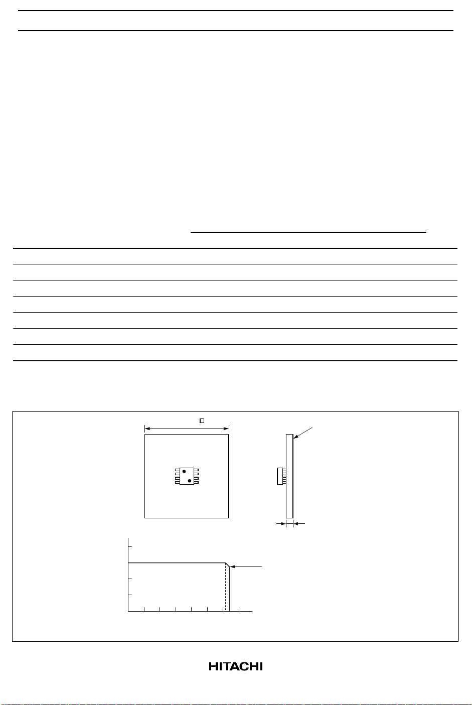
Package Dimensions
1.27
4.85
5.25 Max
8
1
0.75 Max
Unit: mm
5
4.4
4
+ 0.25
6.50
– 0.15
2.03 Max
*0.22 ± 0.05
1.05
0.20 ± 0.04
0° – 8°
+ 0.25
0.60
– 0.18
*0.42 ± 0.08
0.40 ± 0.06
*Dimension including the plating thickness
Base material dimension
0.10 ± 0.10
0.12
0.15
M
Hitachi Code
JEDEC
EIAJ
Mass
(reference value)
FP-8D
—
Conforms
0.10 g
30
Page 31

HA16117F Series
Cautions
1. Hitachi neither warrants nor grants licenses of any rights of Hitachi’s or any third party’s patent,
copyright, trademark, or other intellectual property rights for information contained in this document.
Hitachi bears no responsibility for problems that may arise with third party’s rights, including
intellectual property rights, in connection with use of the information contained in this document.
2. Products and product specifications may be subject to change without notice. Confirm that you have
received the latest product standards or specifications before final design, purchase or use.
3. Hitachi makes every attempt to ensure that its products are of high quality and reliability. However,
contact Hitachi’s sales office before using the product in an application that demands especially high
quality and reliability or where its failure or malfunction may directly threaten human life or cause risk
of bodily injury, such as aerospace, aeronautics, nuclear power, combustion control, transportation,
traffic, safety equipment or medical equipment for life support.
4. Design your application so that the product is used within the ranges guaranteed by Hitachi particularly
for maximum rating, operating supply voltage range, heat radiation characteristics, installation
conditions and other characteristics. Hitachi bears no responsibility for failure or damage when used
beyond the guaranteed ranges. Even within the guaranteed ranges, consider normally foreseeable
failure rates or failure modes in semiconductor devices and employ systemic measures such as failsafes, so that the equipment incorporating Hitachi product does not cause bodily injury, fire or other
consequential damage due to operation of the Hitachi product.
5. This product is not designed to be radiation resistant.
6. No one is permitted to reproduce or duplicate, in any form, the whole or part of this document without
written approval from Hitachi.
7. Contact Hitachi’s sales office for any questions regarding this document or Hitachi semiconductor
products.
Hitachi, Ltd.
Semiconductor & Integrated Circuits.
Nippon Bldg., 2-6-2, Ohte-machi, Chiyoda-ku, Tokyo 100-0004, Japan
Tel: Tokyo (03) 3270-2111 Fax: (03) 3270-5109
URL NorthAmerica : http:semiconductor.hitachi.com/
For further information write to:
Hitachi Semiconductor
(America) Inc.
179 East Tasman Drive,
San Jose,CA 95134
Tel: <1> (408) 433-1990
Fax: <1>(408) 433-0223
Europe : http://www.hitachi-eu.com/hel/ecg
Asia (Singapore) : http://www.has.hitachi.com.sg/grp3/sicd/index.htm
Asia (Taiwan) : http://www.hitachi.com.tw/E/Product/SICD_Frame.htm
Asia (HongKong) : http://www.hitachi.com.hk/eng/bo/grp3/index.htm
Japan : http://www.hitachi.co.jp/Sicd/indx.htm
Hitachi Europe GmbH
Electronic components Group
Dornacher Straβe 3
D-85622 Feldkirchen, Munich
Germany
Tel: <49> (89) 9 9180-0
Fax: <49> (89) 9 29 30 00
Hitachi Europe Ltd.
Electronic Components Group.
Whitebrook Park
Lower Cookham Road
Maidenhead
Berkshire SL6 8YA, United Kingdom
Tel: <44> (1628) 585000
Fax: <44> (1628) 778322
Hitachi Asia Pte. Ltd.
16 Collyer Quay #20-00
Hitachi Tower
Singapore 049318
Tel: 535-2100
Fax: 535-1533
Hitachi Asia Ltd.
Taipei Branch Office
3F, Hung Kuo Building. No.167,
Tun-Hwa North Road, Taipei (105)
Tel: <886> (2) 2718-3666
Fax: <886> (2) 2718-8180
Copyright ' Hitachi, Ltd., 1998. All rights reserved. Printed in Japan.
Hitachi Asia (Hong Kong) Ltd.
Group III (Electronic Components)
7/F., North Tower, World Finance Centre,
Harbour City, Canton Road, Tsim Sha Tsui,
Kowloon, Hong Kong
Tel: <852> (2) 735 9218
Fax: <852> (2) 730 0281
Telex: 40815 HITEC HX
31
 Loading...